

MELEXIS TH8055JDC Datasheet

TH8055
Single Wire CAN Transceiver
Features and Benefits
Fully compatible with J2411 Single Wir e CAN specification for Class B in vehicle
communications
30 µA typical power consumption in sleep mode independent from CAN voltage range
Operating voltage range 5…18V
Up to 100 kbps high-speed transmission mode
Up to 40 kbps bus speed
Selective BUS wakeup
Low RFI due to output wave shaping
Fully integrated receiver filter
Bus terminals proof against shor t-circuits and transients in automotive environment
Loss of ground protection
Protection against load dump, jum p st ar t
Thermal overload and short circuit prot ect ion
ESD protection of 4 kV on CAN pin (2kV on any other pin)
Under- and over voltage lock out
Bus dominant timeout feature
Ordering Information
Part No. Temperature Suffix Package
TH8055 J (-40 ….125 °C) DC (SOIC 150mil)
General Description
The TH8055 is a physical layer device for a single wire
data link capable of operating with various CSMA/CR
protocols such as the Bosch Controller Area Network
(CAN) version 2.0. This serial data link network is
intended for use in applications where high data rate is
not required and a lower data rate can achieve cost
reductions in both the physical media components and
in the microprocessor and/or dedicated logic devices
which use the network.
The network shall be able to operate in either the
normal data rate mode or a high speed data download
mode for assembly line and service data transfer
operations. The high speed mode is only intended to be
operational when the bus is attached to an off-board service
node. This node shall provide temporary bus electrical loads
which facilitate higher speed operation. Such temporary
loads shall be removed when not performing download
operations.
The bit rate for normal communications is typically 33 kbit/s,
for high speed transmissions like described above a typical
bit rate of 83 kbit/s is recommended. The TH8055 is
designed in accordance to the Single Wire CAN Physical
Layer Specification GMW3089 V1.4 and supports many
additional features like undervoltage lockout , timeout for
faulty blocked input signals, output blanking time in case of
bus ringing and a very low sleep mode current.
390108055 Page 1 of 15
Rev. 1.1a
Jan 2002
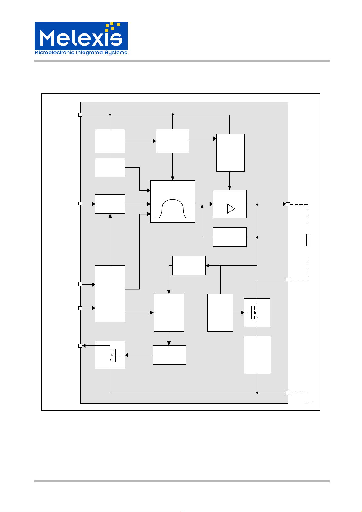
Functional Diagram
V
BAT
TH8055
Single Wire CAN Transceiver
TH8055
TxD
MODE0
MODE1
5V Supply
and
References
RC-Osc
Time Out
MODE
CONTROL
Biasing and
Monitor
V
BAT
Wave Sha ping
Input Filter
Receive
Comparator
Reverse
Current
Protection
CAN Driver
Feedback
Loop
Loss of
Ground
Detection
CANH
LOAD
RxD
RxD Blanking
Time Filter
Reverse
Current
Protection
GND
Figure 1- Block Diagram
390108055 Page 2 of 15
Rev. 1.1a
Jan 2002

Single Wire CAN Transceiver
Functional Description
TxD Input Pin - Logic command to transmit on the single wire CAN bus as follows:
TxD Polarity
TxD = logic 1 (or floating) on this pin produce an
undriven or recessive bus state (low bus
voltage)
TxD = logic 0 on this pin produce either a bus
normal or a bus high voltage dominant state
depending on the transceiver mode state (high
bus voltage)
If the TxD pin is driven to a logic low state while the
sleep mode (Mode0=0 and Mode1=0) is activated,
the transceiver not drive the CANH pin to the
dominant state.
Mode 0 and Mode 1 pins - are used to select transceiver operating modes:
The transceiver provides a weak internal pull down
current on each of these pins which causes the
transceiver to default to sleep mode when they are
not driven. The mode input signals are standard
CMOS logic level.
M0 M1 Mode
L L Sleep mode
H L High speed mode
L H Wake up
H H Normal mode
Sleep Mode
Transceiver is in low power state, waiting for wake
up via high voltage signal or by mode pins change to
any state other than 0,0. In this state, the CANH pin
is not in the dominant state regardless of the s tate of
the TxD pin.
High Speed Mode
This mode allows high speed download with bitrates
up to 100Kbit/s. The output waveshaping circuit is
disabled in this m ode. Bus transmitter drive circuits
for those nodes which are required to comm unicate
in high speed mode are able to drive reduced bus
resistance in this mode (see Table Static
The transceiver provides an internal pull up current
on the TxD pin which will cause the transmitter to
default to the bus recessive state when TxD is not
driven.
TxD input signals are standard CMOS logic levels.
Timeout Feature
In case of a faulty blocked dominant TxD input
signal the CANH output is switched off automatic ally
after the specified TxD timeout reaction time to
prevent a dominant bus.
The transmission is continued by next TxD L to H
transition without delay.
Characteristics). High speed communications shall
utilize the normal mode signal voltage levels as
specified in Static Characteristics.
Wake Up Mode
This bus includes a selec tive node awake capability,
which allows normal communication to take place
among some nodes while leaving the other nodes in
an undisturbed sleep state. This is accomplished by
controlling the signal voltages such that all nodes
must wake up when they receive a higher voltage
message signal waveform. The communication
system comm unic ates to the nodes inf or mation as to
which nodes are to stay operational (awake) and
which nodes are to put themselves into a non
communicating low power “sleep” state.
Communication at the lower, normal voltage levels
shall not disturb the sleeping nodes.
Normal mode
Transmiss ion bit rate in norm al comm unication is 33
Kbits/s. In normal transmission mode the TH8055
supports controlled waveform rise and overshoot
times. W aveform trailing edge control is required to
assure that high frequency components are
minimized at the beginning of the downward voltage
slope. The remaining f all time occurs after the bus
is inactive with drivers off and is deter mined by the
RC time constant of the total bus load.
TH8055
390108055 Page 3 of 15
Rev. 1.1a
Jan 2002

Single Wire CAN Transceiver
RxD Output pin - Logic data as sensed on the single wire CAN bus
RxD polarity
RxD = logic 1 on this pin indicates a bus
recessive state (low bus voltage)
RxD = logic 0 on this pin indicates a bus
normal or high voltage bus dominant state
RxD in Sleep Mode
RxD do not pass signals to the micro processor
while in sleep mode until a valid wake up bus
voltage level is received or the Mode 0,1 pins are
not 0,0 respectively. When the valid wake up bus
voltage signal awakens the transceiver, the RxD
Bus LOAD pin - Resistor ground with internal open-on-loss-of-ground protection
When the ECU experiences a loss of ground
condition, this pin switch to a high impedance state.
The ground connection through this pin is not
interrupted in any transceiver operating mode
including the sleep mode. The ground connection
only is interrupted when there is a valid loss of
ground condition.
V
INPUT pin - Vehicle Battery Voltage
BAT
The transceiver is fully operational as described in
Table Static Character istics over the range 5 < V
< 18 volts as measured between the GND pin and
BAT
pin.
the V
pin signalised an interrupt (logic 0) . However, if the
Mode 0 & 1 pins are at logic 0, the transceiver
returns to the sleep condition when the wake up bus
voltage signal is not present.
When not in s leep mode all valid bus signals will be
sent out on the RxD pin.
RxD will be placed in the undriven or off state when
in sleep mode .
RxD Typical Load
Resistance: 2.5 kohms
Capacitance: < 25 pF
This pin pr ovides the bus load resistor with a path to
ground which contributes less than 0.1 volts to the
bus offset voltage when sinking the maximum
current through one unit load resistor.
The transceiver’s maximum bus leakage current
contribution to VOL from the LOAD pin when in a
loss of ground state is 50uA over all operating
temperatures and 3.5 < VBAT < 18 volts .
For 0 < V
driven dominant) and RxD is undriven (high),
BAT
regardless of the state of the TxD pin (undervoltage
lockout).
< 5 volts, the bus is passive (not be
BAT
TH8055
390108055 Page 4 of 15
Rev. 1.1a
Jan 2002

CAN BUS input/output pin
Wave Shaping in normal and wake up mode
Wave shaping is incorporated into the transmitter to
minimize EMI radiated emissions. An important
contributor to emissions is the rise and fall times
during output transitions at the “corners” of the
voltage waveform. The resultant waveform is one
half of a sin wave of frequency 50 - 65 kHz at the
rising waveform edge and one quarter of this sin
wave at falling or trailing edge.
Wave Shaping in high speed mode
Wave shaping control of the rising and falling
waveform edges are disabled during high speed
mode. EMI emissions requirements are waived
during this mode. The waveform rise time in this
mode is less than one µs.
Short circuits
If the CAN BUS pin is shorted to ground for any
duration of time, an over temperature shut down
circuit disables the output high side drive source
transistor before the local die temperature exceeds
the damage limit threshold.
TH8055
Single Wire CAN Transceiver
Loss of ground
If the CANH voltage decreases under the specified
value below the ECU - ground, the LOAD pin is
switched into high impedance state. The CANH
transmission is continued until the undervoltage lock
out voltage threshold is detected.
Loss of battery
In case of loss of battery (VBAT = 0 or open) the
transceiver do not disturb bus communication. The
maximum reverse current into power supply system
doesn‘t exceed 500µA.
390108055 Page 5 of 15
Rev. 1.1a
Jan 2002
 Loading...