

MELEXIS TH8052.2 Datasheet

Features and Benefits
TH8053
www.melexis.com
Page 1 Datasheet Rev 1.2 Nov 2000
Baud rate up to 125k Baud
Up to 40 nodes can be connected
Automotive temperature range from -40°C...125°C
Very low standby current
Short circuit protection of bus lines to V
DD
, ground and battery
Wake up capability from bus line or wake up pin
Supports unshielded bus wire
Integrated receiver filters
Permanent dominant monitoring of transmit data input
Automatic switching to single wire mode in case of bus failures and automatic reset to differen-
tial mode if bus failure disappeared
One wire transmission mode with ground offset up to 1.5V possible
Very low RFI due internal slope control of bus drivers
Good immunity to EMC
Thermal pr ot ec ti o n o f bus line dri ver s
Ordering Information
Part No. Temperature Rang e Package
TH8053.2 -40ºC...125ºC SOIC14, 150mil
Fault Tolerant Low Speed CAN Transceiver
Pin Diagram
TH8053
1
2
3
4
14
13
12
11
INH VBAT
NERR
RXD
TXD
CANH
CANL
GND
5
6
7
STB
WAKE
EN
10
9
8
RTH
RTL
VDD
SOIC14NB
General Descri ption
The TH8053 is a fault tolerant CAN-Transceiver which
wor ks a s an int erf ac e bet ween t he C AN pro toc ol c ont rol ler and the physical CAN bus. It is designed to connect
up to 40 control nodes in passenger cars with an overall
cable length of up to 80m enabling data trans-mission/
reception rates up to 125
kBaud using unshielded bus
wires.
In normal operation mode the device supports the high
security differential transmit capability of the differential
CAN bus. In the recessive state data coming from the
bus is filtered and after converting to a single-ended sig-
nal fed to the RXD output pin that is to be connected to
the CAN controller (reception of data). In the dominant
stat e d at a send fr om t he co ntr oll er to pi n TX D dri ves th e
CAN bus lines.
The device automatically switches to an appropriate single en d ed m od e i n t h e c as e of a b u s fa il ur e en s u r i n g f ur ther function of the l network. If the failure gets removed
the TH8053 automatically resets itself to normal operation. Furthermore it enables single ended transmission
on wires with a ground shift up to 1.5V. The TH8053 also
ensu res t he dat a tran sfer if the s ystem c ont ains a si ngl e
TH8053
Fault Tolerant Low Speed CAN Transceiver
www.melexis.com
Page 2 Datasheet Rev 1.2 Nov 2000
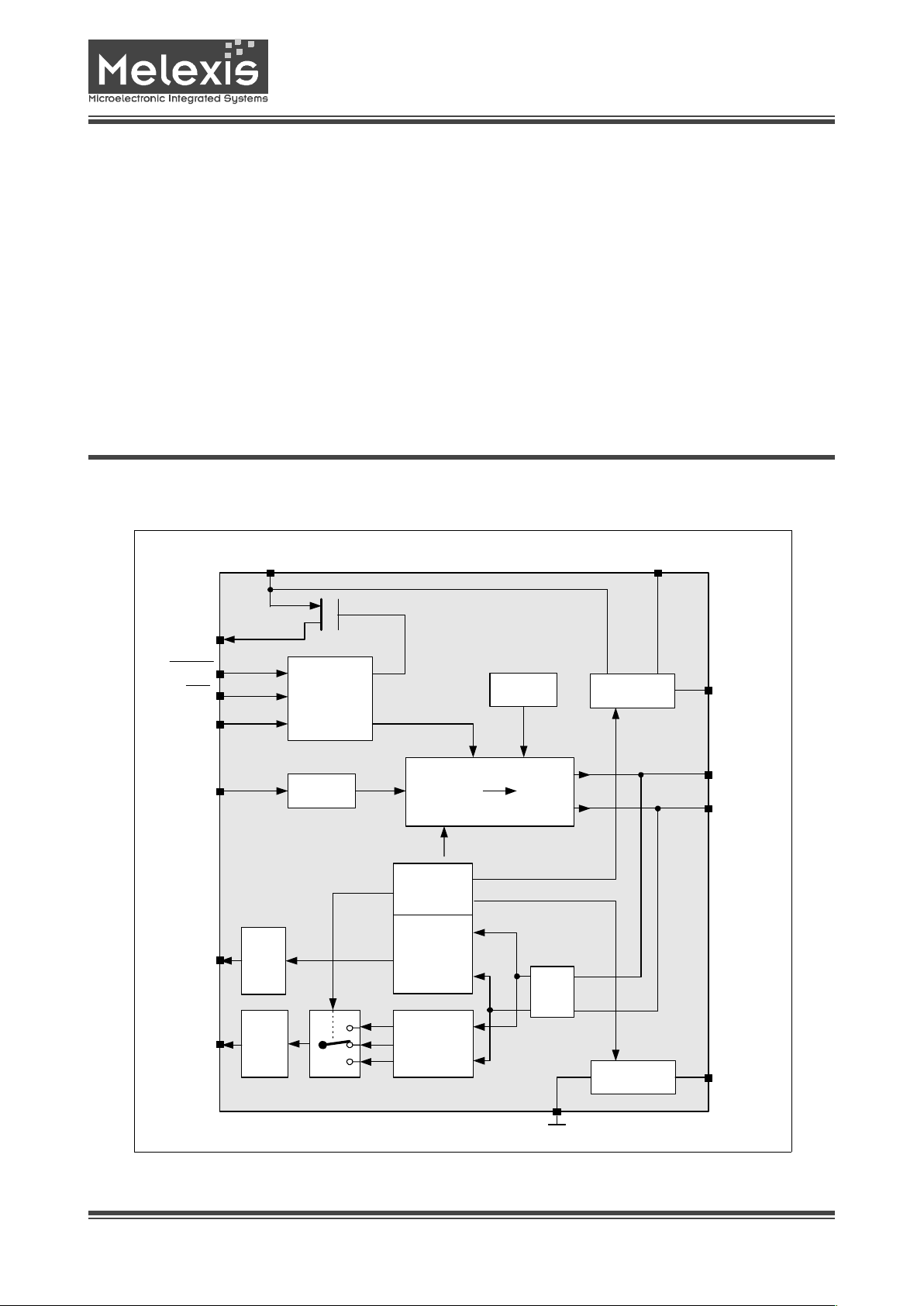
Functional Diagram
Wake- up
Standby/Sleep
Control
Timer
Temperature
protection
Failure
management
Filter
Receiver
Output
stage
H-
Termination
1
INH
Slope
control
Driver
stage
Output
stage
7
5
6
2
WAKE
STB
EN
TXD
4
NERR
3
RXD
13
GND
RTH
8
CANL
12
11
CANH
9
RTL
10
VDD
14
VBAT
Failure
detection
Wake- up
Time- out
L-Termination
General Descri ption (continued)
unpowered node (e.g. a missing termination resistor).
Another feature added is the monitoring of the TXD-input
to prevent the controller from obstructing the CAN bus by
sending a permanent dominant state. The presence of
any of these err ors is indi cated by a LOW-si gnal at th e
NERR-pin.
Standby and sleep modes enable low current consumption if no transmit capability is needed or if the supply
voltages drop under a specified level. A wake-up function
recalls the normal operation mode whenever a slope is
detected at the WAKE-Pin or transmission of data on th e
bus occurs.
Other important features within passenger cars are the
low RF-interference due to a limitation of rise and fall
slopes as well as the insensitiveness to RF-radiation
achieved by integrated rece ive r filters.
A thermal shut-down circuit prevents the TH8053 from
any damage caused by increased power consumption of
the C AN out put st ages while al l ot her pa rts of t he cir cui t
remain working. Furthermore the TH8053’s bus connections (CANH, CANL) are short-circuit proof to battery and
ground voltage as well as any pin is protected against
ESD-Events.
Figure 1 - Block Diagram

TH8053
Fault Tolerant Low Speed CAN Transceiver
www.melexis.com
Page 3 Datasheet Rev 1.2 Nov 2000
The s i g nal c om i ng f r om th e d i ff er en t i al C AN b u s i s f ed t o
a fil ter stag e to inh ibit hig h freq uenci es t hat i nter fere t h e
bus line from disturbing the evaluation of the incoming
bus data. The cut-off frequency of the filters has to be regarded as a trade-off between RF-suppression and
propagation delay.
The failure detection circuit determines whether one of
the f ail ures desc ri bed in Tabl e 1, “ CAN b us fa ilur es, ex ists and indicates a present error as an active LOW at
the NERR output. Furthermore the information of the
kind of failure is given to the failure management block
which takes the appropriate measures to ensure transmission and reception of data. This includes the control
of t he co rr ec t t erm i n ati o n of th e CA N bu s l i nes a s w el l a s
the choice of the right derivation of the receiver signal
(output to the RXD-pin) from the CANH and CANL inputs. The failure management also contains the possibility to di sa ble o ne of th e dri v er sta ges (e. g. in the ca se o f
fai l ur e 6 th e hi g h si d e dr iv er a nd t he R T H term i n at io n a r e
disabl ed to reduce c urrent consumption). D uring any kind
of single-wire data transfer RF-radiation and RFsensitivity are increased.
The failure detection consists of two detection circuits,
one being active in the normal operation mode and the
other one working in the standby and sleep modes. Recovery of the failures is done with a certain time-out that
depends on the failure. A wake-up function that detects
incoming dominant signals from the bus is also included.
A wake-up command can also be generated by changing
the logical voltage level at the WAKE-pin. The mode the
TH8053 is running within and whether the INH-pin disables an external voltage regulator can be controlled by
the EN- and STB-pins as shown in Table 3, “Mode Control, on page 4 and detailed described in “Operation
Modes” on page 4
Another feature implied in this can transceiver device is
Depending on the occurring error appropriate measures
have to be taken to ensure data transmission and reception. Table 2, “Error Management”, lists the means to
achieve this target in the normal operation mode. The
comparator signal that determines the value of RXD is
given in the second column, the third and fourth ones
con tain th e inf ormati on whet her eith er one of th e termi nations RTH or RTL is switched off to reduce the current
flowing in the termination resistances. The last two columns display if one of the transmitter drivers is deactivated.
If an interr upt of the CANH or CANL wir e between two
ECUs is detected (failures 1 and 2) there is no need to
disable the corresponding high or low side driver because differential transmission towards other ECUs may
still be useful.
Error Management
______________________________
1
If the termination is switched off, a current of 75µA is supplied at the RTH -or RTL-pin.
2
Low side driver is switched off after two unsuccessful attempts of reaching dominant level.
Table 2 - Error Management
Errors 1 and 3a as well as errors 2 and 4 can’ t be distingu is h ed
by the recei ver.
Error
Output
to RXD
Termination1
RTH RTL CANH CANL
1 D on on on on
2 D on on on on
3 H on off on off
2
3a D on on on on
4 D on on on on
5 H on off on off
6 L off on on on
6a L off on on on
7 H on off on off
Driver
Nr.
Failure description Condition
1 CANL wire interrupted
2 CANH wire interrupted
3 V
BAT
>7.2
3a V1.8V<V
BAT
<7.2V
4 CANH shor t- c irc u ited to grou nd
5 CANL short-circuited to ground
6
CANH sh ort- c ir c u it ed to batter y
suppl y volt ag e
V
BAT
>7.2 V
6a 1.8V<V
BAT
<7.2V
7 CANH short-circuited to CANL
CANL short-circuited to battery
suppl y volt ag e
Table 1 - CAN bus failures
(Definition in accordance with ISO 11519-2)
Functional Description (continued)
the t ime-o ut cir cuit at t he TXD-I nput t hat prev ents oc cupation of the CAN bus by a long-term dominant signal
sent from the CAN controller. If no failure occurs the
TXD-signal coming from the CAN controller is fed to the
driver stage which includes a limitation of slopes to reduce RF-interference caused by radiation on the CAN
bus.
To prevent the chip from a thermal breakdown a temperature protection circuit shuts down the driver stages
whi c h r epr es en t th e b ig g est part of t he w h ol e po w er con sumption. All other parts remain active thus a reception
of data is still possible. After cooling down and reaching
the low temperature level the transmitter will be enabled
again.

TH8053
Fault Tolerant Low Speed CAN Transceiver
www.melexis.com
Page 4 Datasheet Rev 1.2 Nov 2000
______________________________
1
Wake-up interrup ts ar e rel eased when t h e norm al operation mode is entered
2
Sleep mod e wi ll b e entered instead of V
BAT
-standby m od e if th e go-to-sleep c om m and was applied before. (EN m ay turn LOW as VDD drops
without affecting internal functions because of fail safe functionality.)
3
The "missing V
BAT
" flag will be reset t o HIGH when the n orm al operation mode is entered
Power-on Procedure
The different operation modes can be selected by the
signals provided at the EN- and STB-pins. There are
three operation modes which enable reduced power consumption: the sleep mode, th e V
BAT
-standby mode and
the V
DD
-standby mode.
The s leep m od e (S TB=0 , E N=0) is t he o ne wi th the l o west power consumption because the whole chip and
even the external voltage regulator get disabled. This
mode can only be reached if an intermediate mode
(STB=0, EN=1) is entered which is interpreted as a “goto-sleep”-command. Otherwise the chip switches to the
V
BAT
-standby mode (STB=0, EN=0) where the external
voltage regulator remains further active. In these modes
(go-to-sleep, sleep, V
BAT
-standby) the RTL-pin is
switched to V
BAT
.
If t he ext er nal in hibi t abl e vol ta ge r egul at or i s not th e on e
that provides the V
DD
-supply voltage or if the device is
operating in the V
BAT
-standby mode (external voltage
regulator is active) a wake-up request from either the
WAKE-pin or the CAN bus line is visible as an active
LOW at the NERR and RXD outputs. If V
DD
has been
swi tched of f in the sl eep mo de the wa ke-up r equest w ill
cause the TH8053 to enter the V
BAT
-standby mode as an
intermediate state in which the V
DD
-supply is present
again and so the wake-up can be observed at the NERRand RXD-pins as well.
Operation Modes
Table 3 -Mode Control
/STB EN Mode INH
NERR RXD
RTL
0 0 V
BAT
-standby1 high V
BAT
switched to V
BAT
0 0 sleep
2
floating switched to V
BAT
0 1 go-to-sleep command floating switched to V
BAT
1 0 V
DD
-standby3 high/ V
BAT
active LOW
missing V
BAT
flag
active LOW
wake-up interrupt
switched to V
DD
1 1 normal operation high/ V
BAT
active LOW
error f lag flag
HIGH = recessive bus;
LOW = dominant bus
switched to V
DD
active LOW wake- up interrupt signal if V
DD
is
present
Another mode is the VDD -standby mode (STB=1, EN=0).
Similar to the normal operation mode the RTL-pin is
switched to V
DD
. The appearance of a wake-up condition
in this mode is only displayed at the RXD output as an
active LOW. The NERR output is used to indicate the
drop of V
BAT
below 1V. This warn flag is necessary to
show that V
BAT
was missing and that a reinitialisation has
to be done. It is reset to HIGH when the device enters
the normal operation mode in which the NERR-pin is
used to indicate bus failures.
During the low power modes (sleep, V
BAT
- and VDDstandby) the detection of errors is reduced to the monitoring of the appearance of failures 5, 6 and 7. A complete deactivation of the detection circuit is not senseful
beca use th e occurr ence of failur es 5, 6 and 7 w ould result in an increased power consumption.
The TH8053 switches itself to the V
BAT
-standby mode if
V
DD
is missing or below the thresh-old. If VDD is missing
the EN and STB inputs will be held internally at LOW
lev el to pr event t he chip fr om enter ing an i nappro priat e
mode (fail safe functionality). In all standby modes the
TH8053 is able to receive interrupts. During the first time
of the go-to-sleep command and the specified time after
switching from the normal operation mode to the standby
modes the device ignores an interrupt.
flag that it has to reinitialize the ECU (e.g. after exchanging the complete CAN unit or after a battery voltage
breakdown).
Through entering the normal mode the VBAT low flag will
be reset. Due to special output stages the CAN bus is
not loaded if V BAT = 0V which ensures data transmission on the CAN bus even if some ECUs are unpowered.
The chip automatically enters the V BAT -standby mode
because of its fail safe functionality. In the V BAT standby mode the INH output will become HIGH and
ther efore the volt age regul ator will provi de V
DD
-supply.
The CAN transceiver will remain in the V
BAT
-standby
mode until the CAN controller sets it to another mode.
The controller should first enter V
DD
-standby Mode. This
way the CAN controller will be shown by the power-on
TH8053
Fault Tolerant Low Speed CAN Transceiver
www.melexis.com
Page 5 Datasheet Rev 1.2 Nov 2000
All voltages are referenced to ground (GND). Positive
currents flow into the IC. The absolute maximum ratings
(in accordance with IEC 134) given in the table below are
limiting values that do not lead to a permanent damage
of the device but exceeding any of these limits may do
Electrical Characteristi cs
Abso lute maximum ratings
______________________________
1
t < 500ms; load dump
2
V
DD
=0 to 5.5V; V
BAT
>0 V; t<0.1; no time limit
3
V
DD
=0 to 5.5V; V
BAT
>0 V; t<0.1 ms; l oad du m p
4
For a hum an b od y mod el ( equ i val en t t o dis c h arging 100pF wit h 1.5kΩ).
5
For a hum an b od y mod el ( equ i val en t t o dis c h arging 100pF wit h 1.5kΩ).
6
Junction temperature is defined in IEC 747-1
Parameter
Symbol Min Max Unit Notes
DC supply voltage VCC -0.3 +6.0 V
Battery voltage V
Bat
-0.3 +27
V
40
1
DC Input voltage at pins 2 to 6 V
2-6
-0.3 VCC + 0.3 V
CANH, CANL input voltage V
CANH,L
-10 27
V
2
-40 40
3
CANH, CANL transient input voltage V
CANH, L, tran
-150 100 V
Termination resistance at pins 8 and 9 R
TH, RTL
500 16000
Ω
DC input voltage at pin 1, 8, 9 V
1,8,9
-0.3 V
BAT
+0.3 V
DC input voltage at pin 7 V
WAKE
V
BAT
+0.3 V
DC input current at pin 7 I
WAKE
-15 mA
Maximum latch-up free current at any pin I
Latch-up
-500 +500 mA
Electrostatic discharge voltage at any pin V
ESD
-2000 +2000 V
4
Storage temp erature r ange T
STG
-55 +150 °C
Junction temperature T
Junc
-40 +150 °C 6
Thermal Resistance from junction to ambient R
Th
120 K/W
so. Long ter m expo sure t o limi ting v alues m ay aff ect the
reliability of the device. Reliable operation of the TH8053
is only specified within the limits shown in ”Operating
conditions”
Operating Conditions
Parameter Symbol Min Max Unit Notes
DC supply voltage VDD 4.75 5.25 V
Battery voltage V
BAT
6 27 V
Operating am bient temp erature T
amb
-40 +125 °C
Junction temperature T
junc
-40 +150 °C 6
 Loading...