

MELEXIS TH7301 Datasheet
TH7301
Dual-Channel Programmable
Low-Pass Filter
Description
Features
Applications
The device incorporates two matching 4th-order
Butterworth filters with voltage gain control to
perform low-pass filtering on quadrature demodulated signals. The cutoff frequency and inband
gain are programmable via a standard 3-wire
interface. The cutoff frequency can be set between
0.8 MHz and 22.4 MHz and the inband voltage
gain can be set between -3 dB and 20 dB. The
cutoff frequency value is determined via a 10-bit
control word, with smaller step sizes in the lower
Wide cutoff frequency range (0.8 MHz to
22.4 MHz)
Dual-channel architecture produces superior
matching and ease of us e for quadrature signals
Companding design provides higher resolution at
lower cutoff frequencies
Digital Broadcasting Systems (DBS) and
Digital Video Broadcasting (DVB)
Satellite and cable TV decoders
Microwave point to point links
portion of the cutoff frequency range. The device
contains an on-chip oscillator to adjust the cutoff
frequency. Maintaining amplifiers configure the
Butterworth filter as the phase shift component of
the oscillator. The frequency of oscillation tracks
the filter cutoff frequency. The cutoff frequency of
the filter can be accurately set according to the
resolution of the IC by measuring the frequency of
oscillation.
Low power consumption (<105 mA, typical 55 mA
from -5 V supply; Fc = 1 MHz @ 25°C)
Single ended or differential input operation
possible (AC coupled)
No external components for trimming necessary
Small package (16-pin SOP)
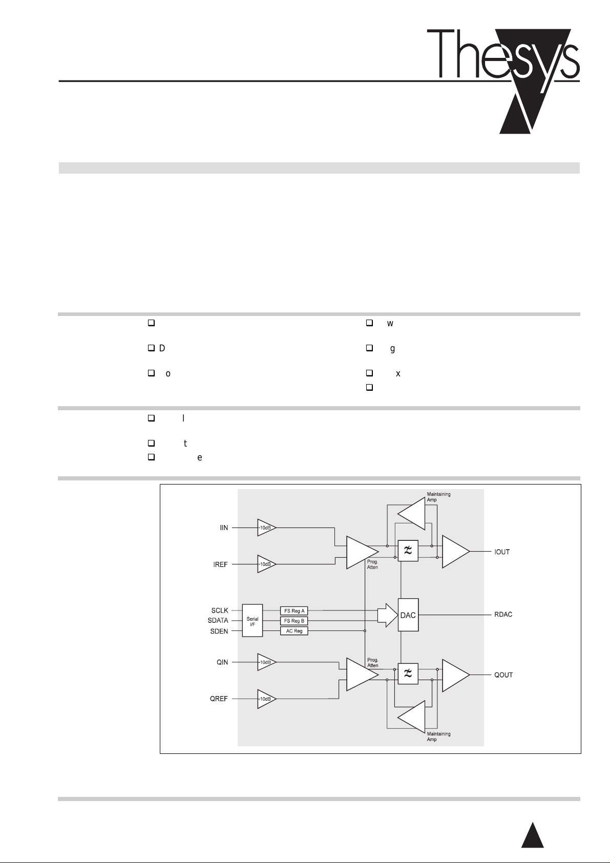
Block Diagram
Figure 1: Block Diagram
4th Order
Butterworth
Filter
4th Order
Butterworth
Filter
Fixed Gain
Fixed Gain
Rev. 2.1
November 1999

TH7301 Dual-Channel Programmable Low-Pass Filter
Theory of
Operation
The IC is divided into I an d Q channel signal
paths each consisting of an input stage, gyrator
4th order Butterworth low-pass filter, output stage
and feedback amplifier for an oscillator. A serial
interface is provided to allow the gain and cutoff
frequ ency to be program med via a st andard 3
wir e in t er face. Th e digital cutoff frequency sett i ng
is converted to a current by a digital-to-analog
conver ter. In ternal bandgap references and
biasing blocks provide top level biasing on voltage
and current refer ences for the complete device.
Input stage
The device incorporates programmable attenuation in the input stages to maintain filter linearity
and to provide overall gain contro l for the IC. The
attenuation can be programmed in coarse steps
of 3 dB with fine control of 0.5 dB in the input
tran sconductor of th e gyrator filter s. Internal
multiplexers and back to back followers allow
sin gle-ended or differ ential input oper ation on both
I and Q signal paths.
4th order Butterworth filter
The filter architecture is based on a fully balanced
continuous time gyrator technique with 4th or der
Butterworth response. Linear current programmab le t ranscon ductance elements are us ed to
synthesise the two inductors and source and
terminat ion impedance of the fi lter. A t er min ation
to source impedance ratio of 2:1 is selected to
mi nimise out put noise while m aintainin g a
realisab le ra nge of capacitor values.
The use of a differential architecture has three
distinct advanta ges. Firstly the ultimat e noi se
rejection is substantially better than that of the
unbalanced LC fi lter. Secondly differ ential drive
allows the use of a current programmable Gm
stage with very much greater signal handling. And
finally DC loading of the output is common mode
and does not lead to differential DC offsets. This
last point is especially important as the bias
current within the filter can become very low at
low cutoff frequencies.
Out put stage
The output stage is designed to carry out differential
to si ngle ended conver sion and provi des the
capability of driving up to 15 pF of capacitive load.
Oscillator
The maintaining and limiting amplifier i s used as
part of a phase shift oscillator circuit with the
gyrator But terworth filter as the phase shift
element. The frequency of oscillation occurs at t he
-3 dB fr equency of t he filter as the phase shift
thr ough a 4t h order Butterwor th fi lter is 180
degrees at the -3 dB poi nt. Vo ltage limi ters are
integrated into the gyrator filters and limit the
differential voltage to 50 mVpp in order to ensure
that the transconductance elements remain in
their l inear reg ion of operation and henc e the
expected inductance values are synthesised.
Serial interface
Th e fi lt er cutof f frequency and gain are programmed via a 3 wi re serial interf ace bus. The in t er face
consists of the serial data clock (SCLK), serial
data input (SDATA) and a serial enable (SDEN).
The filter is progra mmed b y asserting SDEN and
clocking the 8 bit serial data, MSB first, into the
shift register. The two most significant bits
represent the register address bits. The 6 LSB of
data are loaded into the relevant register on the
falling edge of SDEN.
The serial interface consists of: an 8 bit serial
input to parallel output (SIPO) register, three 6-bit
parallel load registers and register address
decode logic.
Once S DEN is asserted, data is clocke d in to the
SIPO on the positive edge of SCLK. When the
data is loaded, the two address bits are decoded
to determine which register should be updated.
The data is transfered to the register on the falling
edge of SDEN.
The serial interface does not contain a power on
reset, thus all three registe rs must be programmed
before reliable filter operation can be achieved.
DAC
The digital - to-a nalog converter is used to select
the filter cut off frequency via a programma ble
refe rence current. The fully companding DAC
div i des the fr equency range i nto 5 chor ds, each
wit h 128 equal fr equency steps. The reference
curr ent is pr ogrammed by an external resisto r
placed between RDAC and Vee. The final output
is mirrored for the I and Q channels to provide
isolation.
The chords are select ed by a 3 bit w ord and th e
frequ ency step by a 7 bit word. The com panding
law i s gener ated by adding th e chord curr ents and
dividing t he required ch ord into 128 step currents .
2
TH7301 Dual-Channel Programmable Low-Pass Filter
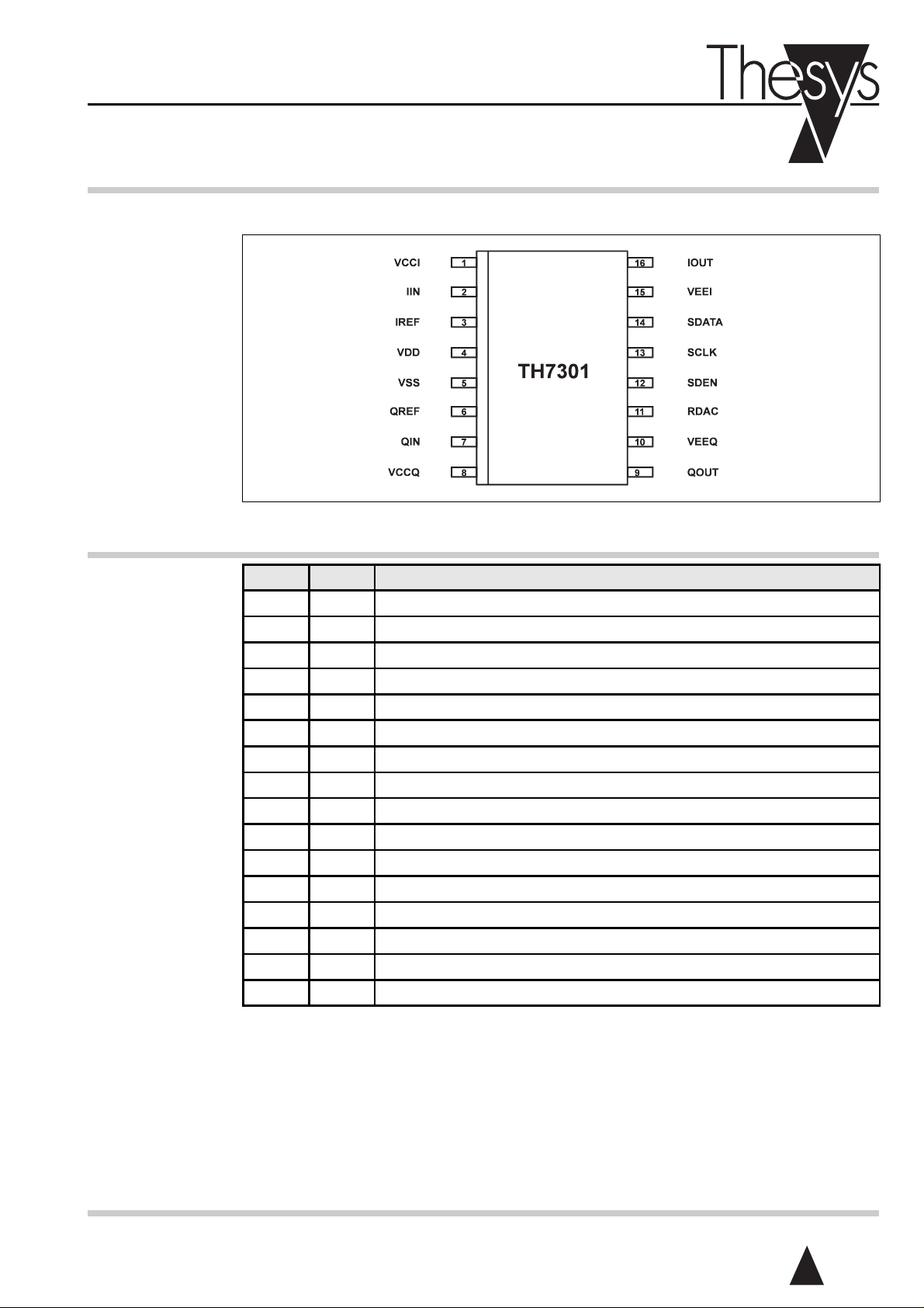
Pinout
Information
Pin Definition List
The TH7301 is contained i n a plast ic 16 pin SOP package.
Figure 2: Pinout Schematic
Pin No. Symbol Function
1 VCCI I channel positive supply
2 IIN I channel signal input
3 IREF I channel signal reference
4 VDD Digital positive supply
5 VSS Digital negative supply
6 QREF Q channel signal reference
7 QIN Q channel signal input
8 VCCQ Q channel positive supply
9 QOUT Q channel output
10 VEEQ Q channel negative supply
11 RDAC DAC referen c e curr en t s etting res i s tor connec t s between t his pin and negat ive rail
12 SDEN Serial data enable
13 SCLK Serial data clock
14 SDATA Serial data input
15 VEEI I channel negative supply
16 IOUT I channel output
3
TH7301 Dual-Channel Programmable Low-Pass Filter
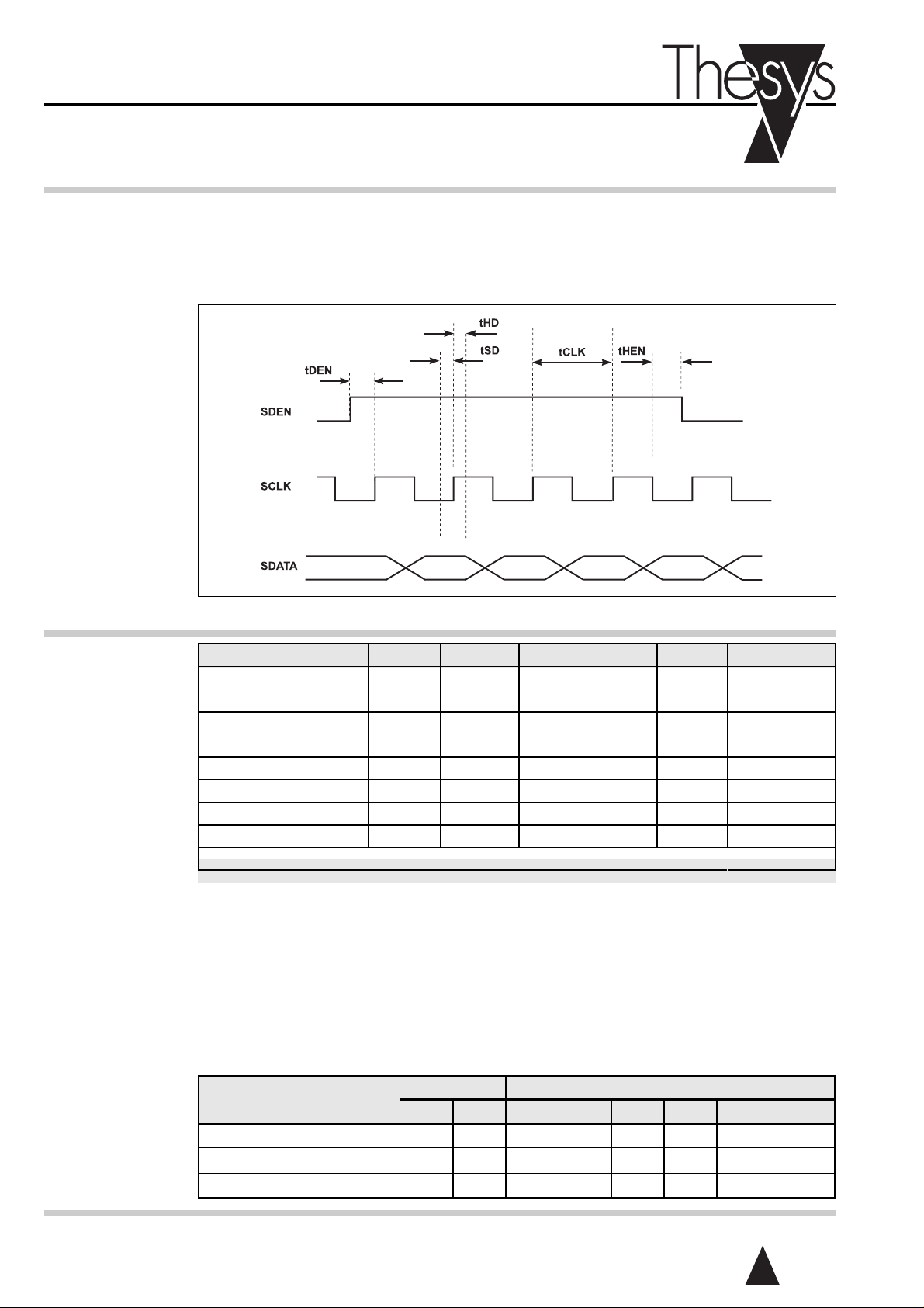
Serial In t erf ace
Programmin g
Operating
conditions
for the 3 wire
interface
The seria l inter face is a 3- w ire bus used to
program t he f ilt er cutoff frequency and volt age
gain. Pin SDATA is the serial data input for an 8bit s hift r egister, S CLK is the shift reg ister clock
(active positive ed ge), SDEN (ac tive high) is the
referenced to a - 5 V sup ply and that th er e is no
global reset for the logic devices, so a reset word
should be input after power up.
The timing diagram for the interface is shown
below.
serial inte r fac e enab le. Note that logic le vels are
Figure 3: Serial Interface Tim ing Diagram
Parameter Symbol Min Typ Max Unit Comments
Power supply voltage VSS -5.25 -5.0 -4.75 V relative to VDD
High level input voltage VIH 0.3 * VSS VDD + 0.1V note
Low level input voltage VIL VSS - 0.1V 0.7 * VSS note
Serial data clock period tCLK 50 ns
Serial data setup time tSD 10 ns
Serial data hold time tHD 10 ns
Serial data enable delay time tDEN 20 ns
Serial data enable hold time tHEN 20 ns
Notes: Logic threshold levels for inputs SCLK, SDATA and SDEN. Note that this is a negative supply IC.
The serial data is stored in one of 3 intern al
registers - gain control, frequency select A and
frequ ency select B.
The first two bits of the serial data form an
address code for the regist er s. The gain control
bits AC(5...0) are deco ded to sele ct a voltage gain
betw e en 0 dB and 20 .5 dB in 0.5 dB st eps. The
frequency select bits FC(2...0) select one of the
octave chords while FS(6...0) select the step
within each chord.
Usage
Frequency Select A 0 0 FS2 FS1 FS0 FC2 FC1 FC0
Frequency Select B 0 1 OS0 0 FS6 FS5 FS4 FS3
Gain Control 1 1 AC5 AC4 AC3 AC2 AC1 AC0
Address Bits Data Bits
D7 D6 D5 D4 D3 D2 D1 D0
Additional bit OS0 (active high) controls the
oscillator (for test issues only). The table below
shows t he address and da ta decodi ng of the seri al
data input.
The serial interface does not contain a power on
reset, t hus all three registers must be programmed after power on to prevent undefined
logical state s and to achieve reliable filte r op eration. I. e. a first reset word may reset all registers
to 0.
4
TH7301 Dual-Channel Programmable Low-Pass Filter
f
Definition of
Terms
- cutoff frequency setting
cset
f
- cutoff frequency (-3dB bandwid t h)
c
f
-step size
step
Av- voltage gain
Frequency
Setting
To maintain frequency resol ution at low frequencies a companding la w i s appli ed to the frequency co de. The frequency range is sel ected as
one of the five octaves in the total filter range
controlled by bits FC(2...0). Each octave is divided
linearly into 128 equ ally si zed steps decoded by
bits FS(6...0). This frequency range is for an
external r esistor value of 4.5 kΩ between pin
RDAC and VE E. The rang e is design ed t o
guarantee 0.8 MHz to 22.4 MHz cut off ra ng e,
taking process variations in top account without
the need to change this external resistor. If there
is a need to fine tune t his fr equency range for any
reason, it may be re-centered by selecting a
suit ably valued external r esistor.
The 12 8 st eps within ea ch octave are decoded by
FS(6...0). The according control mechanism
applies identically to all octaves refering to the
appropriat e step sizes of each oct ave, as shown
in the tables an d t he example bel ow.
Example:
FC(2...0) = 000
(frequency range 0.8 ... 1.5937 MHz,
Step size = 6.25 kHz)
FS(6...0) = 000001 1
f
= 0.81875 MHz
cset
The tabl es below show the selectable frequency
settings.
FC
(2..0)
000 0.8 ... 1.5937 6.25
001 1.6 ... 3.1875 12.5
010 3.2 ... 6.375 25
011 6.4 ... 12.75 50
1xx 12.8 ... 25.5 100
FS
(6...0)
0000000 0 fcset = fmin
0000001 1 fcset = fmin + fstep
0000010 2 fcset = fm in + 2*fstep
0000011 3 fcset = fm in + 3*fstep
.
.
.
1111111 127 fcset = fmin + 127*fstep
Frequency range
fmin ... fmax (MHz)
Cutoff Frequency
Step N
.
.
.
fcset = fmin + N*fstep
Step size
fstep (kHz)
(MHz)
.
.
.
Gain Setting
The ga in con trol bits A C( 5. ..0) are decoded to
select a volta ge gain between -3 dB and 20.5 d B
in 0. 5 dB steps. The gain control is divid ed i nto 8
steps controlled by AC(2...0) with additive step
sizes of 0.5 dB decoded by AC(5...3).
For example, to set the gain to 16 dB
AC(5...0) = 011001.
The tabl e below shows t he gain setting.
AC(2...0) Gain (dB) AC(5...3) Gain (dB)
000 18 000 2.5
001 15 001 2.0
010 12 010 1.5
011 9 011 1.0
100 6 100 0.5
101 3 101 0.0
110 0 110 0.0
111 -3 111 0.0
5
 Loading...