

TH7122
27 to 930MHz
FSK/FM/ASK Transceiver
Features
Single chip solution with only a few external
components
Stand-alone fixed-frequency user mode
Programmable multi-channel user mode
Low current consumption in active mode and
very low standby current
PLL-stabilized RF VCO (LO) with internal
varactor diode
Lock detect output in programmable
user mode
On-chip AFC for extended input frequency
acceptance range
Ordering Information
Part Number Temperature Code Package Code Delivery Form
3wire bus serial control interface
FSK/ASK mode selection
FSK for digital data or FM for analog signal
reception
RSSI output for signal strength indication and
ASK reception
Peak detector for ASK detection
Switchable LNA gain for improved dynamic
range
Automatic PA turn-on after PLL lock
ASK modulation achieved by PA on/off keying
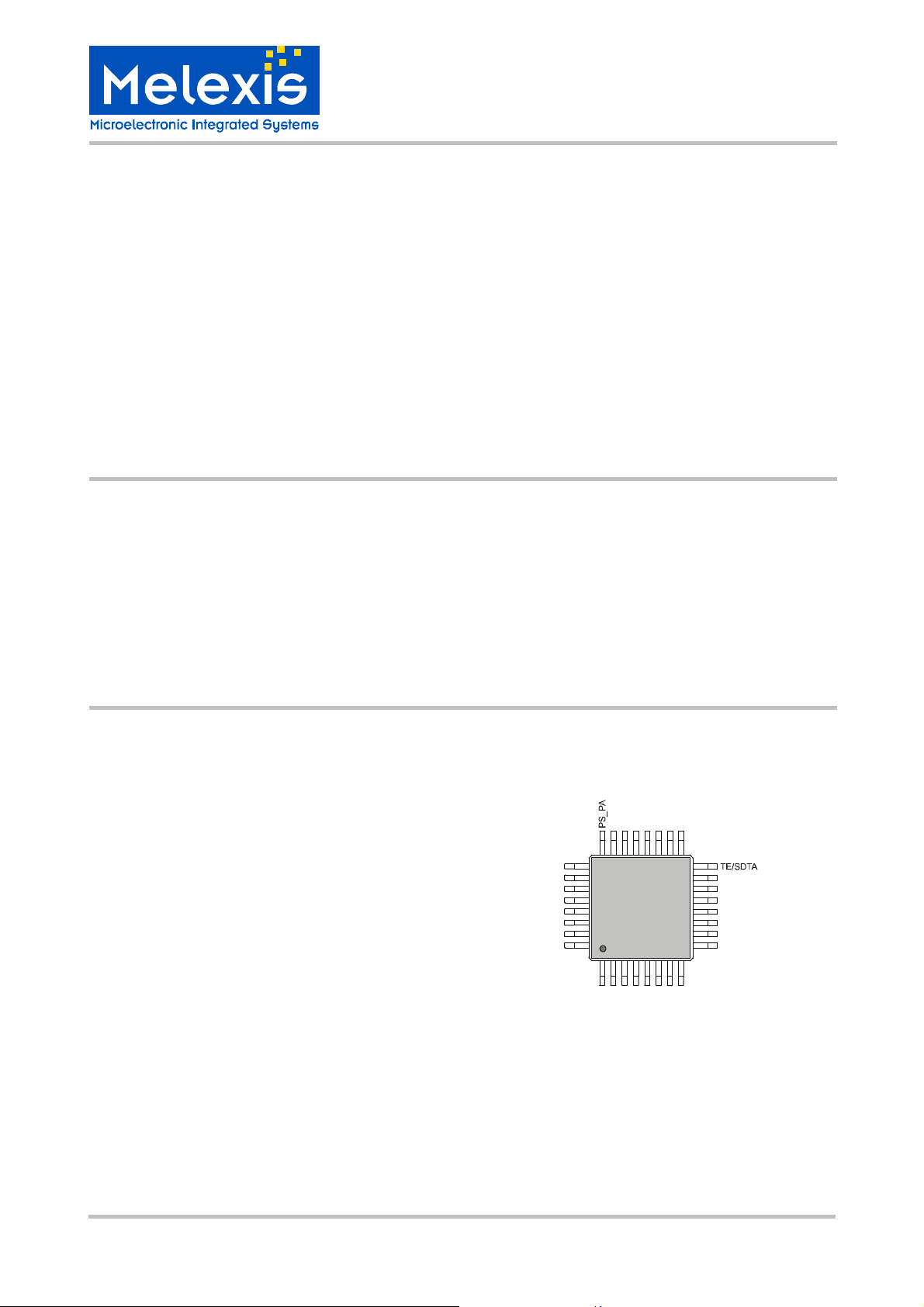
32-pin Low profile Quad Flat Package (LQFP)
TH7122.1
(only for existing designs,
E (-40 °C to 85 °C) NE (LQFP32)
not for new design-ins)
TH7122.2
(for new design-ins)
E (-40 °C to 85 °C) NE (LQFP32)
Application Examples
General bi-directional half duplex digital data
RF signaling or analog signal communication
Tire Pressure Monitoring Systems (TPMS)
Remote Keyless Entry (RKE)
Low-power telemetry systems
Alarm and security systems
Wireless access control
Garage door openers
Networking solutions
Active RFID tags
Remote controls
Home and building automation
250 pc/tray
2000 pc/T&R
250 pc/tray
2000 pc/T&R
Pin Description
OUT_PA
IN_LNA
VEE_LNA
OUT_LNA
GAIN_LNA
IN_MIX
VEE_IF
OUT_MIX
24
25
TH7122
32
1
IN_IFA
LF
TNK_LO
INT2/PDO
FS0/S DEN
VCC_PLL
FS1/LD
VEE_DIG
17
16
9
8
INT1
RSSI
OUT_DTA
OUT_DEM
VEE_PLL
VCC_IF
IN_DEM
RE/SCLK
VCC_DIG
ASK/FSK
IN_DTA
FSK_SW
RO
VEE_RO
General Description
The TH7122 is a single chip FSK/FM/ASK transceiver IC. It is designed to operate in low-power multichannel programmable or single-channel stand-alone, half-duplex data transmission systems. It can be used
for applications in automotive, industrial-scientific-medical (ISM), short range devices (SRD) or similar applications operating in the frequency range of 300 MHz to 930 MHz. In programmable user mode, the transceiver can operate down to 27 MHz by employing an external VCO varactor diode.
39010 07122 Page 1 of 44 Data Sheet
Rev. 010 Feb/09

TH7122
27 to 930MHz
FSK/FM/ASK Transceiver
Document Content
1 Theory of Operation...................................................................................................4
1.1 General............................................................................................................................. 4
1.2 Technical Data Overview.................................................................................................. 4
1.3 Note on ASK Modulation .................................................................................................. 4
1.4 Block Diagram.................................................................................................................. 5
1.5 User Mode Features......................................................................................................... 5
2 Pin Definitions and Descriptions..............................................................................6
3 Functional Description ............................................................................................10
3.1 PLL Frequency Synthesizer ........................................................................................... 10
3.1.1 Reference Oscillator (XOSC)..................................................................................................... 11
3.1.2 Reference Divider...................................................................................................................... 11
3.1.3 Feedback Divider....................................................................................................................... 11
3.1.4 Frequency Resolution and Operating Frequency...................................................................... 11
3.1.5 Phase-Frequency Detector........................................................................................................12
3.1.6 Lock Detector............................................................................................................................. 12
3.1.7 Voltage Controlled Oscillator with external Loop Filter.............................................................. 13
3.1.8 Loop Filter.................................................................................................................................. 13
3.2 Receiver Part.................................................................................................................. 13
3.2.1 LNA............................................................................................................................................ 14
3.2.2 Mixer .......................................................................................................................................... 14
3.2.3 IF Amplifier.................................................................................................................................14
3.2.4 ASK Demodulator...................................................................................................................... 14
3.2.5 FSK Demodulator ...................................................................................................................... 15
3.3 Transmitter Part.............................................................................................................. 15
3.3.1 Power Amplifier.......................................................................................................................... 15
3.3.2 Output Power Adjustment.......................................................................................................... 16
3.3.3 Modulation Schemes................................................................................................................. 16
3.3.4 ASK Modulation......................................................................................................................... 16
3.3.5 FSK Modulation ......................................................................................................................... 17
3.3.6 Crystal Tuning............................................................................................................................17
4 Description of User Modes......................................................................................18
4.1 Stand-alone User Mode Operation................................................................................. 18
4.1.1 Frequency Selection.................................................................................................................. 18
4.1.2 Operation Mode......................................................................................................................... 18
4.1.3 Modulation Type ........................................................................................................................ 19
4.1.4 LNA Gain Mode ......................................................................................................................... 19
4.2 Programmable User Mode Operation.............................................................................19
4.2.1 Serial Control Interface Description........................................................................................... 19
5 Register Description................................................................................................20
39010 07122 Page 2 of 44 Data Sheet
Rev. 010 Feb/09

TH7122
27 to 930MHz
FSK/FM/ASK Transceiver
5.1 Register Overview .......................................................................................................... 21
5.1.1
Default Register Settings for FS0, FS1...................................................................................... 21
5.1.2 A – word.....................................................................................................................................22
5.1.3 B – word.....................................................................................................................................23
5.1.4 C – word..................................................................................................................................... 24
5.1.5 D – word..................................................................................................................................... 25
6 Technical Data..........................................................................................................26
6.1 Absolute Maximum Ratings............................................................................................ 26
6.2 Normal Operating Conditions......................................................................................... 26
6.3 DC Characteristics.......................................................................................................... 27
6.4 PLL Synthesizer Timings................................................................................................ 29
6.5 AC Characteristics of the Receiver Part......................................................................... 29
6.6 AC Characteristics of the Transmitter Part..................................................................... 30
6.7 Serial Control Interface................................................................................................... 30
6.8 Crystal Parameters......................................................................................................... 30
7 Application Circuit Examples..................................................................................31
7.1 FSK Application Circuit Programmable User Mode (internal AFC option)...................... 31
7.2 FSK Application Circuit Stand-alone User Mode............................................................ 32
7.3 FSK Test Circuit Component List (Fig. 14 and Fig. 15).................................................. 33
7.4 ASK Application Circuit Programmable User Mode (normal data slicer option)............. 34
7.5 ASK Test Circuit Component List (Fig. 16)..................................................................... 35
7.6 ASK Application Circuit Programmable User Mode (peak detector option).................... 36
7.7 ASK Test Circuit Component List (Fig. 17)..................................................................... 37
8 Extended Frequency Range....................................................................................38
8.1 Board Component List (Fig. 18) ..................................................................................... 38
9 TX/RX Combining Network......................................................................................39
9.1 Board Component List (Fig. 19) ..................................................................................... 39
9.2 Typical LNA S-Parameters in Receive Mode ................................................................. 39
9.3 LNA Input Impedances in Transmit Mode ...................................................................... 40
10 Package Description................................................................................................41
10.1 Soldering Information ..................................................................................................... 41
11 Reliability Information..............................................................................................42
12 ESD Precautions......................................................................................................42
13 Disclaimer................................................................................................................. 44
39010 07122 Page 3 of 44 Data Sheet
Rev. 010 Feb/09

TH7122
27 to 930MHz
FSK/FM/ASK Transceiver
1 Theory of Operation
1.1 General
The main building block of the transceiver is a programmable PLL frequency synthesizer that is based on an
integer-N topology. The PLL is used for generating the carrier frequency during transmission and for
generating the LO signal during reception. The carrier frequency can be FSK-modulated either by pulling the
crystal or by modulating the VCO directly. ASK modulation is done by on/off keying of the power amplifier.
The receiver is based on the principle of a single conversion superhet. Therefore the VCO frequency has to
be changed between transmit and receive mode. In receive mode, the default LO injection type is low-side
injection.
The TH7122 transceiver IC consists of the following building blocks:
Low-noise amplifier (LNA) for high-sensitivity
RF signal reception with switchable gain
Mixer (MIX) for RF-to-IF down-conversion
IF amplifier (IFA) to amplify and limit the IF
signal and for RSSI generation
Phase-coincidence FSK demodulator with
external ceramic discriminator or LC tank
Operational amplifier (OA1), connected to
demodulator output
Operational amplifier (OA2), for general use
Peak detector (PKDET) for ASK detection
Control logic with 3wire bus serial control
interface (SCI)
Reference oscillator (RO) with external crystal
Reference divider (R counter)
Programmable divider (N/A counter)
Phase-frequency detector (PFD)
Charge pump (CP)
Voltage controlled oscillator (VCO) with internal
varactor
Power amplifier (PA) with adjustable output
power
1.2 Technical Data Overview
Frequency range: 300 MHz to 930 MHz in
programmable user mode
Extended frequency range with external VCO
varactor diode: 27 MHz to 930 MHz
315 MHz, 433 MHz, 868 MHz or 915 MHz fixed-
frequency settings in stand-alone mode
Power supply range: 2.2 V to 5.5 V
Temperature range: -40 °C to +85 °C
Standby current: 50 nA
Operating current in receive: 6.5 mA (low gain)
Operating current in transmit: 12 mA (at -2 dBm)
Adjustable RF power range: -20 dBm to +10dBm
Sensitivity: -105 dBm at FSK with 180 kHz
IF filter BW
Sensitivity: -107 dBm at ASK with 180 kHz
IF filter BW
Max. data rate with crystal pulling: 20 kbps NRZ
Max. data rate with direct VCO modulation:
115 kbps NRZ
Max. input level: -10 dBm at FSK
and -20 dBm at ASK
Input frequency acceptance: ± 10 to ± 150 kHz
(depending on FSK deviation)
FM/FSK deviation range: ±2.5 to ±80 kHz
Analog modulation frequency: max. 10 kHz
Crystal reference frequency: 3 MHz to 12 MHz
External reference frequency: 1 MHz to 16 MHz
1.3 Note on ASK Operation
Optimum ASK performance can be achieved by using an 8-MHz crystal for operation at 315 MHz, 434 MHz
and 915 MHz. For details please refer to the software settings shown in sections 7.4 and 7.6. FSK operation
is the preferred choice for applications in the European 868MHz band.
39010 07122 Page 4 of 44 Data Sheet
Rev. 010 Feb/09

V
1.4 Block Diagram
TH7122
27 to 930MHz
FSK/FM/ASK Transceiver
27
IN_LNA
26
OUT_PA
25
VEE_LNA
29
LNA
24
ASK
PA
PS_PA
GAIN_LNA
MIX
VCO
TNK_LO
32 31 1
IF
LO
N
counter
20
OUT_MIX
VCC_PLL
28 30
IN_MIX
OUT_LNA
21 18
IN_IFA
VEE_IF
LF
23 22
2
IFA
7
VCC_IF
R
counter
RO
EE_PLL
3
RSSI
1.5pF
RO
RO
10
IN_DEM
DemodulatorFSK
MIX
FSK
FSK_SW
FS1/LD
11 1 9 9
PKDET
SW1
VEE_RO
6
OUT_DEM
SW2
Control Logic
IN_DTA
ASK/FSK
RE/SCLK
16151312
200k
TE/SDT A
17
bias
OA2
OA1
4
INT2/PDO
5
INT1
8
OUT_DTA
SCI
SCLK
SDTASDEN
FS0/SDEN
VEE_DIG14VCC_DIG
Fig. 1: TH7122 block diagram
1.5 User Mode Features
The transceiver can operate in two different user modes. It can be used either as a 3wire-bus-controlled
programmable or as a stand-alone fixed-frequency device. After power up, the transceiver is set to Standalone User Mode (SUM). In this mode, pins FS0/SDEN and FS1/LD must be connected to V
order to set the desired frequency of operation. There are 4 pre-defined frequency settings: 315MHz,
433.92MHz, 868.3MHz and 915MHz. The logic level at pin FS0/SDEN must not be changed after power up
in order to remain in fixed-frequency mode.
After the first logic level change at pin FS0/SDEN, the transceiver enters into Programmable User Mode
(PUM). In this mode, the user can set any PLL frequency or mode of operation by the SCI. In SUM pins
FS0/SDEN and FS1/LD are used to set the desired frequency, while in PUM pin FS0/SDEN is part of the
3-wire serial control interface (SCI) and pin FS1/LD is the look detector output signal of the PLL synthesizer.
A mode control logic allows several operating modes. In addition to standby, transmit and receive mode, two
idle modes can be selected to run either the reference oscillator only or the whole PLL synthesizer. The PLL
settings for the PLL idle mode are taken over from the last operating mode which can be either receive or
transmit mode.
The different operating modes can be set in SUM and PUM as well. In SUM the user can program the transceiver via control pins RE/SCLK and TE/SDTA. In PUM the register bits OPMODE are used to select the
modes of operation while pins RE/SCLK and TE/SDTA are part of the SCI.
or VCC in
EE
39010 07122 Page 5 of 44 Data Sheet
Rev. 010 Feb/09
TH7122
27 to 930MHz
FSK/FM/ASK Transceiver
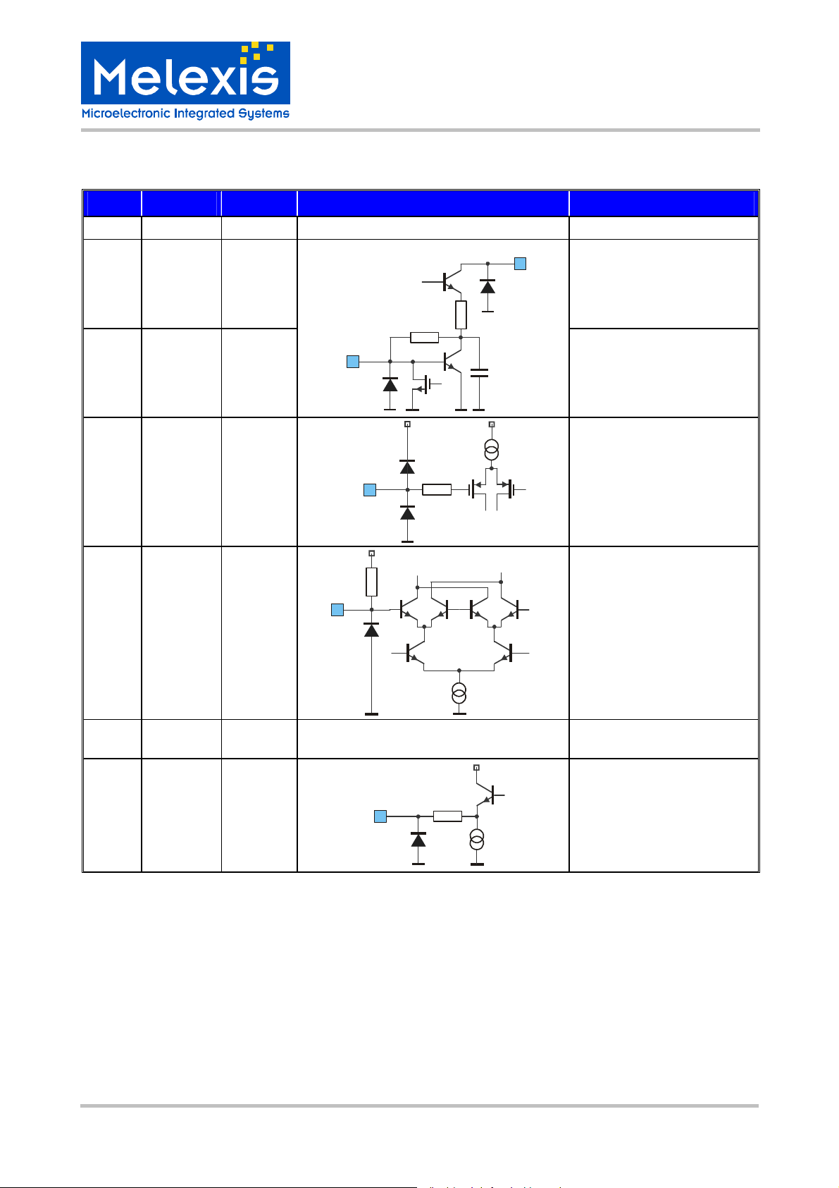
2 Pin Definitions and Descriptions
Pin No. Name I/O Type Functional Schematic Description
1 IN_IFA input
2 VCC_IF supply
3 IN_DEM analog I/O
4 INT2/PDO output
IN_IFA
1
VCC
IN_DEM
3
VEE
INT2/PDO
VCC VCC
2.2k
50
140µA
VEEVEE
VCC
90k
60k
1.5p
10µA
VCC
100µA
VEE
IF amplifier input, approx.
2 kΩ single-ended
positive supply of LNA, MIX,
IFA, FSK Demodulator, PA,
OA1 and OA2
IF amplifier output and demodulator input, connection
to external ceramic discriminator or LC tank
OA2 output or peak detector
output, high impedance in
transmit and idle mode
5 INT1 input
INT1
5
6 OUT_DEM analog I/O
bias
7 RSSI output
OA2
VCC
120
VEE
RSSI
7
4
VEE
200k
VCC
inverting inputs of OA1 and
OA2
+
OA1
VCC
VCC
550k
550k
120
10p
1k
VEE
120
120
10p
31k
OUT_DEM
6
demodulator output and
non-inverting OA1 input,
high impedance in transmit
and idle mode
RSSI output, approx. 31 kΩ
VEE
39010 07122 Page 6 of 44 Data Sheet
Rev. 010 Feb/09
TH7122
27 to 930MHz
FSK/FM/ASK Transceiver
Pin No. Name I/O Type Functional Schematic Description
8 OUT_DTA output
VCC
OUT_DTA
8
OA1 output, high impedance
in transmit and idle mode
9 VEE_RO ground
10 RO analog I/O
11 FSK_SW analog I/O
12 IN_DTA input
13 ASK/FSK input
RO
10
FSK_SW
IN_DTA
12
VEE
ground of RO
2.6µA
36p
39k
VCC
VEE
VCC
36p
RO input, base of bipolar
transistor
FSK pulling pin, switch to
ground or OPEN
The switch is open in re-
11
VEE
VCC
ceive and idle mode
ASK/FSK modulation data
input, pull down resistor
120
120k
VEE
VCC
120kΩ
ASK/FSK mode select input
14 VCC_DIG supply
ASK/FSK
13
VEE
120
positive supply of serial port
and control logic
15 RE/SCLK input
VCC
receiver enable input / clock
input for the shift register,
RE/SCLK
15
16 TE/SDTA input
VCC
120k
VEE
120
pull down resistor 120kΩ
transmitter enable input /
serial data input, pull down
TE/SDTA
16
120k
VEE
120
resistor 120kΩ
39010 07122 Page 7 of 44 Data Sheet
Rev. 010 Feb/09
TH7122
27 to 930MHz
FSK/FM/ASK Transceiver
Pin No. Name I/O Type Functional Schematic Description
17 FS0/SDEN input
FS0/SDEN
17
VCC
120
frequency select input / serial data enable input
18 VEE_DIG ground
19 FS1/LD
input /
output
20 VCC_PLL analog I/O
21 TNK_LO analog I/O
TNK_LO
21
VCC
LF
23
23 LF analog I/O
22 VEE_PLL ground
24 PS_PA analog I/O
VEE
VCC
FS1/LD
19
VEE
6.3pF
VEE
6.5k
VCC
120
VEE
VCC VCC
10µA
120
VD
VCOCUR
VEE
VCC_PLL
20
VEE
ground of serial port and
control logic
frequency select input / lock
detector output
VCO open-collector output,
connection to VCC or external LC tank
VCO open-collector output,
connection to external LC
tank
charge pump output, connection to external loop filter
ground of PLL frequency
synthesizer
power-setting input
PS_PA
24
25 OUT_PA output
OUT_PA
120
VEE VEE
25
20p
VEE VEE
VCC
1k
power amplifier opencollector output
39010 07122 Page 8 of 44 Data Sheet
Rev. 010 Feb/09
TH7122
C
27 to 930MHz
FSK/FM/ASK Transceiver
Pin No. Name I/O Type Functional Schematic Description
27 VEE_LNA ground
28 OUT_LNA output
26 IN_LNA input
OUT_LNA
bias
37
3.8k
IN_LNA
28
VEE
ground of LNA and PA
LNA open-collector output,
connection to external LC
tank at RF
LNA input, single-ended
29 GAIN_LNA input
30 IN_MIX input
31 VEE_IF ground
32 OUT_MIX output
26
GAIN_LNA
IN_MIX
30
29
VEE
VCC
210
LO
VEE VEE
OUT_MIX
120
VC
100
VCC
0.8p
VEEVEE
LNA gain control input
mixer input, approx. 200Ω
single-ended
bias
ground of IFA, Demodulator,
OA1 and OA2
mixer output, approx. 330Ω
single-ended
32
VEE
39010 07122 Page 9 of 44 Data Sheet
Rev. 010 Feb/09
TH7122
27 to 930MHz
FSK/FM/ASK Transceiver
3 Functional Description
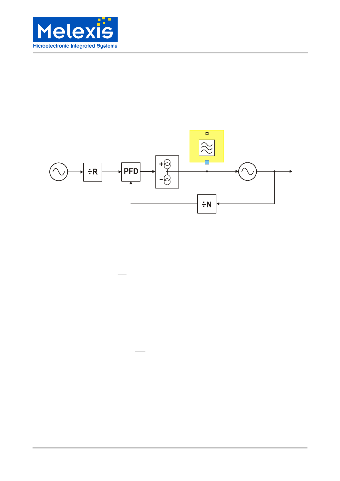
3.1 PLL Frequency Synthesizer
The TH7122 contains an integer-N PLL frequency synthesizer. A PLL circuit performs the frequency synthesis via a feedback mechanism. The output frequency f
detector comparison frequency f
of a crystal oscillator. The phase detector utilizes this signal as a reference to tune the VCO and in the
f
RO
.This reference frequency fR is generated by dividing the output frequency
R
locked state it must be equal to the desired output frequency, divided by the feedback divider ratio N.
Reference
Oscillator
f
RO
Reference
Divider
Phase-frequency
Detector
f
R
Charge
Pump
f
N
Fig. 2: Integer-N PLL Frequency Synthesizer Topology
The output frequency of the synthesizer f
can be selected by programming the feedback divider and the
VCO
reference divider. The only constraint for the frequency output of the system is that the minimum frequency
resolution, or the channel spacing, must be equal to the PFD frequency f
frequency f
and the reference divider factor R:
RO
f
RO
f
R
. (1)
=
R
When the PLL is unlocked (e.g. during power up or during reprogramming of a new feedback divider ratio N),
the phase-frequency detector PFD and the charge pump create an error signal proportional to the phase
difference of the two input signals. This error signal is low-pass filtered through the external loop filter and
input to the VCO to control its frequency. A very low frequency resolution increases the settling time of the
PLL and reduces the ability to cancel out VCO perturbations, because the loop filter is updated every 1/f
After the PLL has locked, the VCO frequency is given by the following equation:
f
VCO
RO
N f ⋅=⋅=
R
fN
There are four registers available to set the VCO frequencies in receive (registers RR and NR) and in transmit mode (registers RT and NT). These registers can be programmed using the Serial Control Interface in
Programmable User Mode (PUM). In case of Stand-alone User Mode (SUM), the registers are set fixed values (refer to para. 4.1.1).
The VCO frequency is equal to the carrier frequency in transmit mode. While in receive mode the VCO
frequency is offset by the intermediate frequency IF. This is because of the super-heterodyne nature of the
receive part.
is generated as an integer multiple of the phase
VCO
VCC
External
Loop Filter
LF
Feedback
Divider
. (2)
R
Voltage Controlled
Oscillator
, which is given by the reference
R
f
VCO
.
R
39010 07122 Page 10 of 44 Data Sheet
Rev. 010 Feb/09
TH7122
⋅
≤
≤
27 to 930MHz
FSK/FM/ASK Transceiver
3.1.1 Reference Oscillator (XOSC)
The reference oscillator is based on a Colpitts topology with two integrated functional capacitors as shown in
figure 3. The circuitry is optimized for a load capacitance range of 10 pF to 15 pF. The equivalent input
capacitance CRO offered by the oscillator input pin RO is about 18pF.
XTAL
CX2
CX1
RO
FSKSW
36pF
VCC
VEE
I
RO
36pF
To ensure a fast and reliable start-up and a very stable frequency
over the specified supply voltage and temperature range, the
oscillator bias circuitry provides an amplitude regulation. The amplitude on pin RO is monitored in order to regulate the current of
the oscillator core I
. There are two limits ROMAX and ROMIN
RO
between the regulation is maintained. These values can be
changed via serial control interface in Programmable User Mode
(PUM). In Stand-alone User Mode (SUM), ROMAX and ROMIN
are set to default values (refer to para. 5.1.3). ROMAX defines the
start-up current of the oscillator. The ROMIN value sets the desired steady-state current. If ROMIN is sufficient to achieve an
amplitude of about 400 mV on pin RO, the current I
will be set
RO
to ROMIN. Otherwise the current will be permanently regulated
between ROMIN and ROMAX. If ROMIN and ROMAX are equal,
no regulation takes place. For most of the applications ROMIN
and ROMAX should not be changed from default.
Fig. 3: Reference oscillator circuit
3.1.2 Reference Divider
The reference divider provides the input signal of the phase detector by dividing the signal of the reference
oscillator. The range of the reference divider is
1023R4 ≤≤ . (3)
3.1.3 Feedback Divider
The feedback divider of the PLL is based on a pulse-swallow topology. It contains a 4-bit swallow A-counter,
a 13-bit program B-counter and a prescaler. The divider ratio of the prescaler is controlled by the program
counter and the swallow counter. During one cycle, the prescaler divides by 17 until the swallow A-counter
reaches its terminal count. Afterwards the prescaler divides by 16 until the program counter reaches its
terminal count. Therefore the overall feedback divider ratio can be expressed as:
+⋅= . (4)
The A-counter configuration represents the lower bits in the feedback divider register (N
upper bits the B-counter configuration (N
4-16
= B
ranges are implemented:
15A0 ≤≤ ; 8191B4
and therefore the range of the overall feedback divider ratio results in:
A)-(B16A17N
= A
) respectively. According to that, the following counter
0-12
0-3
whereas > A (5) B
) and the
0-3
131071N64 ≤≤ . (6)
The user does not need to care about the A- and B-counter settings. It is only necessary to know the overall
feedback divider ratio N to program the register settings.
3.1.4 Frequency Resolution and Operating Frequency
It is obvious from (2) that, at a given frequency resolution fR, the maximum operating frequency of the VCO is
limited by the maximum N-counter setting. The table below provides some illustrative numbers. Please also
refer to section 4.4.1 for the pre-configured settings in Stand-alone User Mode (SUM).
39010 07122 Page 11 of 44 Data Sheet
Rev. 010 Feb/09
TH7122
27 to 930MHz
FSK/FM/ASK Transceiver
Crystal
frequency fRO
3.0000MHz 2.93kHz 1023 13107 38.437MHz
3.0000MHz 2.93kHz 1023 131071 384.372MHz
8.0000MHz 12.5kHz 640 35812 447.65MHz
8.0000MHz 25kHz 320 34746 868.65MHz
8.0000MHz 250kHz 32 3660 915.0MHz
3.1.5 Phase-Frequency Detector
The phase-frequency detector creates an error voltage proportional to the phase difference between the
reference signal f
is very useful because it decreases the acquisition time significantly. The gain of the phase detector can be
expressed as:
where ICP is the charge pump current which is set via register CPCUR. In the TH7122 design the VCO
frequency control characteristic is with negative polarity. This means the VCO frequency increases if the loop
filter output voltage decreases and vice versa. When an external varactor diode is added to the VCO tank,
the tuning characteristic can be changed between positive and negative depending on the particular varactor
diode circuitry. Therefore the PDFPOL register can be used to define the phase detector polarity.
and fN. The implementation of the phase detector is a phase-frequency type. That circuitry
R
Frequency
resolution fR
I
= , (7)
K
PD
CP
R
counter
N
counter
Operating
frequency f
VCO
π2
3.1.6 Lock Detector
In Programmable User Mode a lock-detect signal LD is available at pin FS1/LD (pin 19). The lock detection
circuitry uses Up and Down signals from the phase detector to check them for phase coherency. Figure 4
shows an overview of the lock signal generation. The locked state and the unlock condition will be decided
on the register settings of LDTM and ERTM respectively. In the start-up phase of the PLL, Up and Down
signals are quite unbalanced and counter CNT_LD receives no clock signal. When the loop approaches
steady state, the signals Up and Down begin to overlap and CNT_LD counts down. Herein register LDTM
sets the number of counts which are necessary to set the lock detection signal LD. If an unlock condition
occurs, the counter CNT_LD will be reloaded and therefore its CARRY falls back.
LDTM [1 : 0]
Up
Down
PFD
ERTM [1 : 0]
2
&
&
D
CR
LOAD
CNT_LD
CARRY
=
2
D
CARRY
F
RO
&
RO
CR
LOAD
CNT_ER
Control
Logic
RESET LD
S
LOCKMODE
QR
MUX
Fig. 4: Lock Detection Circuit
LD
39010 07122 Page 12 of 44 Data Sheet
Rev. 010 Feb/09
TH7122
V
27 to 930MHz
FSK/FM/ASK Transceiver
The CNT_ER supervises the unlock condition. If Up and Down are consecutive, the counter CNT_ER will be
reloaded permanently and its CARRY will not be set, otherwise the counter level of CNT_ER will be reduced
by the reference oscillator clock (1/f
during Up and Down signals can be non-consecutive without loosing the locked state.
The transceiver offers two ways of analyzing the locked state. If the register LOCKMODE is set to ‘0’, only
one occurrence of the locked state condition is needed to remain LD = 1 during the whole active mode, otherwise the state of the PLL will be observed permanently.
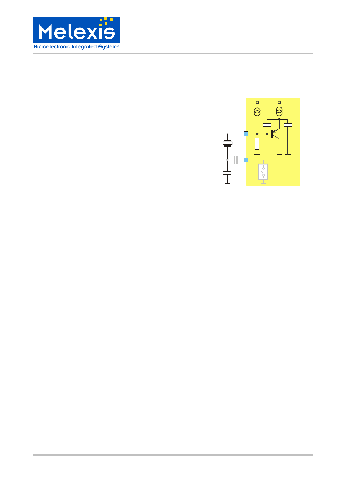
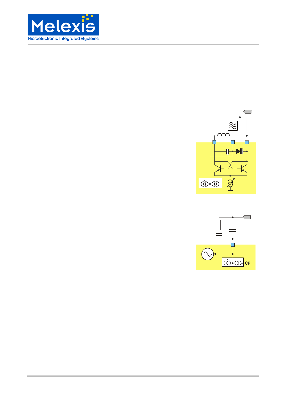
3.1.7 Voltage Controlled Oscillator with external Loop Filter
The transceiver provides a LC-based voltage-controlled oscillator with an
external inductance element connected between VCC and pin TNK_LO.
An internal varactor diode in series with a fixed capacitor forms the variable part of the oscillator tank. The oscillation frequency is adjusted by
the DC-voltage at pin LF. The tuning sensitivity of the VCO is approximately 20MHz/V for 433MHz operations and 40MHz/V at 868MHz. Since
the internal varactor is connected to VCC, a lower voltage on pin LF
causes the capacitance to decrease and the VCO frequency to increase.
For this reason the phase detector polarity should be negative (PFDPOL
= 0). If the operation frequency is below 300MHz, an external varactor
diode between pin TNK_LO and VCC_PLL is necessary. The corresponding application schematic is shown in section 8. The VCO current
VCOCUR can be adjusted via serial control interface in order to ensure
stable oscillations over the whole frequency range. For lowest LO emission in receive mode, VCOCUR should be set to the lowest value.
). The register ERTM decides on the maximum number of clocks
RO
VCC
External
Loop Filter
TNK_LO LF
6.3pF
VCC_PLL
VD
+
Charge Pump
VCOCUR
VEE
Fig. 5: VCO schematic
3.1.8 Loop Filter
Since the loop filter has a strong impact on the function of the PLL, it
must be chosen carefully. For FSK operation the bandwidth of the loop
filter must be selected wide enough for a fast relock of the PLL during
crystal pulling. The bandwidth must of course also be larger than the data
rate. In case of ASK or OOK the bandwidth should be extended even
further to allow the PLL to cancel out VCO perturbations that might be
caused by the PA on/off keying. The suggested filter topology is shown in
Fig. 6. The dimensions of the loop filter elements can be derived using
well known formulas in application notes and other reference literature.
Fig. 6: 2
nd
order Loop filter
RF
CF1
CO
VCC
CF2
LF
+
3.2 Receiver Part
The RF front-end of the receiver part is a super-heterodyne configuration that converts the input radiofrequency (RF) signal into an intermediate frequency (IF) signal. The most commonly used IF is 10.7 MHz,
but IFs in the range of 0.4 to 22 MHz can also be used. According to the block diagram, the front-end consists of a LNA, a Mixer and an IF limiting amplifier with received signal strength indicator (RSSI). The local
oscillator (LO) signal for the mixer is generated by the PLL frequency synthesizer.
As the receiver constitutes a superhet architecture, there is no inherent suppression of the image frequency.
It depends on the particular application and the system’s environmental conditions whether an RF front-end
filter should be added or not. If image rejection and/or good blocking immunity are relevant system parameters, a band-pass filter must be placed either in front or after the LNA. This filter can be a SAW (surface
acoustic wave) or LC-based filter (e.g. helix type).
39010 07122 Page 13 of 44 Data Sheet
Rev. 010 Feb/09

TH7122
27 to 930MHz
FSK/FM/ASK Transceiver
3.2.1 LNA
The LNA is based on a cascode topology for low-noise, high gain and good reverse isolation. The open collector output has to be connected to an external resonance circuit which is tuned to the receive frequency.
The gain of the LNA can be changed in order to achieve a high dynamic range. There are two possibilities for
the gain setting which can be selected by the register bit LNACTRL. External control can be done via the pin
GAIN_LNA, internal control is given by the register bit LNAGAIN. In case of external gain control, a hysteresis of about 340 mV can be chosen via the register bit LNAHYST. This configuration is useful if an automatic
gain control loop via the RSSI signal is established. In transmit mode the LNA-input is shorted to protect the
amplifier from saturation and damaging.
3.2.2 Mixer
The mixer is a double-balanced mixer which down converts the receive frequency to the IF. The default LO
injection type is low side (f
the data signal´s polarity is inverted due to the mixing process. To avoid this, the transmitted data stream can
be inverted too by setting DTAPOL to ‘1’.
The output impedance of the mixer is about 330Ω in order to match to an external IF filter.
= fRX – fIF). But also high side injection is possible (f
VCO
3.2.3 IF Amplifier
After passing the channel select filter which sets the IF bandwidth the signal is limited by means of an high
gain limiting amplifier. The small signal gain is about 80 dB. The RSSI signal is generated within the IF amplifier. The output of the RSSI signal is available at pin RSSI. The voltage at this pin is proportional to the input
power of the receiver in dBm. Using this RSSI output signal the signal strength of different transmitters can
be distinguished.
= fRX + fIF). In this case,
VCO
3.2.4 ASK Demodulator
The receive part of the TH7122 allows for two ASK demodulation configurations:
• standard ASK demodulation or
• ASK demodulation with peak detector.
The default setting is standard ASK demodulation. In this mode SW1 and SW2 are closed and the RSSI
output signal directly feeds the data slicer setup by means of OA1. The data slicer time constant equals to
C3200kT ⋅Ω= , (8)
with C3 external to pin INT1. This time constant should be larger than the longest possible bit duration of the
data stream. This is required to properly extract the ASK data’s DC level. The purpose of the DC (or mean)
level at the negative input of OA1 is to set an adaptive comparator threshold to perform the ASK detection.
Alternatively a peak detector can be used to define the ASK detection threshold. In this configuration the
peak detector PKDET is enabled, SW1 is closed and SW2 is open, and the peak detector output is multiplexed to pin INT2/PDO. This way the peak detector can feed the data slicer, again constituted by OA1 and a
few external R and C components. The peak detection mode is selectable in programmable user mode.
39010 07122 Page 14 of 44 Data Sheet
Rev. 010 Feb/09

TH7122
27 to 930MHz
FSK/FM/ASK Transceiver
3.2.5 FSK Demodulator
The implemented FSK demodulator is based on the phase-coincidence principle. A discriminator tank, which
can either consist of a ceramic discriminator or an LC tank, is connected to pin IN_DEM. If FSK mode is
selected SW1 is open, SW2 is closed and the output of OA2 is multiplexed to pin INT2/PDO.
The demodulator output signal directly feeds the data slicer setup by means of OA1. The data slicer time
constant can be calculated using (8). This time constant should be larger than the longest possible bit duration of the data stream as described in the previous paragraph.
An on-chip AFC circuit tolerates input frequency variations. The input frequency acceptance range is proportional to the FSK or FM deviation. It can be adjusted by the discriminator tank. The AFC feature is disabled
by default and can be activated in programmable mode.
3.3 Transmitter Part
The output of the PLL frequency synthesizer feeds a power amplifier (PA) in order to setup a complete RF
transmitter. The VCO frequency is identical to the carrier frequency.
3.3.1 Power Amplifier
The power amplifier (PA) has been designed to deliver about 10 dBm in the specified frequency bands. Its
pin OUT_PA is an open collector output. The larger the output voltage swing can be made the better the
power efficiency will be. The PA must be matched to deliver the best efficiency in terms of output power and
current consumption.
The collector must be biased to the positive supply. This is
done by means of an inductor parallel tuned with a capacitor. Or it is made large enough in order not to affect the output matching network. S-parameters of pin OUT_PA are not
useful because the output is very high resistive with a small
portion of parallel capacitance. Since the open-collector
output transistor can be considered as a current source, the
only parameters needed to design the output matching network are the output capacitance, the supply voltage V
CC
, the
transistor’s saturation voltage and the power delivered to the
load P
.
O
In order to avoid saturation of the output stage, a saturation
voltage VCE
of about 0.7 V should be considered. The
SAT
real part of the load impedance can then be calculated using
= . (9)
R
L
−
P 2
⋅
O
2
)VCE(V
SATCC
The output capacitance is typically 3 pF.
VCC
3pF
LR
OUT_PA
VEE
Fig. 7: OUT_PA schematic
VCC
L
39010 07122 Page 15 of 44 Data Sheet
Rev. 010 Feb/09

P
m
3.3.2 Output Power Adjustment
The maximum output power is adjustable via
the external resistor RPS as shown in Figure
8. There are four predefined power settings
in programmable user mode which can be
set in the register TXPOWER. The maximum power setting P4 is the default setting.
Fig. 8: Output power vs. RPS
20.
10.
0.00
/ dB
0
-10.00
-20.00
-30.00
-40.00
TH7122
27 to 930MHz
FSK/FM/ASK Transceiver
00
00
P4
101
RPS / kOh m
315MHz
433MHz
868MHz
915MHz
100
3.3.3 Modulation Schemes
The RF carrier generated by the PLL frequency synthesizer can be ASK or FSK modulated. Depending on
the selected user mode, the modulation type can be selected either by the ASK/FSK pin or via the serial
control interface. Data is applied to pin IN_DTA. The data signal can be inverted by the bit DTAPOL. The
following tables for ASK and FSK modulation are valid for non-inverted data (DTAPOL = 0)
3.3.4 ASK Modulation
IN_DTA Description
0 Power amplifier is turned off
1
Power amplifier is turned on
(according to the selected output power)
The transceiver is ASK-modulated by
turning on and off the power amplifier.
Please also refer to para. 1.3 for ASK
modulation limits.
39010 07122 Page 16 of 44 Data Sheet
Rev. 010 Feb/09

TH7122
27 to 930MHz
FSK/FM/ASK Transceiver
3.3.5 FSK Modulation
• FSK modulation via crystal pulling
FSK modulation can be achieved by pulling the crystal oscillator
frequency. A CMOS-compatible data stream applied at pin
IN_DTA digitally modulates the XOSC via an integrated NMOS
switch. Two external pulling capacitors CX1 and CX2 allow the
FSK deviation Δf and center frequency f
to be adjusted inde-
c
pendently. At IN_DTA = LOW CX2 is connected in parallel to CX1
leading to the low-frequency component of the FSK spectrum
); while at IN_DTA = HIGH CX2 is deactivated and the XOSC
(f
min
is set to its high frequency, leading to f
max
.
IN_DTA Description
0
1
= fc - Δf (FSK switch is closed)
f
min
= fc + Δf (FSK switch is open)
f
max
An external reference signal can be directly AC-coupled to the reference oscillator input pin RO. Then the
transceiver is used without a XTAL. Now the reference signal sets the carrier frequency and has to contain
the FSK (or FM) modulation
• FSK modulation via direct VCO modulation
Alternatively FSK or FM can be achieved by injecting the modulating signal into the loop filter to directly control the VCO frequency. Fig. 10 shows a circuit proposal for direct VCO modulation. This circuit is recommended for data rates in excess of about
20 kbps NRZ. An external VCO tuning varactor should be added
for narrow-band applications, for example at channel spacings of
25 kHz. For details please refer to the application notes “TH7122
and TH71221 High Speed Data Communication” and “TH7122
and TH71221 Used In Narrow Band FSK Applications” as well as
to the “TH7122 and TH71221 Cookbook”
VCC
36pF
RO
XTAL
CX2
VEE
FSKSW
CX1
Fig. 9: Crystal Pulling Circuit
IN_DTA
VCC
CM1
RF
CF2
CB6
RM1
L0
CF1
17
18
19
20
21
22
23
24
I
RO
36pF
FS0/SDEN
VEE_DIG
FS1/LD
VCC_PLL
TNK_LO
VEE_PLL
LF
Fig. 10: Circuit schematic for direct VCO modulation
3.3.6 Crystal Tuning
A crystal is tuned by the manufacturer to the requested oscillation frequency f
for a certain load
0
capacitance CL within the specified calibration
tolerance. The only way to tune this oscillation
frequency is to vary the effective load capacitance
seen by the crystal.
CL
eff
Figure 8 shows the oscillation frequency of a crystal in dependency on the effective load capacitance. This capacitance changes in accordance
with the logic level of IN_DTA around the specified
load capacitance. The figure illustrates the relationship between the external pulling capacitors
and the frequency deviation.
Fig. 11: Crystal Tuning Characteristic
39010 07122 Page 17 of 44 Data Sheet
Rev. 010 Feb/09
f
XTAL
f
max
f
o
L1
C1
R1
C0
CL
eff
f
min
CX1+CRO
CLCX1 CRO
(CX1+CX2) CRO
CX1+CX2+CRO
CL
eff

TH7122
27 to 930MHz
FSK/FM/ASK Transceiver
4 Description of User Modes
4.1 Stand-alone User Mode Operation
After power up the transceiver is set to stand-alone user mode. In this mode, pins FS0/SDEN and FS1/LD
must be connected to V
must not be changed after power up in order to remain in stand-alone user mode. The default settings of the
control word bits in stand-alone user mode are described in the frequency selection table. Detailed information about the default settings can be found in the tables of section 5.
4.1.1 Frequency Selection
Channel frequency 433.92 MHz 868.3 MHz 315 MHz 915 MHz
or VCC to set the desired frequency of operation. The logic level at pin FS0/SDEN
EE
FS0/SDEN
FS1/LD
Reference oscillator frequency
R counter ratio in RX mode (RR)
PFD frequency in RX mode
N counter ratio in RX mode (NR)
VCO frequency in RX mode
RX frequency
R counter ratio in TX mode (RT)
PFD frequency in TX mode
N counter ratio in TX mode (NT)
VCO frequency in TX mode
TX frequency
IF in RX mode
In stand-alone user mode, the transceiver can be set to Standby, Receive, Transmit or Idle mode (only PLL
synthesizer active) via control pins RE/SCLK and TE/SDTA. The modulation scheme and the LNA gain are
set by pins ASK/FSK and GAIN_LNA, respectively.
1 0 1 0
0 0 1 1
7.1505 MHz
32 16 18 32
223.45 kHz 446.91 kHz 397.25 kHz 223.45 kHz
1894 1919 766 4047
423.22 MHz 857.60 MHz 304.30 MHz 904.30 MHz
433.92 MHz 868.30 MHz 315.00 MHz 915.00 MHz
32 16 18 32
223.45 kHz 446.91 kHz 397.25 kHz 223.45 kHz
1942 1943 793 4095
433.92 MHz 868.30 MHz 315.00 MHz 915.00 MHz
433.92 MHz 868.30 MHz 315.00 MHz 915.00 MHz
10.7 MHz 10.7 MHz 10.7 MHz 10.7 MHz
4.1.2 Operation Mode
Operation mode Standby Receive Transmit Idle
RE/SCLK
TE/SDTA
Note: Pins with internal pull-down
39010 07122 Page 18 of 44 Data Sheet
Rev. 010 Feb/09
0 1 0 1
0 0 1 1

4.1.3 Modulation Type
Modulation type ASK FSK
TH7122
27 to 930MHz
FSK/FM/ASK Transceiver
ASK / FSK
0 1
4.1.4 LNA Gain Mode
LNA gain high low
GAIN_LNA
0 1
4.2 Programmable User Mode Operation
The transceiver can also be used in programmable user mode. After power-up the first logic change at pin
FS0/SDEN enters into this mode. Now full programmability can be achieved via the Serial Control Interface
(SCI).
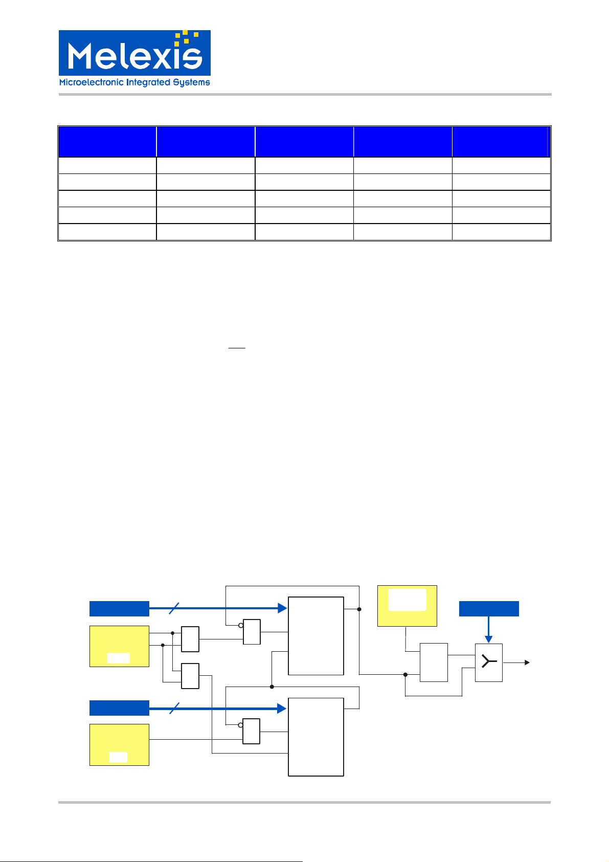
4.2.1 Serial Control Interface Description
A 3-wire (SCLK, SDTA, SDEN) Serial Control Interface (SCI) is used to program the transceiver in programmable user mode. At each rising edge of the SCLK signal, the logic value on the SDTA pin is written into a
24-bit shift register. The data stored in the shift register are loaded into one of the 4 appropriate latches on
the rising edge of SDEN. The control words are 24 bits lengths: 2 address bits and 22 data bits. The first two
bits (bit 23 and 22) are latch address bits. As additional leading bits are ignored, only the least significant 24
bits are serial-clocked into the shift register. The first incoming bit is the most significant bit (MSB). To
program the transceiver in multi-channel application, four 24-bit words may be sent: A-word, B-word, C-word
and D-word. If individual bits within a word have to be changed, then it is sufficient to program only the
appropriate 24-bit word. The serial data input timing and the structure of the control words are illustrated in
Fig. 12 and 13.
SDTA
SCLK
SDEN
24-BIT
SHIFT REGISTER
2
ADDR DECODER
‘’
00
‘’
01
‘’
10
‘’
11
2222
A - LATCH
22
B - LATCH
22
C - LATCH
22
D - LATCH
22
22
22
22
A-word
B-word
C-word
D-word
Fig. 12: SCI Block Diagram
39010 07122 Page 19 of 44 Data Sheet
Rev. 010 Feb/09

TH7122
27 to 930MHz
FSK/FM/ASK Transceiver
Due to the static CMOS design, the SCI consumes virtually no current and it can be programmed in active as
well as in standby mode.
If the transceiver is set from standby mode to any of the active modes (idle, receive, transmit), the SCI settings remain the same as previously set in one of the active modes, unless new settings are done on the SCI
while entering into an active mode.
Invalid
data
SDTA
SCLK
SDEN
MSB
bit 23 bit 22 bit 1 bit 0
t
CS
t
CH
t
CWL
t
CWH
Invalid
dataLSB
t
ES
t
EWtEH
Fig. 13: Serial Data Input Timing
5 Register Description
As shown in the previous section there are four control words which stipulate the operation of the whole chip.
In Stand-alone User Mode SUM the intrinsic default values with respect to the applied levels at pins FS0 and
FS1 lay down the configuration of the transceiver. In Programmable User Mode (PUM) the register settings
can be changed via 3-wire interface SCI. The default settings which vary with the desired operating frequency depend on the voltage levels at the frequency selection pins FS0 and FS1 before entering the PUM.
Table 5.1.1 shows the default register settings of different frequency selections. It should be noted that the
channel frequency listed below will be achieved with a crystal frequency of 7.1505 MHz. The following table
depicts an overview of the register configuration of the TH7122.
39010 07122 Page 20 of 44 Data Sheet
Rev. 010 Feb/09

TH7122
27 to 930MHz
FSK/FM/ASK Transceiver
5.1 Register Overview
WORD
MSB LSB
DATA
23 22 21 20 19 18 17 16 15 14 13 12 11 10 9 8 7 6 5 4 3 2 1 0
0 0 0 0 0 0 0 1 1 1 1 1 0 0
A
23 22 21 20 19 18 17 16 15 14 13 12 11 10 9 8 7 6 5 4 3 2 1 0
0 1 0 1 1 1 0 0 1 1 1 0 1 0
B
23 22 21 20 19 18 17 16 15 14 13 12 11 10 9 8 7 6 5 4 3 2 1 0
1 0 0 0
C
23 22 21 20 19 18 17 16 15 14 13 12 11 10 9 8 7 6 5 4 3 2 1 0
1 1 0 0 1 0 0
IDLE
DATAPOL
PKDET
Set to 1
PFDPOL
LNACTRL
CPCUR
MODSEL
DELPLL
LNAHYST
[ 1 :0 ]
VCOCUR
PACTRL
LOCKMODE
AFC
BAND
TXPOWER
OA2
[ 1 :0 ]
Set to 1
LNAGAIN
[ 2 : 0 ]
ROMAX
Depends on FS0/FS1 voltage level after power up
Depends on FS0/FS1 voltage level after power up
ROMIN
Depends on FS0/FS1 voltage level after power up
[ 1 : 0 ]
OPMODE
Depends on FS0/FS1 voltage level after power up
[ 2 : 0 ]
NR
[ 16 : 0 ]
RR
[ 9 : 0 ]
RT
[ 9 : 0 ]
Bit No.
default
Bit No.
default
Bit No.
default
Bit No.
default
D
LDTM
MODCTRL
[ 1 :0 ]
ERTM
[ 1 :0 ]
NT
[ 16 : 0 ]
5.1.1 Default Register Settings for FS0, FS1
FS1 FS0
0 0
0 1
1 0
1 1
Channel
frequency
868.30 MHz
433.92 MHz
915.00 MHz
315.00 MHz
Note: d – decimal code
A detailed description of the registers function and their configuration can be found in the following sections.
39010 07122 Page 21 of 44 Data Sheet
Rev. 010 Feb/09
BAND VCOCUR
[ 1 : 0 ]
RR
[ 9 : 0 ]
NR
[ 16 :0 ]
RT
[ 9 :0 ]
NT
[ 16 : 0 ]
1 11 16d 1919d 16d 1943d
0 01 32d 1894d 32d 1942d
1 11 32d 4047d 32d 4095d
0 00 18d 766d 18d 793d

5.1.2 A – word
Name Bits Description
TH7122
27 to 930MHz
FSK/FM/ASK Transceiver
RR
OPMODE
LNAGAIN
not used
TXPOWER
PACTRL
LOCKMODE
CPCUR
MODSEL
DTAPOL
IDLESEL
[9:0]
Reference divider ratio in RX operation mode
4d .. 1023d
Operation mode
00
[11:10]
Standby mode
01
Receive mode
10
Transmit mode
11
Idle mode
LNA gain
[12]
0 1 low LNA gain
high LNA gain
This selection is valid if bit LNACTR (bit 21 in C-word) is set to internal LNA gain control.
[13] set to ‘1’ for correct function
Output power steps
00
[15:14]
01
10
11
P1
P2
P3
P4
Set the PA-on condition
[16]
0 1 PA is switched on if the PLL locks
PA is always on in TX mode
Set the PLL locked state observation mode
0 before lock only
[17]
Locked state condition will be ascertained only one time afterwards the LD signal remains in
high state.
1 before and after lock
locked state will be observed permanently
Charge Pump output current
[18]
0 1 260 µA
1300 µA
Modulation mode
0 1 ASK
[19]
FSK
This selection is valid if bit MODCTRL (bit 21 in D-word) is set to internal modulation
control.
Input data polarity
0 normal
[20]
‘0’ for space at ASK or f
at FSK, ‘1’ for mark at ASK or f
min
1 inverse
‘1’ for space at ASK or f
at FSK, ‘0’ for mark at ASK or f
min
Active blocks in IDLE mode
[21]
0 1 only RO active
whole PLL active
at FSK
max
at FSK
max
#default
#default
#default
#default
#default
#default
#default
#default
#default
39010 07122 Page 22 of 44 Data Sheet
Rev. 010 Feb/09

5.1.3 B – word
Name Bits Description
TH7122
27 to 930MHz
FSK/FM/ASK Transceiver
RT
ROMIN
ROMAX
OA2
AFC
LNAHYST
DELPLL
not used
[9:0]
Reference divider ratio in TX operation mode
4d .. 1023d
Set the desired steady state current of the reference oscillator
0 μA
#default
The control circuitry regulates the current of the oscillator core
between the values ROMAX and ROMIN. As the regulation input
signal the amplitude on pin RO is used. If the ROMIN value is
sufficient to achieve an amplitude of about 400mV on pin RO the
current of the reference oscillator core will be set to ROMIN.
Otherwise the current will be permanently regulated between
ROMAX and ROMIN. If ROMIN and ROMAX are equal no
regulation of the oscillator current occurs. Please also note the
block description of the reference oscillator in para. 3.1.1
[12:10]
000
001
010
011
100
101
110
111
75 μA
150 μA
225 μA
300 μA
375 μA
450 μA
525 μA
Set the start-up current of the reference oscillator
0 μA
75 μA
150 μA
225 μA
300 μA
375 μA
450 μA
525 μA
#default
Set the start-up current of the reference oscillator core. Please
also note the description of the ROMIN register and the block
description of the reference oscillator which can be seen above.
[15:13]
000
001
010
011
100
101
110
111
OA2 operation
[16]
0 1 disabled
enabled
OA2 can be enabled in FSK receive mode. OA2 is disabled in ASK mode receive.
Internal AFC feature
[17]
0 1 disabled
enabled
Hysteresis on pin GAIN_LNA
[18]
0 1 disabled
enabled
Delayed start of the PLL
0 undelayed start
PLL starts at the reference oscillator start-up
[19]
1
starts after 8 valid RO-cycles
PLL starts after 8 valid RO-cycles before entering an active mode to ensure reliable oscillation
of the reference oscillator.
[20] set to ‘1’ for correct function
#default
#default
#default
#default
RSSI Peak Detector
#default
PKDET
[21]
0 disabled
The RSSI output signal directly feeds the data slicer setup by means of OA1.
enabled
1
In ASK receive mode the RSSI Peak Detector output is multiplexed to pin INT2/PDO.
39010 07122 Page 23 of 44 Data Sheet
Rev. 010 Feb/09

5.1.4 C – word
Name Bits Description
TH7122
27 to 930MHz
FSK/FM/ASK Transceiver
NR
BAND
VCOCUR
PFDPOL
LNACTRL
[16:0]
[17]
[19:18]
[20]
[21]
Feedback divider ratio in RX operation mode
64d .. 131071d
Set the desired frequency range
0 1 recommended at fRF < 500 MHz
recommended at fRF > 500MHz
Some tail current sources are linked to this bit in order to save current for low frequency
operations.
VCO active current
00
low current (300 µA)
01
standard current (500 µA)
10
high1 current (700 µA)
11
high2 current (900 µA)
Phase Detector polarity
negative
0
1
#default
positive
VCO
OUTPUT
FREQUENCY
pos
neg
VCO INPUT VOLTAGE
LNA gain control mode
0 external LNA gain control
LNA gain will be set via pin GAIN_LNA.
1 internal LNA gain control
LNA gain will be set via bit LNAGAIN (bit 12 in A-word). Nevertheless pin GAIN_LNA must
be connected to either VCC or VEE.
#default
39010 07122 Page 24 of 44 Data Sheet
Rev. 010 Feb/09

5.1.5 D – word
Name Bits Description
TH7122
27 to 930MHz
FSK/FM/ASK Transceiver
NT
ERTM
LDTM
MODCTRL
[16:0]
[18:17]
[20:19]
[21]
Feedback divider ratio in TX operation mode
64d .. 131071d
Set the unlock condition of the PLL
00
01
10
11
00
01
10
11
0 external modulation control
1 internal modulation control
2 clocks
4 clocks
8 clocks
16 clocks
4 clocks
16 clocks
64 clocks
256 clocks
Modulation will be set via pin ASK/FSK.
Modulation will be set via bit MODSEL (bit 19 in A-word). Nevertheless pin ASK/FSK must be
connected to either VCC or VEE.
#default
Set the lock condition of the PLL
#default
Set mode of modulation control:
Set the maximum allowed number of reference clocks
(1/fRO) during the phase detector output signals (UP &
DOWN) can be in-consecutive.
Set the minimum number of consecutive edges of phase
detector output cycles, without appearance of any unlock
condition.
#default
39010 07122 Page 25 of 44 Data Sheet
Rev. 010 Feb/09

TH7122
27 to 930MHz
FSK/FM/ASK Transceiver
6 Technical Data
6.1 Absolute Maximum Ratings
Operation beyond absolute maximum ratings may cause permanent damage of the device.
Parameter Symbol Condition / Note Min Max Unit
Supply voltage VCC -0.3 6.0 V
Input voltage VIN -0.3 Vcc+0.3 V
Input RF level P
Storage temperature T
Junction temperature TJ +150 °C
Power dissipation P
Thermal Resistance R
Electrostatic discharge V
Electrostatic discharge V
1) all pins, except LF, TNK_LO, VCC_PLL and FS1/LD
2) pins LF, TNK_LO, VCC_PLL and FS1/LD
@ LNA input 10 dBm
iRF
-40 +125 °C
STG
0.25 W
diss
60 K/W
thJA
human body model, 1) -1.0 +1.0 kV
ESD1
human body model, 2) -0.75 +0.75 kV
ESD2
6.2 Normal Operating Conditions
Parameter Symbol Condition Min Max Unit
Supply voltage VCC 2.2 5.5 V
Operating temperature TA -40 +85 ºC
Input low voltage (CMOS)
pins IN_DTA, ASK/FSK,
RE/SCLK, TE/SDTA, FS0/SDEN,
V
IL
V
IL_FS1/LD
in Stand-alone user
mode
FS1/LD
Input high voltage (CMOS)
pins IN_DTA, ASK/FSK,
RE/SCLK, TE/SDTA, FS0/SDEN,
V
IH
V
IH_FS1/LD
in Stand-alone user
mode
FS1/LD
Transmit frequency range fTX 300 930 MHz
Receive frequency range fRX 300 930 MHz
VCO frequency f
Set by tank configuration 300 930 MHz
VCO
IF range fIF | fRX - f
FSK
demodulator operating range
f
2 22 MHz
IF_FSK
RO frequency fRO Set by crystal 3 12 MHz
PFD comparison frequency fR
Frequency deviation
Δf
FSK data rate R
ASK data rate R
FSK
ASK
Set by crystal and
R-counter
at FM or FSK
w/ crystal pulling, NRZ 20 kbps
w/ direct VCO mod., NRZ 115 kbps
NRZ 40 kbps
FM bandwidth fm 10 kHz
VCO gain
fRF= 433.92MHz 14 23
= 868.3MHz
f
RF
K
VCO
only
0.3*V
CC
V
only
0.7*V
CC
| 0.4 22 MHz
VCO
V
0.003 1 MHz
±2.5 ±80
28 55
kHz
MHz/V
39010 07122 Page 26 of 44 Data Sheet
Rev. 010 Feb/09

FSK/FM/ASK Transceiver
6.3 DC Characteristics
all parameters under normal operating conditions, unless otherwise stated;
typical values at T
Parameter Symbol Condition Min Typ Max Unit
Operating currents
= 23 °C and VCC = 3 V
A
TH7122
27 to 930MHz
Standby current I
Standby mode 50 200 nA
SBY
Reg. BAND
Idle mode (RO only),
Reg. IDLESEL = 0
Idle mode,
Idle current
I
1 (> 500 MHz) 3.5 4.8
IDLE
(whole PLL),
Receive supply
current - ASK
Receive supply
current - FSK
1 (> 500 MHz)
0 (< 500 MHz) 6.1 8.0
1 (> 500 MHz)
0 (< 500 MHz) 7.4 9.9
1 (> 500 MHz)
0 (< 500 MHz) 6.7 9.0
1 (> 500 MHz)
0 (< 500 MHz) 8.0 10.9
1 (> 500 MHz)
I
RXL_ASK
I
RXH_ASK
I
RXL_FSK
I
RXH_FSK
Reg. IDLESEL = 1
ASK Receive mode,
LNA @ low gain
ASK Receive mode,
LNA @ high gain
FSK Receive mode,
LNA @ low gain
FSK Receive mode,
LNA @ high gain
Transmit mode,
Transmit
supply current
@ P1
0 (< 500 MHz) 13.2 16.2
I
P1
1 (> 500 MHz)
Reg. TXPOWER =00,
V
PS_PA
continuous wave
(CW) mode
Transmit
supply current
@ P2
Transmit
supply current
@ P3
Transmit
supply current
@ P4
0 (< 500 MHz) 15.2 19.2
I
P2
1 (> 500 MHz)
0 (< 500 MHz) 18.6 23.4
I
P3
1 (> 500 MHz)
0 (< 500 MHz) 23.0 30.6
I
P4
1 (> 500 MHz)
Transmit mode,
Reg. TXPOWER =01,
V
PS_PA
CW mode
Transmit mode,
Reg. TXPOWER =10,
V
PS_PA
CW mode
Transmit mode,
Reg. TXPOWER =11,
V
PS_PA
CW mode
Digital pin characteristics
Input low voltage (CMOS)
pins IN_DTA, ASK/FSK,
RE/SCLK, TE/SDTA, FS0/SDEN,
V
IL
V
IL_FS1/LD
in Stand-alone user
mode
FS1/LD
Input high voltage (CMOS)
pins IN_DTA, ASK/FSK,
RE/SCLK, TE/SDTA, FS0/SDEN,
V
IH
V
IH_FS1/LD
in Stand-alone user
mode
FS1/LD
= 0.3V,
= 0.3V,
= 0.3V,
= 0.3V,
only
only
0.3 0.7 mA
mA
6.3 7.8
8.9 12.8
10.2 14.7
9.5 13.6
10.8 15.5
mA
mA
mA
mA
mA
17.1 20.6
mA
19.1 23.9
mA
22.5 28.6
mA
26.9 36.7
-0.3
0.7*V
CC
0.3*VCC V
Vcc+0.3 V
39010 07122 Page 27 of 44 Data Sheet
Rev. 010 Feb/09

TH7122
27 to 930MHz
FSK/FM/ASK Transceiver
Parameter Symbol Condition Min Typ Max Unit
Digital pin characteristics
Pull-down Resistor
R
pins IN_DTA , RE/SCLK,
70 120 220
PD
TE/SDTA
Low level input leakage current
pins IN_DTA, ASK/FSK,
RE/SCLK, TE/SDTA, FS0/SDEN,
I
INL_FS1/LD
I
IL
in Stand-alone user
mode
only
-2
FS1/LD
High level input leakage current
pins ASK/FSK, FS0/SDEN,
FS1/LD
I
INH_FS1/LD
I
IH
in Stand-alone user
mode
only
2
Analog pin characteristics
MOS switch On resistance
FSK_SW pin
R
ON
Transmit mode,
if Reg. DTAPOL = 0:
IN_DTA = 0
10 30
if Reg. DTAPOL = 1:
IN_DTA = 1
MOS switch Off resistance
FSK_SW pin
R
OFF
Transmit mode,
if Reg. DTAPOL = 0:
IN_DTA = 1
1
if Reg. DTAPOL = 1:
IN_DTA = 0
Peak detector pull-up current
INT2/PDO pin I
Peak detector leakage current
INT2/PDO pin
PU_PDO
I
L_PDO
ASK Receive mode,
Reg. PKDET = 1
V
OUT_DEM
ASK Receive mode,
Reg. PKDET = 1
V
OUT_DEM
> V
=< V
INT2/PDO
INT2/PDO
-1.1 mA
-2 2
OA input offset voltage VOS Receive mode -25 25 mV
Voltage threshold for high to low
LNA gain transition
GAIN_LNA pin
Voltage threshold for low to high
LNA gain transition
GAIN_LNA pin
V
GAIN_HL
V
GAIN_LH
Receive mode,
Reg. LNACTRL = 0,
Reg. LNAHYST = 1
Receive mode,
Reg. LNACTRL = 0,
Reg. LNAHYST = 1
1.0 1.3 1.6 V
1.3 1.6 1.9 V
RSSI characteristics
RSSI voltage at low IFA
input level
V
L_RSSI
Receive mode,
V
IN_IFA
= 100μV
0.72 V
(CW, 10.7MHz)
RSSI voltage at high IFA
input level
V
H_RSSI
Receive mode,
V
IN_IFA
= 100mV
1.64 V
(CW, 10.7MHz)
kΩ
μA
μA
Ω
MΩ
μA
39010 07122 Page 28 of 44 Data Sheet
Rev. 010 Feb/09

TH7122
27 to 930MHz
FSK/FM/ASK Transceiver
6.4 PLL Synthesizer Timings
Parameter Symbol Condition Min Typ Max Unit
B
= 20kHz,
Channel
switching time
wide band t
narrow band t
TX – RX switching time
SW_WB
SW_NB
t
TX_RX
PLL
= 260µA
I
CP
B
= 2kHz,
PLL
ICP = 260µA
IF = 10.7MHz 1 ms
6.5 AC Characteristics of the Receiver Part
all parameters under normal operating conditions, unless otherwise stated;
typical values at T
all parameters based on test circuits for FSK (Fig. 14 to 15) and ASK (Fig. 16 to 17), respectively;
Input sensitivity
ASK
Input sensitivity
FSK
Maximum input
signal
ASK
= 23 °C and VCC = 3 V;
a
Parameter Symbol Condition Min Typ Max Unit
= 180kHz, fm = 2kHz
B
fRF= 433.92MHz -96
P
minL_ASK
fRF= 868.3MHz
fRF= 433.92MHz -107
P
minH_ASK
fRF= 868.3MHz
fRF= 433.92MHz -87
P
minL_FSK
fRF= 868.3MHz
fRF= 433.92MHz -105
P
minH_FSK
fRF= 868.3MHz
IF
BER ≤ 3⋅10
-3
LNA @ low gain
BIF = 180kHz, fm = 2kHz
BER ≤ 3⋅10
-3
LNA @ high gain
= 180kHz, fm = 2kHz
B
IF
Δf = ± 50 kHz
BER ≤ 3⋅10
-3
LNA @ low gain
BIF = 180kHz, fm = 2kHz
Δf = ± 50 kHz
BER ≤ 3⋅10
-3
LNA @ high gain
fRF= 433.92MHz -10
P
maxL_ASK
LNA @ low gain
fRF= 868.3MHz
fRF= 433.92MHz -20
P
maxH_ASK
LNA @ high gain
fRF= 868.3MHz
200 µs
500 µs
-96
-107
-87
-105
-10
-20
dBm
dBm
dBm
dBm
dBm
dBm
fRF= 433.92MHz -10
Maximum input
fRF= 868.3MHz
P
maxL_FSK
LNA @ low gain
dBm
-10
signal
FSK
Start-up time - ASK t
Start-up time - FSK t
Spurious emission P
fRF= 433.92MHz -20
fRF= 868.3MHz
P
maxH_FSK
on_ASK
on_FSK
spur_RX
LNA @ high gain
from standby to receive
mode
from standby to receive
mode
referred to receiver
input
-20
1 1.5 ms
1 1.5 ms
-54 dBm
dBm
39010 07122 Page 29 of 44 Data Sheet
Rev. 010 Feb/09

TH7122
27 to 930MHz
FSK/FM/ASK Transceiver
6.6 AC Characteristics of the Transmitter Part
all parameters under normal operating conditions, unless otherwise stated;
typical values at T
all parameters based on test circuits for FSK (Fig. 14 to 15) and ASK (Fig. 16 to 17), respectively;
= 23 °C and VCC = 3 V;
a
Parameter Symbol Condition Min Typ Max
Output power
Output power
Output power
Output power
fRF= 433.92MHz -7
= 868.3MHz
f
RF
fRF= 433.92MHz 1
= 868.3MHz
f
RF
fRF= 433.92MHz 6
= 868.3MHz
f
RF
fRF= 433.92MHz 10
= 868.3MHz
f
RF
FSK deviation
FM deviation
Modulation frequency FM f
PLL reference spurious emission P
Harmonic emission P
Start-up time t
Unit
mode = transmit,
P1
RPS = see para. 7.3
TXPOWER = 00
-10
dBm
mode = transmit,
P2
RPS = see para. 7.3
TXPOWER = 01
-2
dBm
mode = transmit,
P3
RPS = see para. 7.3
TXPOWER = 10
3
dBm
mode = transmit,
P4
RPS = see para. 7.3
TXPOWER = 11
FSK
Δf
FM
10 kHz
mod
spur_PLL
harm
on_TX
and crystal parameters
please refer to the FM
circuit in the cookbook
-40 dBm
-36 dBm
From standby to
transmit mode
depends on C
Δf
, Cx2
x1
9
±2.5 ±25 ±80
±6
dBm
kHz
kHz
1 1.5 ms
6.7 Serial Control Interface
Parameter Symbol Condition Min Max Unit
SDTA to SCLK set up time tCS 150 ns
SCLK to SDTA hold time tCH 50 ns
SCLK pulse width low t
SCLK pulse width high t
100 ns
CWL
100 ns
CWH
SCLK to SDEN set up time tES 100 ns
SDEN pulse width tEW 100 ns
t
SDEN to SCLK hold time
EH
100 ns
6.8 Crystal Parameters
Parameter Symbol Condition Min Max Unit
Crystal frequency f
Load capacitance C
Static capacitance C0 5 pF
Equivalent series resistance R1 180
Spurious response
fundamental mode, AT 3 12 MHz
crystal
10 15 pF
load
a
spur
only required for FSK -10 dB
Ω
39010 07122 Page 30 of 44 Data Sheet
Rev. 010 Feb/09

TH7122
27 to 930MHz
FSK/FM/ASK Transceiver
7 Application Circuit Examples
7.1 FSK Application Circuit Programmable User Mode (internal AFC option)
RX_IN
TX_OUT
Combining
network
L1
CB1
CB2
LTX0
CTX0
CRX0
C2
C1
CTX4
25
26
27
28
29
30
31
32
CF2
CB5
CF1
RF
C0
C3
L0
CB6
C4
Lock
detect
C5
SDEN
SDTA
SCLK
CB7
RSSI
3wire bus
FSK
input
FSK
output
CB0
CB4
RP
CERDIS
VCC
39010 07122 Page 31 of 44 Data Sheet
Rev. 010 Feb/09

A
7.2 FSK Application Circuit Stand-alone User Mode
TH7122
27 to 930MHz
FSK/FM/ASK Transceiver
RX_IN
TX_OUT
Combining
network
L1
CB1
RB1
CB2
LTX0
CTX0
CRX0
C2
C1
RPS
CTX4
25
OUT_PA
IN_LNA
26
VEE_LNA
27
OUT_LNA
28
29
GAIN_LNA
30
IN_MIX
31
VEE_IF
OUT_MIX
32
CERFIL
CF2
CB5
24
IN_IFA
CPS
23
LF
VCC_IF
CF1
RF
CB6
C0
L0
21
22
20
TNK_LO
VEE_PLL
VCC_PLL
TH7122
IN_DEM
INT2/PDO
INT1
C3
C3
see para. 4.1.1
17
18
19
FS0/SDEN
FS1/LD
VEE_DIG
RE/SCLK
VCC_DIG
SK/FSK
IN_DTA
FSK_SW
RO
OUT_DEM
RSSI
OUT_DTA
81234567
C4
C5
16
15
14
13
12
11
10
9
VEE_RO
RSSI
CB7
LX
TX
enable
XTAL
RX
enable
FSK
input
CX2
FSK
output
CX1
CB0
CB4
RP
VCC
CERDIS
Fig. 15: Test circuit for FSK operation in Stand-alone User Mode
39010 07122 Page 32 of 44 Data Sheet
Rev. 010 Feb/09

FSK/FM/ASK Transceiver
7.3 FSK Test Circuit Component List (Fig. 14 and Fig. 15)
Part Size
C0 0603 1.2 pF 1.5 pF 1.8 pF 0.82 pF
C1 0603 3.9 pF 5.6 pF 2.2 pF 1.8 pF
C2 0603 1.5 pF 1.5 pF 1.5 pF 1.5 pF
C3 0603 10 nF 10 nF 10 nF 10 nF
C4 0603 330 pF 330 pF 330 pF 330 pF
C5 0603 1.5 nF 1.5 nF 1.5 nF 1.5 nF
CB0 1210 10 μF 10 μF 10 μF 10 μF
CB1 0603 10 nF 10 nF 10 nF 10 nF
CB2 0603 330 pF 330 pF 330 pF 330 pF
CB4 0603 10 nF 10 nF 10 nF 10 nF
CB5 0603 100 nF 100 nF 100 nF 100 nF
CB6 0603 100 pF 100 pF 100 pF 100 pF
CB7 0603 100 nF 100 nF 100 nF 100 nF
CF1 0603 1 nF 1 nF 1 nF 1 nF
CF2 0603 68 pF 120 pF 150 pF 82 pF
CPS 0603 10 nF 10 nF 10 nF 10 nF
CX1 0603 8.2 pF 10 pF 12 pF 12 pF
CX2 0603 150 pF 56 pF 18 pF 15 pF
CRX0 0603 100 pF 100 pF 100 pF 100 pF
CTX0 0603 10 pF 10 pF 10 pF 10 pF
CTX4 0603 12 pF 4.7 pF 2.2 pF 1.8 pF
RB1 0603
RF 0603
RP 0603
RPS 0603
L0 0603 47 nH 22 nH 3.9 nH 3.9 nH
L1 0603 33 nH 15 nH 4.7 nH 4.7 nH
LTX0 0603 15 nH 15 nH 3.9 nH 3.9 nH
LX 0603
XTAL
CERFIL
CERDIS
HC49
SMD
7x5
SMD
3.45x3.1
SMD
4.5x2
Value @
315 MHz
100 Ω 100 Ω 100 Ω 100 Ω ±5%
47 kΩ 47 kΩ 33 kΩ 33 kΩ ±5%
3.3 kΩ 3.3 kΩ 3.3 kΩ 3.3 kΩ ±5%
22 kΩ 33 kΩ 47 kΩ 47 kΩ ±5%
0 Ω 0 Ω
Note: - Antenna matching network according to paragraph 9
Value @
433.92 MHz
±20ppm cal., ±20ppm temp.
SFECF10M7HA00
CDSCB10M7GA136
Value @
868.3 MHz
7.1505 MHz
= 180 kHz
B
3dB
Value @
915 MHz
10 nH 10 nH
Tol. Description
±5%
±5%
±5%
±10%
±5%
±10%
±20%
±10%
±10%
±10%
±10%
±10%
±10%
±10%
±5%
±10%
±5% RO capacitor for FSK (Δf = ±20 kHz)
±5% RO capacitor for FSK (Δf = ±20 kHz)
±5%
±5%
±5%
±5%
±5%
±5%
±5%
TH7122
27 to 930MHz
VCO tank capacitor
LNA output tank capacitor
MIX input matching capacitor
data slicer capacitor
demodulator output low-pass
capacitor, depending on data rate
RSSI output low pass capacitor
de-coupling capacitor
de-coupling capacitor
de-coupling capacitor
de-coupling capacitor
de-coupling capacitor
de-coupling capacitor
de-coupling capacitor
loop filter capacitor
loop filter capacitor
power-select capacitor
RX coupling capacitor
TX coupling capacitor
TX impedance matching capacitor
protection resistor
loop filter resistor
CERDIS loading resistor
power-select resistor
VCO tank inductor
from Würth-Elektronik (WE-KI series)
or equivalent part
LNA output tank inductor
from Würth-Elektronik (WE-KI series)
or equivalent part
impedance matching inductor
from Würth-Elektronik (WE-KI series)
or equivalent part
RO inductor
fundamental-mode crystal,
= 10 pF to 15pF, C
C
load
R
= 70 Ω
m, max
ceramic filter from Murata,
or equivalent part
ceramic Discriminator from Murata,
or equivalent part
0, max
= 7 pF,
39010 07122 Page 33 of 44 Data Sheet
Rev. 010 Feb/09

TH7122
A
27 to 930MHz
FSK/FM/ASK Transceiver
7.4 ASK Application Circuit Programmable User Mode (normal data slicer option)
RX_IN
TX_OUT
Combining
network
L1
CB1
RB1
CB2
LTX0
CTX0
CRX0
C2
C1
RPS
CTX4
25
OUT_PA
26
IN_LNA
27
VEE_LNA
28
OUT_LNA
29
GAIN_LNA
30
IN_MIX
31
VEE_IF
OUT_MIX
32
CERFIL
CF2
CB5
24
IN_IFA
CPS
23
LF
VCC_IF
CF1
RF
CB6
C0
L0
21
22
VEE_PLL
20
TNK_LO
VCC_PLL
TH7122
IN_DEM
INT2/PDO
INT1
C3
Lock
detect
17
18
19
FS0/SDEN
FS1/LD
VEE_DIG
RE/SCLK
VCC_DIG
SK/FSK
IN_DTA
FSK_SW
OUT_DEM
RSSI
7
8123456
C5
SDEN
SDTA
16
SCLK
15
CB7
14
13
12
11
10
RO
9
VEE_RO
OUT_DTA
RSSI
XTAL
3wire bus
ASK
input
CX1
ASK
output
CB0
VCC
Fig. 16: Test circuit for ASK operation in Programmable User Mode (normal data slicer option)
Software Settings for ASK
Channel
frequency
315.00 MHz
434.00 MHz
915.00 MHz
RR NR RT NT RX TX RX TX
80 3043 8 315 260µA 1300µA 300 µA 900µA
80 4233 8 434 260µA 1300µA 300 µA 900µA
80 9043 8 915 260µA 1300µA 300 µA 900µA
39010 07122 Page 34 of 44 Data Sheet
Rev. 010 Feb/09
fRO = 8.0000MHz CPCUR VCOCUR

7.5 ASK Test Circuit Component List (Fig. 16)
Part Size
C0 0603 1.5 pF 1.8 pF 1 pF
C1 0603 3.9 pF 5.6 pF 1.8 pF
C2 0603 1.5 pF 1.0 pF 1.5 pF
C3 0603 10 nF 10 nF 10 nF
C5 0603 1.5 nF 1.5 nF 1.5 nF
CB0 1210 10 μF 10 μF 10 μF
CB1 0603 10 nF 10 nF 10 nF
CB2 0603 330 pF 330 pF 330 pF
CB5 0603 100 nF 100 nF 100 nF
CB6 0603 100 pF 100 pF 100 pF
CB7 0603 100 nF 100 nF 100 nF
CF1 0603 100 pF 100 pF 100 pF
CF2 0603 39 pF 39 pF 39 pF
CPS 0603 1 nF 1 nF 1 nF
CX1 0805 18 pF 18 pF 18 pF
CRX0 0603 100 pF 100 pF 10 pF
CTX0 0603 10 pF 10 pF 10 pF
CTX4 0603 12 pF 4.7 pF 1.8 pF
RB1 0603
RF 0603
RPS 0603
L0 0603 47 nH 22 nH 3.9 nH
L1 0603 33 nH 15 nH 4.7 nH
LTX0 0603 15 nH 15 nH 3.9 nH
XTAL
CERFIL
HC49
SMD
7x5
SMD
3.45x3.1
Value @
315 MHz
100 Ω 100 Ω 100 Ω ±5%
33 kΩ 33 kΩ 33 kΩ ±5%
18 kΩ 33 kΩ 43 kΩ ±5%
Note: - Antenna matching network according to paragraph 9
Value @
434 MHz
8.0000 MHz
±20ppm cal., ±20ppm temp.
SFECF10M7HA00
= 180 kHz
B
3dB
Value @
915 MHz
TH7122
27 to 930MHz
FSK/FM/ASK Transceiver
Tol. Description
±5%
±5%
±5%
±10%
±10%
±20%
±10%
±10%
±10%
±10%
±10%
±10%
±5%
±10%
±5%
±5%
±5%
±5%
±5%
±5%
±5%
VCO tank capacitor
LNA output tank capacitor
MIX input matching capacitor
data slicer capacitor
RSSI output low pass capacitor
de-coupling capacitor
de-coupling capacitor
de-coupling capacitor
de-coupling capacitor
de-coupling capacitor
de-coupling capacitor
loop filter capacitor
loop filter capacitor
power-select capacitor,
depending on data rate
RO capacitor
RX coupling capacitor
TX coupling capacitor
TX impedance matching capacitor
protection resistor
loop filter resistor
power-select resistor
VCO tank inductor
from Würth-Elektronik (WE-KI series)
or equivalent part
LNA output tank inductor
from Würth-Elektronik (WE-KI series)
or equivalent part
impedance matching inductor
from Würth-Elektronik (WE-KI series)
or equivalent part
fundamental-mode crystal,
= 10 pF to 15pF, C
C
load
= 70 Ω
R
m, max
ceramic filter from Murata,
or equivalent part
0, max
= 7 pF,
39010 07122 Page 35 of 44 Data Sheet
Rev. 010 Feb/09

TH7122
A
27 to 930MHz
FSK/FM/ASK Transceiver
7.6 ASK Application Circuit Programmable User Mode (peak detector option)
RX_IN
TX_OUT
Combining
network
L1
CB1
RB1
CB2
LTX0
CTX0
CRX0
C2
C1
RPS
CTX4
25
OUT_PA
26
IN_LNA
27
VEE_LNA
28
OUT_LNA
29
GAIN_LNA
30
IN_MIX
31
VEE_IF
OUT_MIX
32
CERFIL
CF2
CB5
24
IN_IFA
CPS
23
LF
VCC_IF
C6
CF1
RF
CB6
C0
L0
21
22
VEE_PLL
20
TNK_LO
VCC_PLL
TH7122
IN_DEM
INT2/PDO
INT1
R2R1
Lock
detect
17
18
19
FS0/SDEN
FS1/LD
VEE_DIG
RE/SCLK
VCC_DIG
SK/FSK
IN_DTA
FSK_SW
OUT_DEM
RSSI
7
8123456
C5
SDEN
SDTA
16
SCLK
15
CB7
14
13
12
11
10
RO
9
VEE_RO
OUT_DTA
RSSI
XTAL
3wire bus
ASK
input
CX1
ASK
output
CB0
VCC
Fig. 17: Test circuit for ASK operation in Programmable User Mode (internal Peak Detector option)
Software Settings for ASK
Channel
frequency
315.00 MHz
434.00 MHz
915.00 MHz
RR NR RT NT RX TX RX TX
80 3043 8 315 260µA 1300µA 300 µA 900µA
80 4233 8 434 260µA 1300µA 300 µA 900µA
80 9043 8 915 260µA 1300µA 300 µA 900µA
39010 07122 Page 36 of 44 Data Sheet
Rev. 010 Feb/09
fRO = 8.0000MHz CPCUR VCOCUR

7.7 ASK Test Circuit Component List (Fig. 17)
Part Size
C0 0603 1.5 pF 1.8 1 pF
C1 0603 3.9 pF 5.6 pF 1.8F
C2 0603 1.5 pF 1.0 pF 1.5 pF
C5 0603 1.5 nF 1.5 nF 1.5 nF
C6 0603 100 nF 100 nF 100 nF
CB0 1210 10 μF 10 μF 10 μF
CB1 0603 10 nF 10 nF 10 nF
CB2 0603 330 pF 330 pF 330 pF
CB5 0603 100 nF 100 nF 100 nF
CB6 0603 100 pF 100 pF 100 pF
CB7 0603 100 nF 100 nF 100 nF
CF1 0603 100 pF 100 pF 100 pF
CF2 0603 39 pF 39 pF 39 pF
CPS 0603 1 nF 1 nF 1 nF
CX1 0805 18 pF 18 pF 18 pF
CRX0 0603 100 pF 100 pF 10 pF
CTX0 0603 10 pF 10 pF 10 pF
CTX4 0603 12 pF 4.7 pF 1.8 pF
R1 0603
R2 0603
RB1 0603
RF 0603
RPS 0603
L0 0603 47 nH 22nH 3.9 nH
L1 0603 33 nH 15 nH 4.7 nH
LTX0 0603 15 nH 15 nH 3.9 nH
XTAL
CERFIL
HC49
SMD
7x5
SMD
3.45x3.1
Value @
315 MHz
100 kΩ 100 kΩ 100 kΩ ±5%
680 kΩ 680 kΩ 680 kΩ ±5%
100 Ω 100 Ω 100 Ω ±5%
33 kΩ 33 kΩ 33 kΩ ±5%
18 kΩ 33 kΩ 43 kΩ ±5%
Note: - Antenna matching network according to paragraph 9
Value @
434 MHz
8.0000 MHz
±20ppm cal., ±20ppm temp.
SFECF10M7HA00
= 180 kHz
B
3dB
Value @
915 MHz
TH7122
27 to 930MHz
FSK/FM/ASK Transceiver
Tol. Description
±5%
±5%
±5%
±10%
±10%
±20%
±10%
±10%
±10%
±10%
±10%
±10%
±5%
±10%
±5%
±5%
±5%
±5%
±5%
±5%
±5%
VCO tank capacitor
LNA output tank capacitor
MIX input matching capacitor
RSSI output low pass capacitor
PKDET capacitor
de-coupling capacitor
de-coupling capacitor
de-coupling capacitor
de-coupling capacitor
de-coupling capacitor
de-coupling capacitor
loop filter capacitor
loop filter capacitor
power-select capacitor,
depending on data rate
RO capacitor
RX coupling capacitor
TX coupling capacitor
TX impedance matching capacitor
PKDET resistor
PKDET resistor
protection resistor
loop filter resistor
power-select resistor
VCO tank inductor
from Würth-Elektronik (WE-KI series)
or equivalent part
LNA output tank inductor
from Würth-Elektronik (WE-KI series)
or equivalent part
impedance matching inductor
from Würth-Elektronik (WE-KI series)
or equivalent part
fundamental-mode crystal,
= 10 pF to 15pF, C
C
load
= 70 Ω
R
m, max
ceramic filter from Murata,
or equivalent part
0, max
= 7 pF,
39010 07122 Page 37 of 44 Data Sheet
Rev. 010 Feb/09

TH7122
27 to 930MHz
FSK/FM/ASK Transceiver
8 Extende d Frequency Range
The operating frequency range of 300 MHz to 930 MHz can be covered without the use of an additional VCO
varactor diode. A frequency range extension down to 27 MHz can be realized by adding an external varactor
diode to the VCO tank.
Fig. 18: VCO tank circuit for
extended frequency range
RX_IN
TX_OUT
Combining
network
CF2
RPS
LTX0
CTX0
CRX0
CB2
RPS
CTX4
25
26
27
28
29
CF2
24
OUT_PA
IN_LNA
VEE_LNA
OUT_LNA
GAIN_LNA
RF
CF1
RF1
22
23
LF
VEE_PLL
TH7122
R01
VD1
C0
L0
21
TNK_LO
20
VCC_PLL
C01
19
FS1/LD
RB0
CB6
Lock
detect
17
18
FS0/SDEN
VEE_DIG
RE/SCL K
VCC_DIG
ASK/FSK
16
15
14
13
SDEN
SDTA
SCLK
CB7
VCC
3wire bus
VCC
8.1 Board Component List (Fig. 18)
Part Size
C0 0805 NIP NIP NIP NIP NIP VCO tank capacitor
C01 0805 1 nF 1 nF 68 pF 100pF 100 pF VCO tank capacitor
CB2 0603 330 pF 330 pF 330 pF 330 pF 330 pF de-coupling capacitor
VD1 SOD-323 BBY65 BBY65 BB639 BB833 BB535 varactor diode
CF1 0605 1 µF 1 µF 1µF 1µF 1µF loop filter capacitor
CF2 0605 220 nF 100 nF 100nF 100 nF 100 nF loop filter capacitor
CTX4 0605 NIP 33 pF 18pF 10 pF 8.2 pF TX impedance matching capacitor
RB0 0605
R01 0805
RF 0805
RF1 0805
RPS 0805
CTX0 0805 10 nF 10 nF 10 nF 1 nF 220 pF TX coupling capacitor
CRX0 0805 10 nF 10 nF 10 nF 1 nF 220 pF RX coupling capacitor
L0 0805 1.2 µH 1.0 µH 220 nH 100 nH 47 nH VCO tank inductor
LTX0 0805 2.2 µH 330 nH 220 nH 100 nH 100 nH TX impedance matching inductor
CB6 0805 10 nF 10 nF 10 nF 1 nF 1 nF de-coupling capacitor
CB7 0805 100 nF 100 nF 100 nF 100 nF 100 nF de-coupling capacitor
fR
NT
NR
LO injection
Value @
27 MHz
100 Ω 100 Ω 100 Ω 100 Ω 100 Ω
22 Ω 22 Ω 0 Ω 0 Ω 0 Ω
1.8 kΩ 1.8 kΩ 1.8 kΩ 2.7 kΩ 390 Ω
10 kΩ 10 kΩ 10 kΩ 10 kΩ 10 kΩ
15 kΩ 15 kΩ 15 kΩ 22 kΩ 33 kΩ
25 kHz 25 kHz 25 kHz 25 kHz 100 kHz
1080 1600 3200 5760 1700
1508 2028 2772 5332 1807
high high low low high
Note: The component values are optimized for the above listed settings of f
lation as explained in section 3.3.5 must be applied.
Value @
40 MHz
Value @
80 MHz
Value @
144 MHz
Value @
170 MHz
R
Description
protection resistor
VCO tank resistor
loop filter resistor
loop filter resistor
power-select resistor
frequency resolution
NT counter
NR counter
, NR and NT. Direct VCO modu-
39010 07122 Page 38 of 44 Data Sheet
Rev. 010 Feb/09

9 TX/RX Combining Network
9.1 Board Component List (Fig. 19)
Value @
Part Size
315
MHz
CRX0 0603 100 pF 100 pF 100 pF 100 pF
CTX0 0603 10 pF 10 pF 10 pF 10 pF
CTX1 0603 10 pF 6.8 pF 5.6 pF 4.7 pF
CTX2 0603 10 pF 6.8 pF 3.9 pF 3.9 pF
CTX4 0603 12 pF 4.7 pF 2.2 pF 1.8 pF
LRX2 0603 82 nH 56 nH 15 nH 15 nH
LTX0 0603 15 nH 15 nH 3.9 pF 3.9 nH
LTX1 0603 33 nH 33 nH 10 nH 10 nH
CB2 0603 330 pF 330 pF 330 pF 330 pF
Value @
433.92
MHz
Value @
868.3
MHz
Value @
915
MHz
TH7122
27 to 930MHz
FSK/FM/ASK Transceiver
No TX/RX switch required
Direct connection to λ/4 antenna possible
RF input
RF output
LTX 1
Ω
50
CTX2
CTX1
Fig. 19: Combining network schematic
CB2
LTX 0
LRX2
CTX0
CRX0
VCC
CTX4
25
26
OUT_PA
IN_LNA
9.2 Typical LNA S-Parameters in Receive Mode
Low Gain Mode
Frequency Re[S11] Im[S11] Re[S12] Im[S12] Re[S21] Im[S21] Re[S22] Im[S22]
27 MHZ
40 MHz
80 MHz
170 MHz
315 MHz
433 MHz
868 MHz
915 MHz
0.9137 -0.0194 6.38E-005 2.27E-004 -0.4167 0.0365 0.9986 -0.0140
0.9137 -0,0302 6.28E-005 3.41E-004 -0.4085 0.0445 0.9983 -0.0204
0.9116 -0.0625 8.45E-005 6.94E-004 -0.3970 0.0672 0.9974 -0.0400
0.9005 -0.1310 2.26E-004 1.47E-003 -0.3703 0.1281 0.9945 -0.0846
0.8702 -0.2510 4.86E-004 2.54-E003 -0.3500 0.1921 0.9851 -0.1560
0.8278 -03347 8.33E-004 3.32E-003 -0.2958 0.2550 0.9734 -0.2146
0.6035 -0,5771 1.79E-003 4.50E-003 -0.0639 0.3517 0.8085 -0.4242
0.5729 -05964 4.43E-003 4.43E-003 -0.0388 0.3515 0.8872 -0.4463
Note: input and output of the LNA are connected to 50 Ω ports without matching elements
High Gain Mode
Frequency Re[S11] Im[S11] Re[S12] Im[S12] Re[S21] Im[S21] Re[S22] Im[S22]
27 MHZ
40 MHz
80 MHz
170 MHz
315 MHz
433 MHz
868 MHz
915 MHz
0.8418 -0.0194 1.40E-004 2.64E-004 -4.0770 0.1658 0.9994 -0.0141
0.8422 -0.0340 1.51E-004 3.70E-004 -4.0750 0.2628 0.9992 -0.0208
0.8387 -0.0747 1.87E-004 7.07E-004 -4.0400 0.5498 0.9984 -0.0415
0.8196 -0.1563 3.61E-004 1.47E-003 -3.8190 1.2100 0.9952 -0.0882
0.7657 -0.2997 5.85E-004 2.43E-003 -3.5870 1.8370 0.9806 -0.1607
0.6994 -0.3853 9.07E-004 3.11E-003 -3.0640 2.4650 0.9664 -0.2192
0.3924 -0.5397 7.90E-004 4.15E-003 -0.7692 3.3460 0.8844 -0.4150
0.3620 -0.5409 4.18E-004 4.20E-003 -0.5246 3.3190 0.8738 -0.4344
Note: input and output of the LNA are connected to 50 Ω ports without matching elements
39010 07122 Page 39 of 44 Data Sheet
Rev. 010 Feb/09

FSK/FM/ASK Transceiver
9.3 LNA Input Impedances in Transmit Mode
Mode LNA off, Pin LNA is shorted
Frequency RS LS Frequency RS LS
27 MHz
40 MHz
80 MHz
170 MHz
33.6 Ω
33.6 Ω
33.6 Ω
34.3 Ω
1.9 nH
2.1 nH
2.4 nH
2.2 nH
315 MHz
433 MHz
868 MHz
915 MHz
32.7 Ω
33.6 Ω
35.7 Ω
36.6 Ω
2.2 nH
2.3 nH
2.7 nH
2.8 nH
TH7122
27 to 930MHz
IN_LNA
26
R
S
L
S
39010 07122 Page 40 of 44 Data Sheet
Rev. 010 Feb/09

10 Package Description
The device TH7122 is RoHS compliant.
D
D1
TH7122
27 to 930MHz
FSK/FM/ASK Transceiver
A
24
25
E
E1
32
1
c
+
1°
12°
17
8
12°
16
9
b
e
A2
+
1°
(0.0098)
L
A1
0.25
.10 (.004)
Fig. 4: LQFP32 (Low profile Quad Flat Package)
All Dimension in mm, coplanaríty < 0.1mm
E1, D1 E, D A A1 A2 e b c L
min 1.40 0.05 1.35 0.30 0.09 0.45 0°
max
7.00 9.00
1.60 0.15 1.45
0.8
0.45 0.20 0.75 7°
α
All Dimension in inch, coplanaríty < 0.004”
min 0.055 0.002 0.053 0.012 0.0035 0.018 0°
max
0.276 0.354
0.063 0.006 0.057
0.031
0.018 0.0079 0.030 7°
10.1 Soldering Information
• The device TH7122 is qualified for MSL3 with soldering peak temperature 260 deg C
according to JEDEC J-STD-20
39010 07122 Page 41 of 44 Data Sheet
Rev. 010 Feb/09

TH7122
27 to 930MHz
FSK/FM/ASK Transceiver
11 Reliability Information
This Melexis device is classified and qualified regarding soldering technology, solderability and moisture
sensitivity level, as defined in this specification, according to following test methods:
Reflow Soldering SMD’s (S
• IPC/JEDEC J-STD-020
“Moisture/Reflow Sensitivity Classification for Nonhermetic Solid State Surface Mount Devices (classification reflow profiles according to table 5-2)”
Wave Soldering SMD’s (S
• EN60749-20
“Resistance of plastic- encapsulated SMD’s to combined effect of moisture and soldering heat”
Solderability SMD’s (S
• EIA/JEDEC JESD22-B102
“Solderability”
For all soldering technologies deviating from above mentioned standard conditions (regarding peak temperature, temperature gradient, temperature profile etc) additional classification and qualification tests have to be
agreed upon with Melexis.
The application of Wave Soldering for SMD’s is allowed only after consulting Melexis regarding assurance of
adhesive strength between device and board.
urface Mount Devices)
urface Mount Devices)
urface Mount Devices)
12 ESD Precautions
Electronic semiconductor products are sensitive to Electro Static Discharge (ESD).
Always observe Electro Static Discharge control procedures whenever handling semiconductor products.
39010 07122 Page 42 of 44 Data Sheet
Rev. 010 Feb/09

Your Notes
TH7122
27 to 930MHz
FSK/FM/ASK Transceiver
39010 07122 Page 43 of 44 Data Sheet
Rev. 010 Feb/09

TH7122
27 to 930MHz
FSK/FM/ASK Transceiver
13 Disclaimer
1) The information included in this documentation is subject to Melexis intellectual and other property rights.
Reproduction of information is permissible only if the information will not be altered and is accompanied
by all associated conditions, limitations and notices.
2) Any use of the documentation without the prior written consent of Melexis other than the one set forth in
clause 1 is an unfair and deceptive business practice. Melexis is not responsible or liable for such altered
documentation.
3) The information furnished by Melexis in this documentation is provided ’as is’. Except as expressly warranted in any other applicable license agreement, Melexis disclaims all warranties either express, implied, statutory or otherwise including but not limited to the merchantability, fitness for a particular purpose, title and non-infringement with regard to the content of this documentation.
4) Notwithstanding the fact that Melexis endeavors to take care of the concept and content of this documentation, it may include technical or factual inaccuracies or typographical errors. Melexis disclaims any
responsibility in connection herewith.
5) Melexis reserves the right to change the documentation, the specifications and prices at any time and
without notice. Therefore, prior to designing this product into a system, it is necessary to check with
Melexis for current information.
6) Melexis shall not be liable to recipient or any third party for any damages, including but not limited to
personal injury, property damage, loss of profits, loss of use, interrupt of business or indirect, special incidental or consequential damages, of any kind, in connection with or arising out of the furnishing, performance or use of the information in this documentation.
7) The product described in this documentation is intended for use in normal commercial applications. Applications requiring operation beyond ranges specified in this documentation, unusual environmental requirements, or high reliability applications, such as military, medical life-support or life-sustaining equipment are specifically not recommended without additional processing by Melexis for each application.
8) Any supply of products by Melexis will be governed by the Melexis Terms of Sale, published on
www.melexis.com
© Melexis NV. All rights reserved.
Europe, Africa: Americas: Asia:
Phone: +32 1367 0495 Phone: +1 603 223 2362 Phone: +32 1367 0495
E-mail: sales_europe@melexis.com E-mail: sales_usa@melexis.com E-mail: sales_asia@melexis.com
.
For the latest version of this document, go to our website at:
www.melexis.com
Or for additional information contact Melexis Direct:
ISO/TS 16949 and ISO14001 Certified
39010 07122 Page 44 of 44 Data Sheet
Rev. 010 Feb/09
 Loading...