

MELEXIS TH7120NE Datasheet

TH7120
300 to 930MHz
FSK/FM/ASK Transceiver
3901007120 Page 1 of 28 Data Sheet
Rev. 005 Jan. 2002
P
R
E
L
I
M
I
N
A
R
Y
Features
! Single chip solution with only a few external components
! Stand-alone fixed-frequency transceiver operation modes
! Programmable multi-channel transceiver operation modes
! Low current consumption in active mode and very low standby current
! PLL-stabilized RF VCO (LO) with internal varactor diode
! Lock detection in programmable channel applications
! 3wire bus serial control interface
! FSK/ASK modulation selection
! FSK for digital data and FM for analog signal reception
! RSSI allows signal strength indication and ASK detection
! Switchable LNA gain for improved dynamic range
! Automatic PA turn-on after PLL lock
! FM possible with external varactor
! ASK modulation achieved by on/off keying
! AFC option for extended input frequency acceptance range
! Surface mount package LQFP32
Ordering Information
Part No. (Engineering Samples) Temperature Code Package Code
TH7120 (TH7120-03) E (-40 °C to 85 °C) NE (LQFP32)
Application Examples
! General bi-directional half duplex digital data transmission or analog signal transmission
! Low-power telemetry
! Alarm and security systems
! Keyless car and central locking
! Domotics
! Model control
Technical Data Overview
! Frequency range: 300 MHz to 930 MHz for programmable channel applications
! 315 MHz, 433 MHz, 868 MHz or 915 MHz fixed-frequency single-channel variants
! Power supply range: 2.5 V to 5.5 V
! Temperature range: -40 °C to +85 °C
! Standby current: 50 nA
! Operating current: 6.0 mA in receive mode at low gain
! Operating current 9.0 mA in transmit mode at 0 dBm output power
! Adjustable output power range from –15 dBm to +6 dBm
! Sensitivity: -103 dBm at FSK with 150 kHz IF filter BW
! Sensitivity: -105 dBm at ASK with 150 kHz IF filter BW
! Maximum data rate for FSK and ASK: 60 kbit/s NRZ
! Maximum input level: –10 dBm at FSK and -20 dBm at ASK
! Input frequency acceptance: ± 50 kHz (with AFC option)
! Frequency deviation range: ±5 kHz to ±100 kHz
! Maximum analog modulation frequency: 20 kHz
! 3 MHz to 12 MHz crystal reference
TH7120
300 to 930MHz
FSK/FM/ASK Transceiver
3901007120 Page 2 of 28 Data Sheet
Rev. 005 Jan. 2002
P
R
E
L
I
M
I
N
A
R
Y
General Description
The TH7120 is a single chip FSK/FM/ASK transceiver IC. It is designed to operate in low-power multi-channel
programmable or single-channel s tand-alone, half -duplex data tr ansm ission s ystems. It c an be used for ISM,
SRD or any other application operating in the frequency ranging of 300 MHz to 930 MHz.
The TH7120 transceiver IC consists of the following building blocks:
" Low-noise amplifier (LNA) for high-sensitivity RF signal reception with switchable gain
" Mixer (MIX) for RF-to-IF down-conversion
" IF amplifier (IFA) to amplify and limit the IF signal and for RSSI generation
" Phase-coincidence demodulator with external ceramic discriminator (FSK Demodulator)
" Operational amplifier, connected to demodulator output (OA1)
" Operational amplifier, integrator circuit at FSK-AFC mode (OA2)
" Control logic with 3wire bus serial control interface (SCI)
" Reference oscillator (RO) with external crystal
" Reference divider (R counter)
" Programmable divider (N/A counter)
" Phase-frequency detector (PFD)
" Charge pump (CP)
" Voltage control oscillator (VCO) with internal varactor
" Power amplifier (PA) with adjustable output power
The transceiver can be used either as a 3wire-bus-controlled programmable or as a stand-alone fixedfrequency device. After power up, the transceiver is set to fixed-frequency mode. In this mode, pins
FS0/SDEN and FS1/LD must be connected to V
EE
or VCC in order to set the desired frequency of operation.
The logic levels at pins FS0/SDEN and FS1/LD m ust not be changed after power up in order to remain in
fixed-frequency mode.
Channel frequency 433.92 MHz 868.3 MHz 315.0 MHz 915.0 MHz
FS0/SDEN
1010
FS1/LD
0011
After the first logic level change at pin FS0/SDEN, the transceiver enters into program mable m ode while pin
FS1/LD is now a PLL lock detector output. In this mode, the user can set any PLL frequency or mode of operation by the SCI.
In the fixed-frequency mode, the user c an set the transceiver to Standby, Receive, Tr ansmit or Idle (only PLL
synthesizer active) mode via control pins RE/SCLK and TE/SDTA.
Operation mode Standby Receive Transmit Idle
RE/SCLK
0101
TE/SDTA
0011
TH7120
300 to 930MHz
FSK/FM/ASK Transceiver
3901007120 Page 3 of 28 Data Sheet
Rev. 005 Jan. 2002
P
R
E
L
I
M
I
N
A
R
Y
Block Diagram
Figure 1: TH7120 block diagram
IN_LNA
LNA
GAIN_LNA
OUT_LNA
IN_MIX
OUT_DTA
OA2
bias
IF
MIX
OUT_MIX1
IN_IFA
VEE_IF
IFA
IN_DEM
26
29
28
30 32 31 1
VCC_IF
2
3
OUT_DEM
6
OA1
8
INT1
5
INT2
4
RSSI
7
1.5pF
200k
VEE_LNA
27
MIX
DemodulatorFSK
VEE_PLL
OUT_PA
FSK
ASK
LO
IN_DTA
ASK/FSK
RE/SCLK
TE/SDTA
FS0/SDEN
25
VCC_PLL
20
PS_PA
24
FSK_SW
FS1/LD
VEE_RO
11 19 9 1716151312
RO
RO
R
counter
N
counter
RO
10
LF
21
SCLK
SDTA
SDEN
Control Logic
SCI
TNK_LO
23
VCO
22
PA
18
VEE_DIG
14
VCC_DIG
TH7120
300 to 930MHz
FSK/FM/ASK Transceiver
3901007120 Page 4 of 28 Data Sheet
Rev. 005 Jan. 2002
P
R
E
L
I
M
I
N
A
R
Y
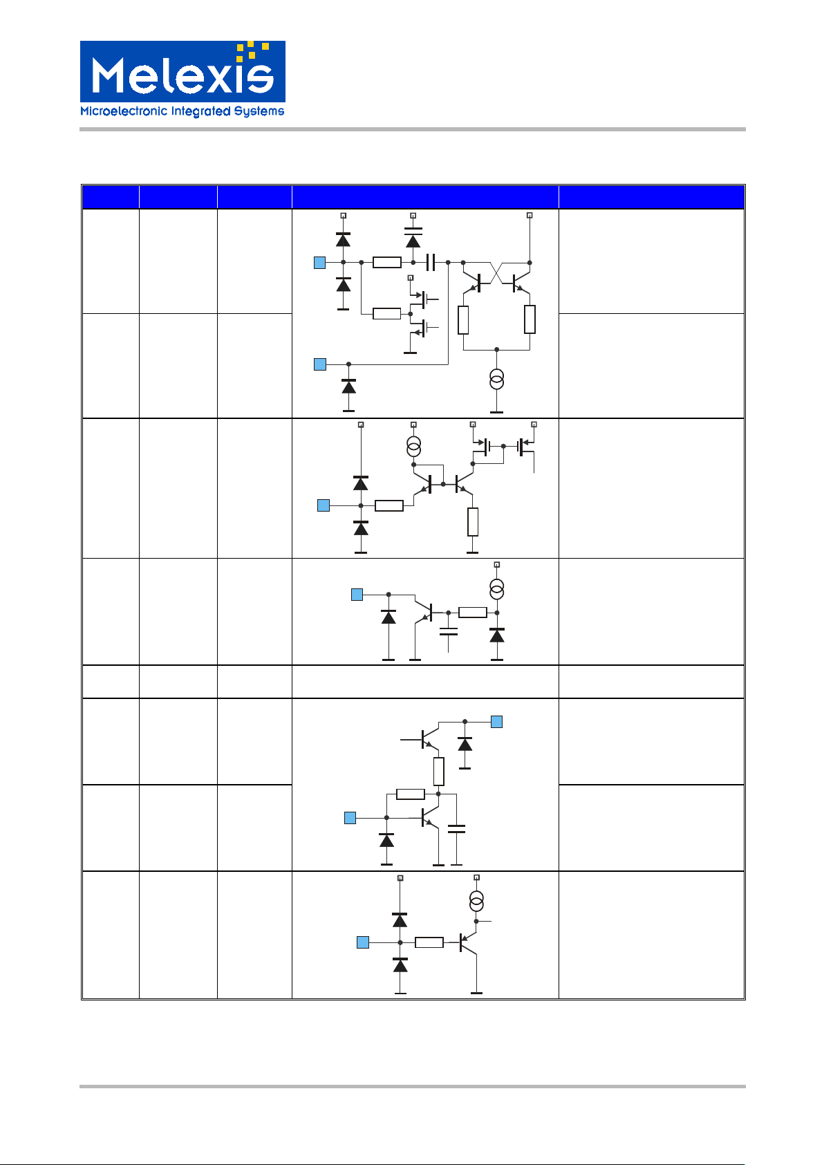
Pin Definition and Descripti on
Pin No. Name I/O Type Functional Schematic Description
1 IN_IFA input
3.1k3.1k
IN_IFA
1
VCC
140µA
VEE
2.2k
IF amplifier input, approx.
2
kΩ single-ended
2 VCC_IF supply positive supply of LNA, MIX,
IFA, FSK Demodulator, PA,
OA1 and OA2
3 IN_DEM analog I/O
VCC
100µA
10µA
VEE
IN_DEM
3
77k
1.5p
IF amplifier output and demodulator input, connection
to external ceramic discriminator
4 INT2 output integrator output OA2
8 OUT_DTA output
VCC
VEE
INT2
4
8
OUT_DTA
output OA1
5 INT1 input inverting inputs OA1 and
OA2
6 OUT_DEM analog I/O
OA2
bias
VEE
VCC
INT1
5
VEE
OUT_DEM
6
VCC
120
120
VEE
VCC
120
10.5p
10.5p
520k 520k
1k
OA1
+
200k
demodulator output and noninverting input OA1
7 RSSI output
VCC
VEE
RSSI
7
120
VEE
VCC
5µA
5µA
RSSI output
TH7120
300 to 930MHz
FSK/FM/ASK Transceiver
3901007120 Page 5 of 28 Data Sheet
Rev. 005 Jan. 2002
P
R
E
L
I
M
I
N
A
R
Y
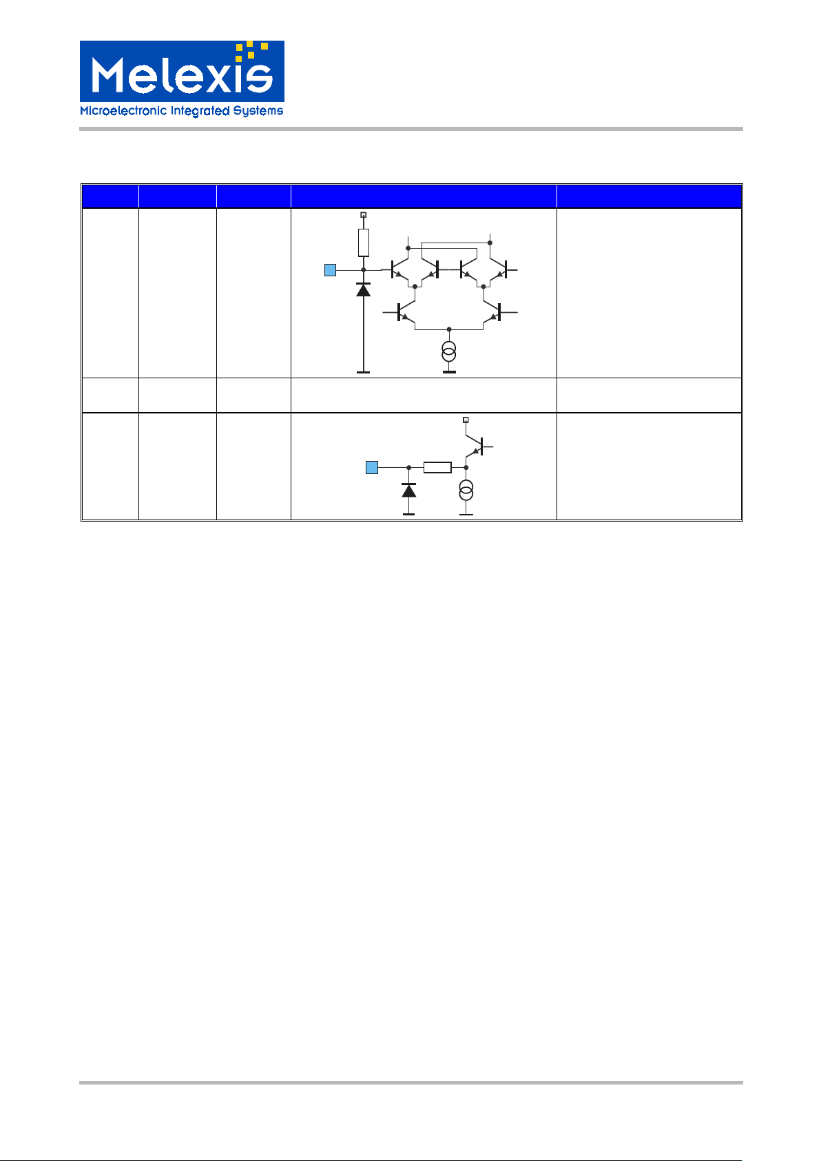
Pin No. Name I/O Type Functional Schematic Description
9 VEE_RO ground ground of RO
10 RO analog I/O
40p
VEE
VCC
RO
10
2.6µA
39k
40p
RO input, base of bipolar
transistor
11 FSK_SW analog I/O
VCC
VEE
FSK_SW
11
FSK pulling pin, switch to
ground or OPEN
12 IN_DTA input ASK/FSK modulation data
input, pull down resistor
120kΩ
15 RE/SCLK input receiver enable input / clock
input for the shift register,
pull down resistor 120kΩ
16 TE/SDTA input
VEE
VCC
IN_DTA
12
RE/SCLK
15
16
TE/SDTA
120k
120
transmitter enable input /
serial data input, pull down
resistor 120kΩ
13 ASK/FSK input ASK/FSK mode select input
17 FS0/SDEN input
VEE
VCC
ASK/FSK
13
17
FS0/SDEN
120
frequency select input / serial data enable input
14 VCC_DIG supply positive supply of serial port
and control logic
18 VEE_DIG ground ground of serial port and
control logic
19 FS1/LD input
VEE
VCC
FS1/LD
19
120
frequency select input / lock
detector output
20 VCC_PLL supply positive supply of PLL fre-
quency synthesizer
22 VEE_PLL ground ground of PLL frequency
synthesizer
TH7120
300 to 930MHz
FSK/FM/ASK Transceiver
3901007120 Page 6 of 28 Data Sheet
Rev. 005 Jan. 2002
P
R
E
L
I
M
I
N
A
R
Y
Pin No. Name I/O Type Functional Schematic Description
21 LF analog I/O charge pump output, con-
nection to external loop filter
23 TNK_LO analog I/O
120
10k
6.3p
VCC
VCC
VCC
VEE
33 33
VEE
LF
21
TNK_LO
23
VCO open-collector output,
connection to external LC
tank
24 PS_PA analog I/O
VEE VEE
VCC VCC
120
PS_PA
24
power-setting input
25 OUT_PA output
VEE VEE
VCC
OUT_PA
25
power amplifier opencollector output
27 VEE_LNA ground ground of LNA and PA
28 OUT_LNA output LNA open-collector output,
connection to external LC
tank at RF
26 IN_LNA input
40p
VEE
VEE
3.8k
OUT_LNA
28
bias
37
IN_LNA
26
LNA input,
approx. 50Ω single-ended
29 GAIN_LNA input
VCC
VEE
GAIN_LNA
29
120
LNA gain control input
TH7120
300 to 930MHz
FSK/FM/ASK Transceiver
3901007120 Page 7 of 28 Data Sheet
Rev. 005 Jan. 2002
P
R
E
L
I
M
I
N
A
R
Y
Pin No. Name I/O Type Functional Schematic Description
30 IN_MIX input
VCC
210
bias
LO
IN_MIX
30
VEE VEE
mixer input, approx. 200Ω
single-ended
31 VEE_IF ground ground of IFA, Demodulator,
OA1 and OA2
32 OUT_MIX output
VCC
VEE
OUT_MIX
32
100
mixer output, approx. 330Ω
single-ended
TH7120
300 to 930MHz
FSK/FM/ASK Transceiver
3901007120 Page 8 of 28 Data Sheet
Rev. 005 Jan. 2002
P
R
E
L
I
M
I
N
A
R
Y
Stand-Alone Fixed-Frequency Operation
After power up the transceiver is set to fixed-frequency mode. In this mode, pins FS0/SDEN and FS1/LD
must be connected to V
EE
or VCC to set the desired frequency of operation. The logic levels at pins FS0/SDEN
and FS1/LD must not be changed after power up in or der to remain in fixed-f requency mode. The default
settings of the control word bits in stand-alone mode are described in the frequency selection table.
Frequency Selection
Channel frequency 433.92 MHz 868.3 MHz 315 MHz 915 MHz
FS0/SDEN
1010
FS1/LD
0011
Reference oscillator frequency
7.1505 MHz
R counter ratio in RX mode
16 16 18 30
PFD frequency in RX mode
446.91 kHz 446.91 kHz 397.25 kHz 238.35 kHz
N/A counter ratio in RX mode
947 1919 766 3794
VCO frequency in RX mode
423.22 MHz 857.60 MHz 304.30 MHz 904.30 MHz
RX frequency
433.92 MHz 868.30 MHz 315.00 MHz 915.00 MHz
R counter ratio in TX mode
16 16 18 30
PFD frequency in TX mode
446.91 kHz 446.91 kHz 397.25 kHz 238.35 kHz
N/A counter ratio in TX mode
971 1943 793 3839
VCO frequency in TX mode
433.92 MHz 868.30 MHz 315.00 MHz 915.00 MHz
TX frequency
433.92 MHz 868.30 MHz 315.00 MHz 915.00 MHz
IF frequency in RX mode
10.7 MHz 10.7 MHz 10.7 MHz 10.7 MHz
TH7120
300 to 930MHz
FSK/FM/ASK Transceiver
3901007120 Page 9 of 28 Data Sheet
Rev. 005 Jan. 2002
P
R
E
L
I
M
I
N
A
R
Y
Default Register Settings After Power-up
Bits
A-word
symbols
Channel
‘00’
868.3
MHz
Channel
‘01’
433.92
MHz
Channel
‘10’
915.0
MHz
Channel
‘11’
315.0
MHz
B-word
symbols
Channel
‘00’
868.3
MHz
Channel
‘01’
433.92
MHz
Channel
‘10’
915.0
MHz
Channel
‘11’
315.0
MHz
21 not used 0 not used 0
20 DI_MODE 0 not used 0
19 MODUL 0 EnDelPLL 1
18 HighCur 0 LNAHYST 1
17
LOCK_MODE
0 EnAdj 0
16 PA_AUTO 0 EnFM 0
15 Pow1 1 Max2 1
14 Pow0 1 Max1 1
13 MIXG 1 Max0 1
12 LNAG 1 Min2 0
11 TE 0 Min1 1
10 RE 0 Min0 1
9 RR9 0 0 0 0 RT9 0 0 0 0
8 RR8 0 0 0 0 RT8 0 0 0 0
7 RR7 0 0 0 0 RT7 0 0 0 0
6 RR6 0 0 0 0 RT6 0 0 0 0
5 RR5 0 0 0 0 RT5 0 0 0 0
4 RR4 1 1 1 1 RT4 1 1 1 1
3 RR3 0 0 1 0 RT3 0 0 1 0
2 RR2 0 0 1 0 RT2 0 0 1 0
1 RR1 0 0 1 1 RT1 0 0 1 1
0 RR0 0 0 0 0 RT0 0 0 0 0
Bits
C-word
symbols
Channel
‘00’
868.3
MHz
Channel
‘01’
433.92
MHz
Channel
‘10’
915.0
MHz
Channel
‘11’
315.0
MHz
B-word
symbols
Channel
‘00’
868.3
MHz
Channel
‘01’
433.92
MHz
Channel
‘10’
915.0
MHz
Channel
‘11’
315.0
MHz
21 LNAGI_E 0
MODUL_CTR
0
20 POLAR 0 LD_TM1 1
19 High2 0 0 0 0 LD_TM0 0
18 High1 1 1 1 1 ER_TM1 0
17 UP 1 0 1 0 ER_TM0 0
16 NR16 0 0 0 0 NT16 0 0 0 0
15 NR15 0 0 0 0 NT15 0 0 0 0
14 NR14 0 0 0 0 NT14 0 0 0 0
13 NR13 0 0 0 0 NT13 0 0 0 0
12 NR12 0 0 0 0 NT12 0 0 0 0
11 NR11 0 0 1 0 NT11 0 0 1 0
10 NR10 1 0 1 0 NT10 1 0 1 0
9 NR9 1 1 1 1 NT9 1 1 1 1
8 NR8 1 1 0 0 NT8 1 1 0 1
7 NR7 0 1 1 1 NT7 1 1 1 0
6 NR6 1 0 1 1 NT6 0 1 1 0
5 NR5 1 1 0 1 NT5 0 0 1 0
4 NR4 1 1 1 1 NT4 1 0 1 1
3 NR3 1 0 0 1 NT3 0 1 1 1
2 NR2 1 0 0 1 NT2 1 0 1 0
1 NR1 1 1 1 1 NT1 1 1 1 0
0 NR0 1 1 0 0 NT0 1 1 1 1
 Loading...