

MELEXIS TH71101 Datasheet

TH71101
315/433MHz
FSK/FM/ASK Receiver
Features
! Single superhet architecture for low external component count
! FSK for digital data and FM reception for analog signal transmission
! FM/FSK demodulation with phase-coincidence demodulator
! Low current consumption in active mode and very low standby current
! Switchable LNA gain for improved dynamic range
! RSSI allows signal strength indication and ASK detection
! Surface mount package LQFP32
Ordering Information
Part No. Temperature Range Package
TH71101 -40 °C to 85°C LQFP32
Application Examples
! General digital and analog 315 MHz or 433 MHz ISM band usage
! Low-power telemetry
! Alarm and security systems
! Keyless car and central locking
! Pagers
Technical Data Overview
! Input frequency range: 300 MHz to 450 MHz
! Power supply range: 2.5 V to 5.5 V at 315 MHz and 2.7 V to 5.5 V at 433 MHz
! Temperature range: -40 °C to +85 °C
! Operating current: 6.5 mA at low gain and 8.2 mA at high gain mode
! Standby current: < 100 nA
! Sensitivity: -111 dBm
! Sensitivity: -104 dBm
! Range of IF: 455 kHz to 21.4 MHz
! Maximum input level: –10 dBm at ASK and 0 dBm at FSK
! Image rejection: > 55 dB (e.g. with SAW front-end filter and at 10.7 MHz IF)
! Spurious emission: < -70 dBm
! Input frequency acceptance: ±50 kHz (with AFC option)
! RSSI range: 70 dB
! Frequency deviation range: ±5 kHz to ±120 kHz
! Maximum data rate: 80 kbit/s NRZ
! Maximum analog modulation frequency: 15 kHz
1)
at ± 8 kHz FSK deviation, BER = 3⋅10-3 and phase-coincidence demodulation
2)
at ± 50 kHz FSK deviation, BER = 3⋅10-3 and phase-coincidence demodulation
1)
with 40 kHz IF filter BW (incl. SAW front-end filter loss)
2)
with 150 kHz IF filter BW (incl. SAW front-end filter loss)
TH71101 Data Sheet Page 1 of 20 Nov. 2001
3901071101 Rev. 005
TH71101
315/433MHz
FSK/FM/ASK Receiver
General Description
The TH71101 receiver IC consists of the following building blocks
" PLL synthesizer (PLL SYNTH) for generation of the local oscillator signal LO
" Parts of the PLL SYNTH are the high-frequency VCO1, the feedback divider DIV_16,
a phase-frequency detector (PFD) with charge pump (CP) and a crystal-based reference oscillator (RO)
" Low-noise amplifier (LNA) for high-sensitivity RF signal reception
" First mixer (MIX1) for down-conversion of the RF signal to the IF
" IF pre amplifier which is a mixer cell (MIX2) that operates as an amplifier
" IF amplifier (IFA) to amplify and limit the IF signal and for RSSI generation
" Phase coincidence demodulator (DEMOD) with third mixer (MIX3) to demodulate the IF signal
" Operational amplifier (OA) for data slicing, filtering and ASK detection
" Bias circuitry for bandgap biasing and circuit shutdown
With the T H71101 receiver c hip, various circuit c onfigurations c an be arranged in or der to m eet a num ber of
different custom er requirements . For FM/FSK reception the IF tank used in the phase coincidence dem odulator can be constituted either by a ceramic resonator or an LC tank (optionally with a varactor diode to create
an AFC circuit). In ASK configuration, the RSSI signal is feed to an ASK detector, which is constituted by the
operational amplifier.
Demodulation Type of receiver
FM / FSK
FM / FSK
ASK
A double-conversion variant, called TH71102, is also available. This receiver IC allows a higher degree of
image rejection, achieved in conj unction with an RF frontend filter. Both RXICs have the sam e die. At the
TH71102, the second mixer (MIX2) is used to down-convert the first IF (IF1) to the second IF (IF2). At the
TH71101, MIX2 operates as an amplifier.
Efficient RF frontend f iltering is realized by using a SAW, ceramic or helix filter in front of the LNA and by
adding an LC filter at the LNA output.
narrow-band RX with ceramic demodulation tank
wide-band RX with LC demodulation tank
RX with RSSI-based demodulation
TH71101 Data Sheet Page 2 of 20 Nov. 2001
3901071101 Rev. 005
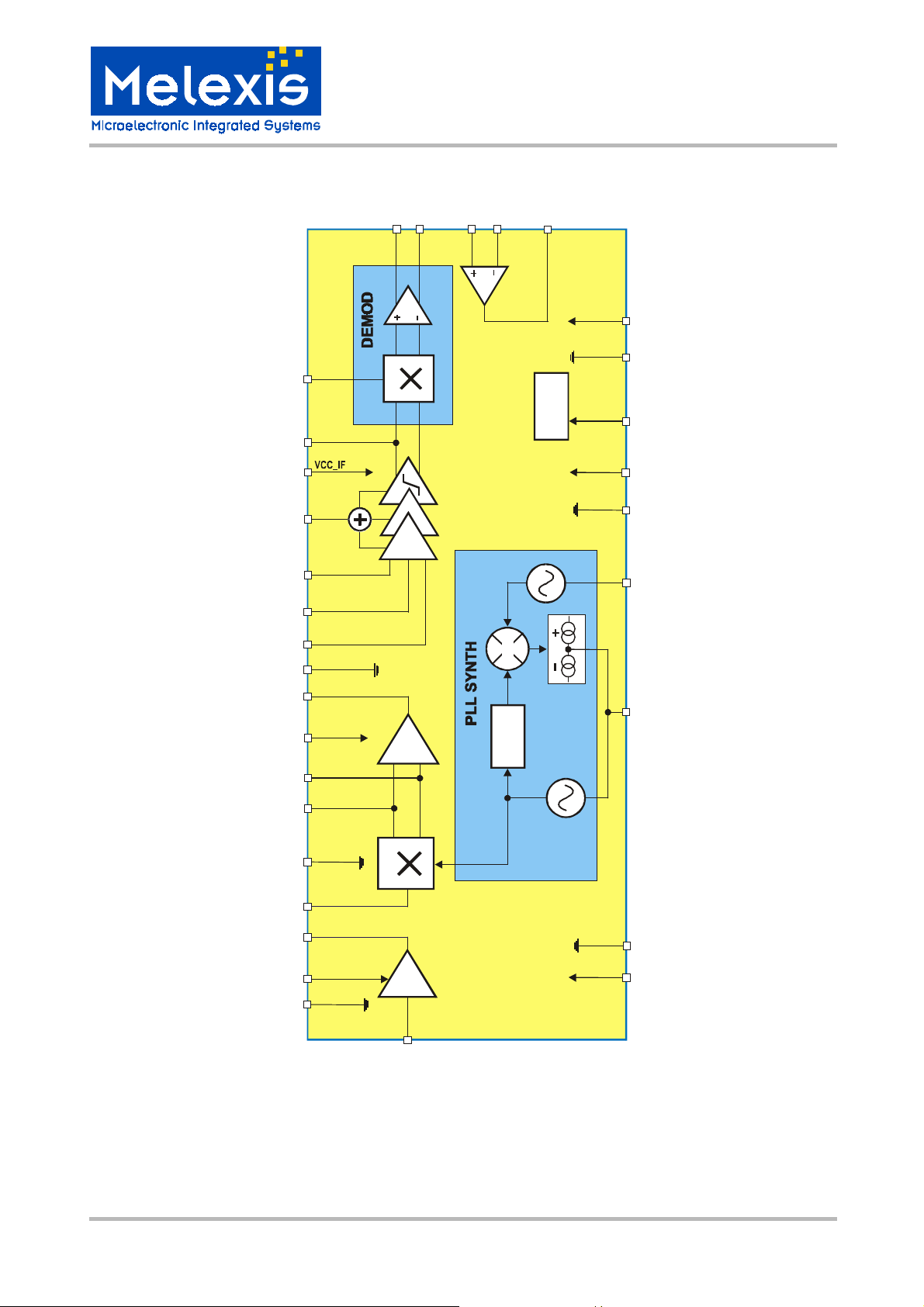
Block Diagram
TH71101
315/433MHz
FSK/FM/ASK Receiver
IN_DEM
OUT_IFA
14
RSSI
21
FPC2
13 15 16
FBC1
12
IN_IFA
11
VEE_IF
10
OUT_MIX2
93
VCC_MIX
8
IF1N
7
IF1P
6
24
23
OUTP
OUTN
20
19
OAP
OAN
18
OUT_OA
OA
VCC_BIAS
17
VEE_BIAS
22
MIX3
ENRX
BIAS
28
VCC_PLL
27
VEE_RO
25
IFA
RO
RO
26
PFD
IF
CP
MIX2
IF
DIV_16
LF
29
VEE_MIX
5
IN_MIX1
4
OUT_LNA
GAIN_LNA
2
VEE_LNAC
1
LO
MIX1
LNA
IN_LNA
31
VCO1
VEE_LNA
30
VCC_LNA
32
Fig. 1: TH71101 block diagram
TH71101 Data Sheet Page 3 of 20 Nov. 2001
3901071101 Rev. 005
TH71101
315/433MHz
FSK/FM/ASK Receiver
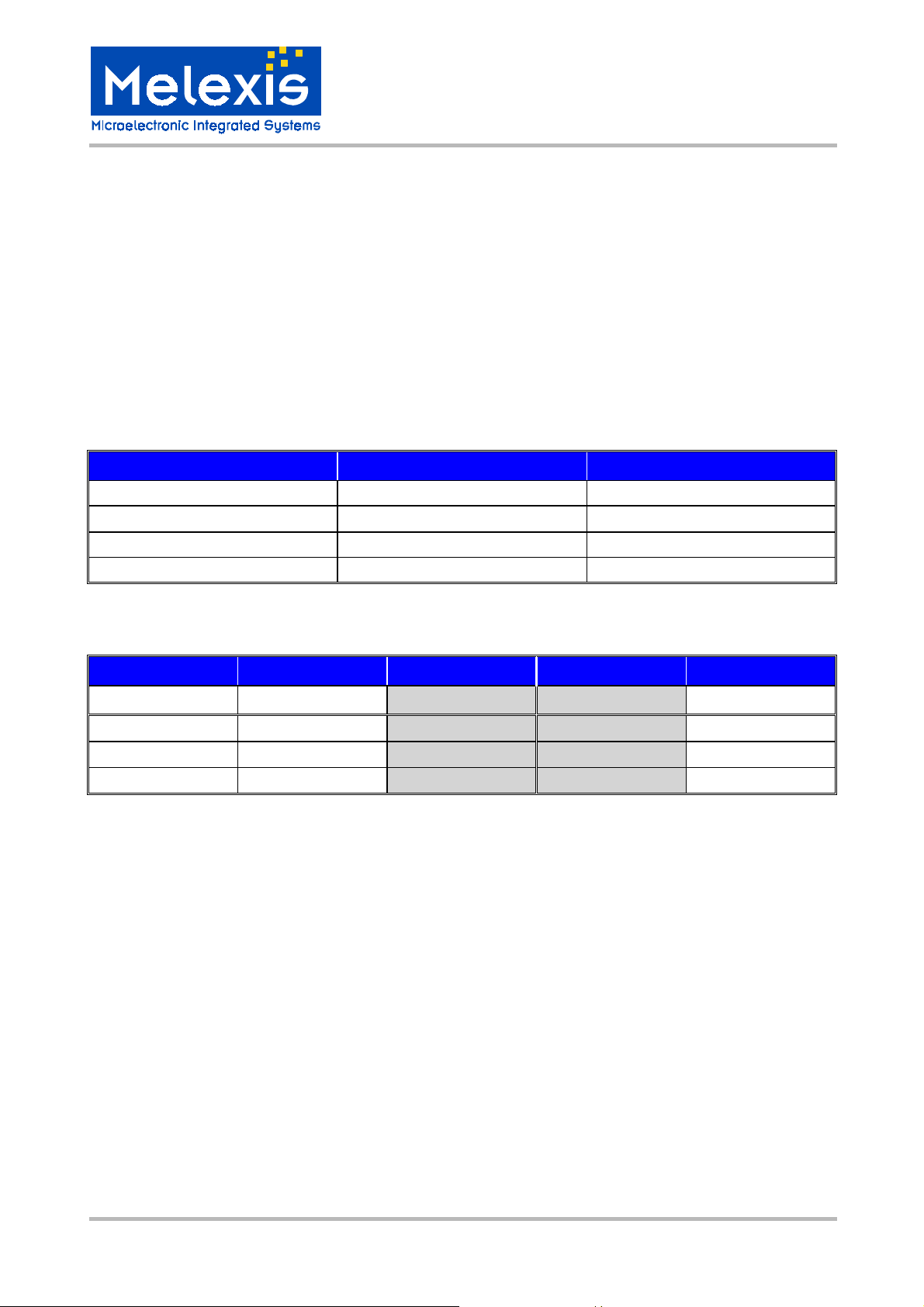
Frequency Planning
Frequency planning is straightforward for single-conversion applications because there is only one IF that
might be chosen, and then the only possible choice is low-side or high-side inj ection of the LO signal (which
is now the one and only LO signal in the receiver).
The receiver’s single-conversion architecture requires careful frequency planning. Besides the desired RF
input signal, there are a number of s purious signals that may cause an undesired response at the output.
Among them is the image of the RF signal that must be suppressed by the RF front-end filter.
By using the internal PLL synthesizer of the TH71101 with the fixed feedback divider ratio of N = 16 (DIV_16),
two types of down-conversion are possible: low-side injection of LO and high-side injection of LO . The following table summarizes some equations that are useful to calc ulate the crystal reference frequency (REF),
the IF and the LO frequency respectively, for a given RF.
Injection type low high
REF (RF – IF)/16 (RF + IF)/16
LO
IF RF – LO LO – RF
RF image RF – 2IF RF + 2IF
16•REF 16•REF
The following table depicts crystal, LO and image signals considering the examples of 315 MHz and
433.6 MHz RF reception at IF = 10.7 MHz.
Signal type RF = 315 MHz RF = 315 MHz RF = 433.6 MHz RF = 433.6 MHz
Injection type low
REF / MHz 19.01875
LO / MHz 304.3
RF image / MHz 293.6
The selection of the reference crystal frequency is based on some as sumptions. As for example: the image
frequency should not be in a radio band where strong interfering signals might occur (bec ause they could
represent parasitic receiving s ignals), the LO s ignal should be in the range of 300 MHz to 430 MHz (because
this is the optimum frequency range of the VCO1). Furthermore the IF should be as high as possible to
achieve highest RF image rejec tion. The columns in bold depict the selected frequency plans to rec eive at
315 MHz and 433.6 MHz, respectively.
high low
20.35625 26.43125
325.7 422.9
336.4 412.2
high
27.76875
444.3
455.0
TH71101 Data Sheet Page 4 of 20 Nov. 2001
3901071101 Rev. 005
TH71101
315/433MHz
FSK/FM/ASK Receiver
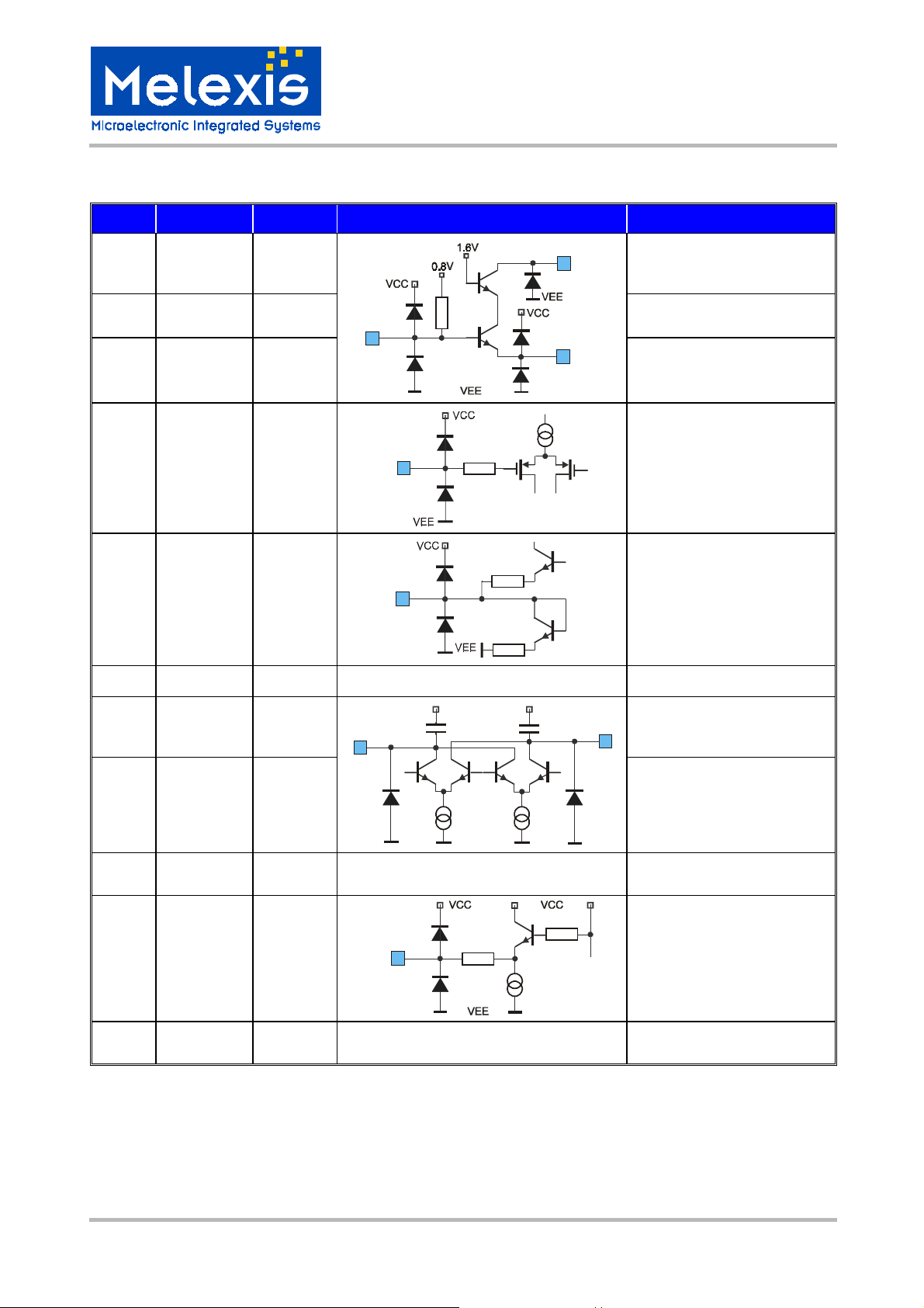
Pin Definition and Descripti on
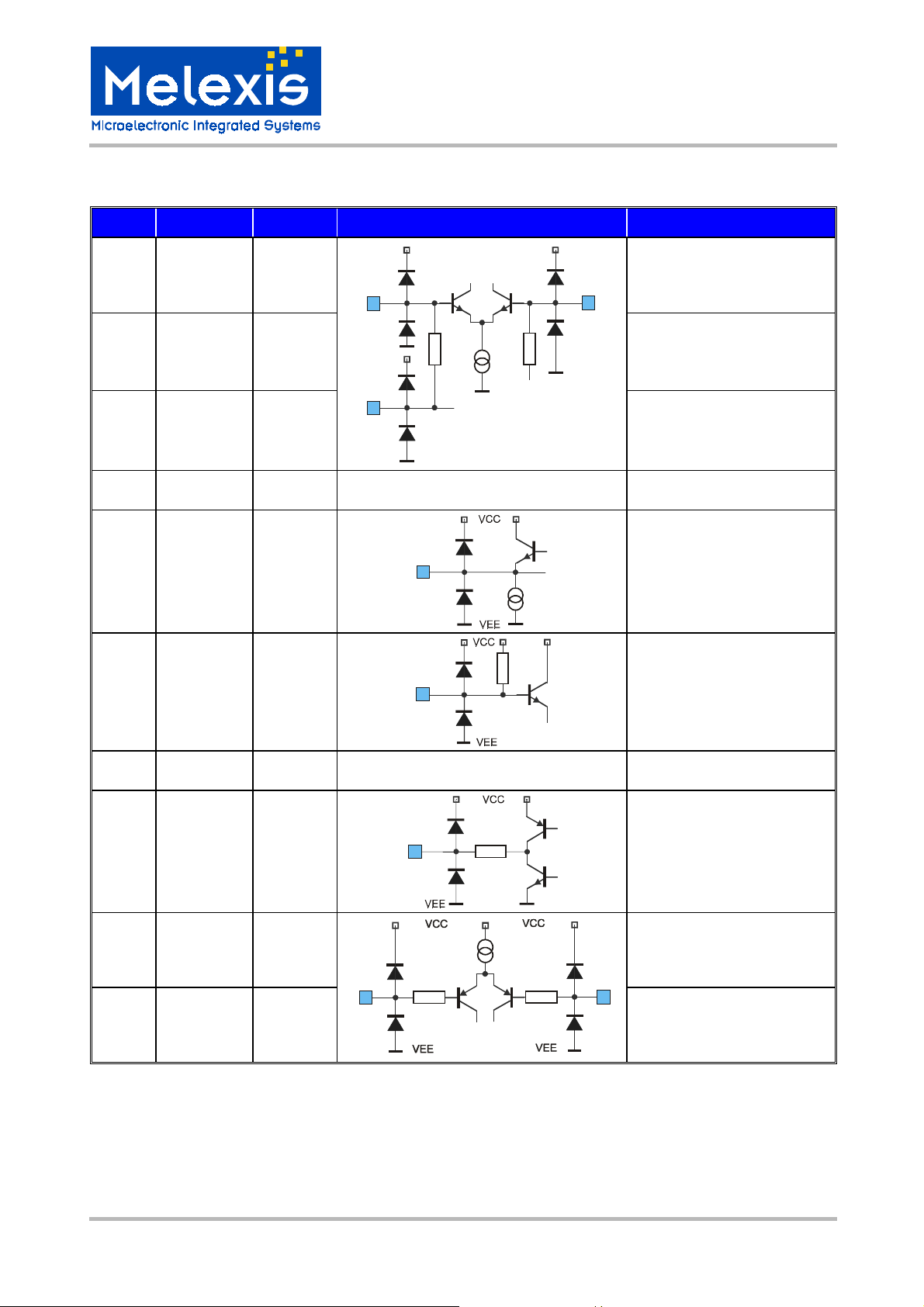
Pin No. Name I/O Type Functional Schematic Description
13
Ω
OUT_LNA
3
VEE_LNAC
1
LNA open-collector output,
to be connected to external
LC tank that resonates at RF
LNA input, approx.
26Ω single-ended
ground of LNA core
(cascode)
LNA gain control (CMOS
input with hysteresis)
MIX1 input, approx. 33Ω
single-ended
3 OUT_LNA analog
output
31 IN_LNA analog
input
1 VEE_LNAC ground
2 GAIN_LNA analog
input
4 IN_MIX1 analog
input
IN_LNA
31
GAIN_LNA
2
IN_MIX1
5k
400
Ω
4
Ω
13
500µA
5 VEE_MIX ground LNA biasing ground
20p
VCC
20p
IF1N
connected to external LC
tank that resonates at first IF
7
open-collector output, to be
6 IF1P analog I/O open-collector output, to be
IF1P
7 IF1N analog I/O
6
connected to external LC
2x500µA
VEE
VEE
tank that resonates at first IF
8 VCC_MIX supply MIX1 and MIX2 positive
supply
9 OUT_MIX2 analog
output
OUT_MIX2
9
130
6.8k
Ω
230µA
MIX2 output, approx. 330Ω
output impedance
10 VEE_IF ground ground for MIX2, IFA and
DEMOD
TH71101 Data Sheet Page 5 of 20 Nov. 2001
3901071101 Rev. 005
TH71101
315/433MHz
FSK/FM/ASK Receiver
Pin No. Name I/O Type Functional Schematic Description
11 IN_IFA analog
input
VCC
IN_IFA
VCC
IFA input, approx. 2.2kΩ
input impedance
FBC1
12
IFA feedback capacitor
VEE
to be connected to external
IFA feedback capacitor
positive supply for IFA,
11
VEE
FBC2
13
VCC
VEE
2.2k
2.2k
200µA
VEE
12 FBC1 analog I/O to be connected to external
13 FBC2 analog I/O
14 VCC_IF supply
DEMOD
15 OUT_IFA analog I/O
IFA output and MIX3 input
(of DEMOD)
OUT_IFA
15
40µA
16 IN_DEM analog
input
IN_DEM
16
47k
DEMOD input, to MIX3 core
17 VCC_BIAS supply
positive supply of general
bias system and OA
18 OUT_OA analog
output
OUT_OA
Ω
50
OA output, 40uA current
drive capability
18
19 OAN analog
input
20 OAP analog
input
OAN
19
20µA
Ω
50
Ω
50
negative OA input, input
voltage limited to approx.
between pins OAP
pp
OAP
0.7 V
and OAN
negative OA input, input
20
voltage limited to approx.
0.7 V
between pins OAP
pp
and OAN
TH71101 Data Sheet Page 6 of 20 Nov. 2001
3901071101 Rev. 005
 Loading...