

MELEXIS TH7110 Datasheet

TH7110
315/433MHz
FSK/FM/ASK Receiver
Features
! Double superhet architecture for high degree of image rejection
! FSK for digital data and FM reception for analog signal transmission
! FM/FSK demodulation either with phase-coincidence or PLL demodulator
! Low current consumption in active mode and very low standby current
! Switchable LNA gain for improved dynamic range
! AFC feature allows wide carrier frequency acceptance range
! RSSI allows signal strength indication and ASK detection
! Surface mount package LQFP44
Ordering Information
Part No. Temperature Range Package
TH7110 -40 °C to 85 °C LQFP44
Application Examples
! General digital and analog 315 MHz or 433 MHz ISM band usage
! Low-power telemetry
! Alarm and security systems
! Keyless car and central locking
! Pagers
Technical Data Overview
! Input frequency range: 300 MHz to 450 MHz
! Power supply range: 2.5 V to 5.5 V for double conversion and 2.7 V to 5.5 V for single conversion
! Temperature range: -40 °C to +85 °C
! Operating current: 6.5 mA at low gain and 8.2 mA at high gain mode
! Standby current: < 100 nA
! Sensitivity: -111 dBm
! Sensitivity: -104 dBm
! Range of first IF: 10 MHz to 80 MHz
! Range of second IF: 455 kHz to 21.4 MHz
! Maximum input level: –10 dBm at ASK and 0 dBm at FSK
! Image rejection: > 65 dB (e.g. with SAW front-end filter and at 10.7 MHz 2
! Spurious emission: < -70 dBm
! Input frequency acceptance: ±50 kHz (with AFC option)
! RSSI range: 70 dB
! Frequency deviation range: ±5 kHz to ±120 kHz
! Maximum data rate: 80 kbit/s NRZ
! Maximum analog modulation frequency: 15 kHz
1)
at ± 8 kHz FSK deviation, BER = 3⋅10-3 and phase-coincidence demodulation
2)
at ± 50 kHz FSK deviation, BER = 3⋅10-3 and phase-coincidence demodulation
1)
with 40 kHz second IF filter BW (incl. SAW front-end filter loss)
2)
with 150 kHz second IF filter BW (incl. SAW front-end filter loss)
nd
IF)
TH7110 Data Sheet Page 1 of 20 Nov. 2001
3901007110 Rev. 005
TH7110
315/433MHz
FSK/FM/ASK Receiver
General Description
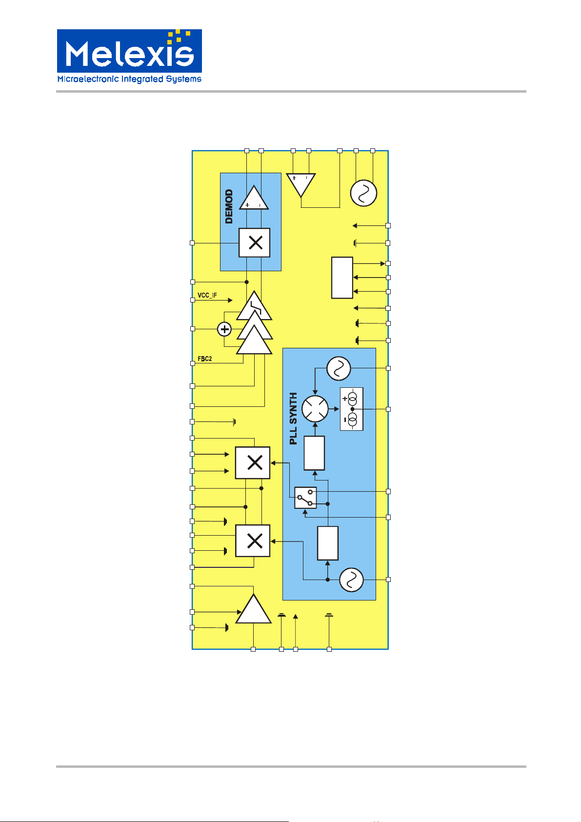
The TH7110 receiver IC consists of the following building blocks:
" PLL synthesizer (PLL SYNTH) for generation of the first and second local oscillator signals LO1 and LO2
" Parts of the PLL SYNTH are the high-frequency VCO1, the feedback dividers DIV_8 and DIV_2,
a phase-frequency detector (PFD) with charge pump (CP) and a crystal-based reference oscillator (RO)
" Low-noise amplifier (LNA) for high-sensitivity RF signal reception
" First mixer (MIX1) for down-conversion of the RF signal to the first IF (IF1)
" second mixer (MIX2) for down-conversion of the IF1 to the second IF (IF2)
" IF amplifier (IFA) to amplify and limit the IF2 signal and for RSSI generation
" Phase coincidence demodulator (DEMOD) with third mixer (MIX3) to demodulate the IF signal
" Operational amplifier (OA) for data slicing, filtering, ASK detection and automatic-frequency control (AFC)
" Bias circuitry for bandgap biasing and circuit shutdown
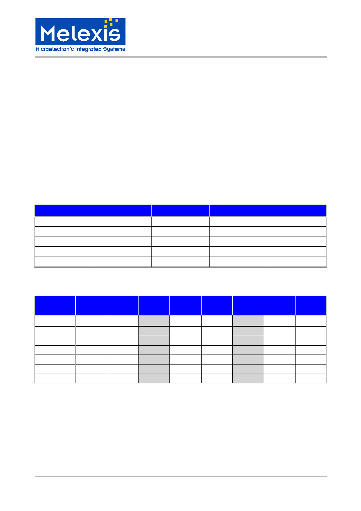
With the T H7110 receiver chip, various circuit c onfigurations can be arranged in order to m eet a number of
different custom er requirements . For FM/FSK reception the IF tank used in the phase coincidence dem odulator can be constituted either by a ceramic resonator or an LC tank (optionally with varactor to create an AFC
circuit). In PLL demodulator configuration, the multiplier MIX3 f orms a phase com parator. In ASK c onfiguration, the RSSI signal is feed to an ASK detector, which is c onstituted by the operational amplif ier. T he sec ond
VCO (VCO2) can be used either as the VCO of a PLL demodulator or as the LO 2 source of a second external PLL in a multi-channel system. The following table briefly summarizes the various configurations.
Single-conversion configuration Double-conversion configuration
FM/FSK
FM/FSK
FM/FSK
FM/FSK
ASK
ASK
The preferred superheter odyne configuration is double conversion where MIX1 and MIX2 are driven by the
internal local oscillator signals LO1 and LO 2, respectively. This allows a high degree of image rejection,
achieved in conjunction with an RF front-end filter. Eff icient RF front- end filtering is r ealized by using a SAW,
ceramic or helix filter in front of the LNA and by adding a LC filter at the LNA output.
It is also possible to use the T H7110 in single-conversion configur ation. This can be ac hieved by switching
the LO2 input of MIX2 from the on-chip PLL synthesizer to the pin IN_MIX2 by means of an internal switch
(done via pin SW_MIX2). Now MIX2 operates as an amplifier f or the IF1 signal if an external pull-down resistor at pin IN_MIX2 is added.
The same setting of MIX2 can be used for multi-channel applications. In this situation IN_MIX2 mus t be
driven by an external LO2 signal. This signal can be generated by the VCO2, which is mainly a bipolar transistor that can be configured as a varactor-tuned VCO. Furthermore, a second external PLL for channel
selection via LO2 tuning is required. This may be arranged by using a PLL synthesizer chip that can be controlled through a 3-wire bus serial interface. The reference signal for the external PLL synthesizer can be
directly taken from the crystal-based reference oscillator RO.
narrow-band RX with ceramic demodulation
tank
wide-band RX with LC demod. tank and AFC wide-band RX with LC demod. tank and AFC
extended sensitivity RX with PLL demodulator extended sensitivity RX with PLL demodulator
RX with RSSI-based demodulation RX with RSSI-based demodulation
narrow-band RX with ceramic demodulation
tank
multi-channel RX with ceramic demodulation
tank and external channel synthesizer
RX with RSSI-based demodulation and external channel synthesizer
TH7110 Data Sheet Page 2 of 20 Nov. 2001
3901007110 Rev. 005
Block Diagram
TH7110
315/433MHz
FSK/FM/ASK Receiver
IN_DEM
OUT_IFA
19 20
18
RSSI
29
17
FBC1
16
IN_IFA
151413
VEE_IF
OUT_MIX2
VCC_MIX2
12
VCC_MIX1
11
IF1N
10
IF1P
9
VEE_MIX1
8
CAP_MIX1
7
VEE_LNA
5
IN_MIX1
6
OUT_LNA
43
31
32
OUTP
OUTN
28
27
OAP
OAN
26
OUT_OA
23
24
VCO2_E
VCO2_B
OA
VCO2
VCC_BIAS
25
VEE_BIAS
MIX3
BIAS
VREF
ENRO
ENRX
VCC_PLL
VEE_RO
VEE_PLL
30
37 144
36
34
IFA
RO
ROLF2 SW_MIX2
35
LF1
PFD
IF2
CP
LO2
MIX2MIX1
IF1
LO1
DIV_2
IN_MIX2
switch
DIV_8
VCO1
39 332221 38
GAIN_LNA
VEE_LNAC
2
LNA
IN_LNA
42
VCC_LNA41VEE_LNA
VEE_VCO1
43
40
Fig. 1: TH7110 block diagram
TH7110 Data Sheet Page 3 of 20 Nov. 2001
3901007110 Rev. 005
TH7110
315/433MHz
FSK/FM/ASK Receiver
Frequency Planning
Frequency planning is straightforward for single-conversion applications because there is only one IF that
might be chosen, and then the only possible choice is low-side or high-side injection of the LO1 s ignal (which
is now the one and only LO signal in the receiver).
The receiver’s double-conver sion architecture requires careful frequenc y planning. Besides the desired RF
input signal, there are a number of s purious signals that may cause an undesired response at the output.
Among them are the image of the RF signal (that must be suppressed by the RF front-end f ilter), spurious
signals injected to the first IF ( IF1) and their im ages which could be m ixed down to the sam e sec ond IF (IF2)
as the desired RF signal (they must be suppressed by the LC filter at IF1 and/or by low-crosstalk design).
By configuring the TH7110 for double conversion and using its internal PLL synthesizer with fixed feedback
divider ratios of N1 = 8 (DIV_8) and N2 = 2 (DIV_2) , four types of down-conversion are possible: low-side
injection of LO1 and LO2 (low - low), LO1 low-side and LO2 high-side (low-high), LO1 high-side and LO2
low-side (high-low) or LO1 and LO2 high-s ide (high-high). T he following table sum m arizes som e equations
that are useful to calculate the crystal reference frequency (REF), the firs t IF (IF1) and the VCO1 or firs t LO
frequency (LO1), respectively, for a given RF and second IF (IF2).
Injection type high-high low-low high-low low-high
REF (RF – IF2)/14 (RF – IF2)/18 (RF + IF2)/14 (RF + IF2)/18
LO1
16•REF 16•REF 16•REF 16•REF
IF1 LO1 – RF RF – LO1 LO1 – RF RF – LO1
LO2
2•REF 2•REF 2•REF 2•REF
IF2 LO2 – IF1 IF1 – LO2 IF1 – LO2 LO2 – IF1
The following table depicts generated, desired, pos sible images and som e undesired s ignals cons idering the
examples of 315 MHz and 433.6 MHz RF reception at IF2 = 10.7 MHz.
Signal type RF = 315
MHz
Injection type high-high low-low
REF / MHz 21.73571 16.90556
LO1 / MHz 347.77143 270.48889
IF1 / MHz 32.77143 44.51111
LO2 / MHz 43.47143 33.81111
RF image/MHz 380.54286 225.97778
IF1 image/MHz 54.17143 23.11111
RF = 315
MHz
RF = 315
MHz
high-low
23.26429
372.22857
57.22857
46.52857
429.45714
35.82857
RF = 315
MHz
low-high high-high
18.09444 30.20714
289.51111 483.31429
25.48889 49.71429
36.18889 60.41429
264.02222 533.02857
46.88889 71.11429
RF =
433.6 MHz
RF =
433.6 MHz
low-low
23.49444
375.91111
57.68889
46.98889
318.22222
36.28889
RF =
433.6 MHz
high-low low-high
31.73571 24.68333
507.77143 394.93333
74.17143 38.66667
63.47143 49.36667
581.94286 356.26667
52.77143 60.06667
RF =
433.6 MHz
The selection of the ref erence crystal frequency is based on som e assumptions. As for example: the f irst IF
and the image frequencies should not be in a radio band where strong interfering signals might occur
(because they could represent parasitic receiving s ignals), the LO1 s ignal should be in the range of 300 MHz
to 430 MHz (because this is the optimum frequency range of the VCO1). Furtherm ore the first IF should be
as high as possible to achieve highest RF image rejection. The colum ns in bold depict the selec ted f r equenc y
plans to receive at 315 MHz and 433.6 MHz, respectively.
TH7110 Data Sheet Page 4 of 20 Nov. 2001
3901007110 Rev. 005
TH7110
315/433MHz
FSK/FM/ASK Receiver
Pin Definition and Descripti on
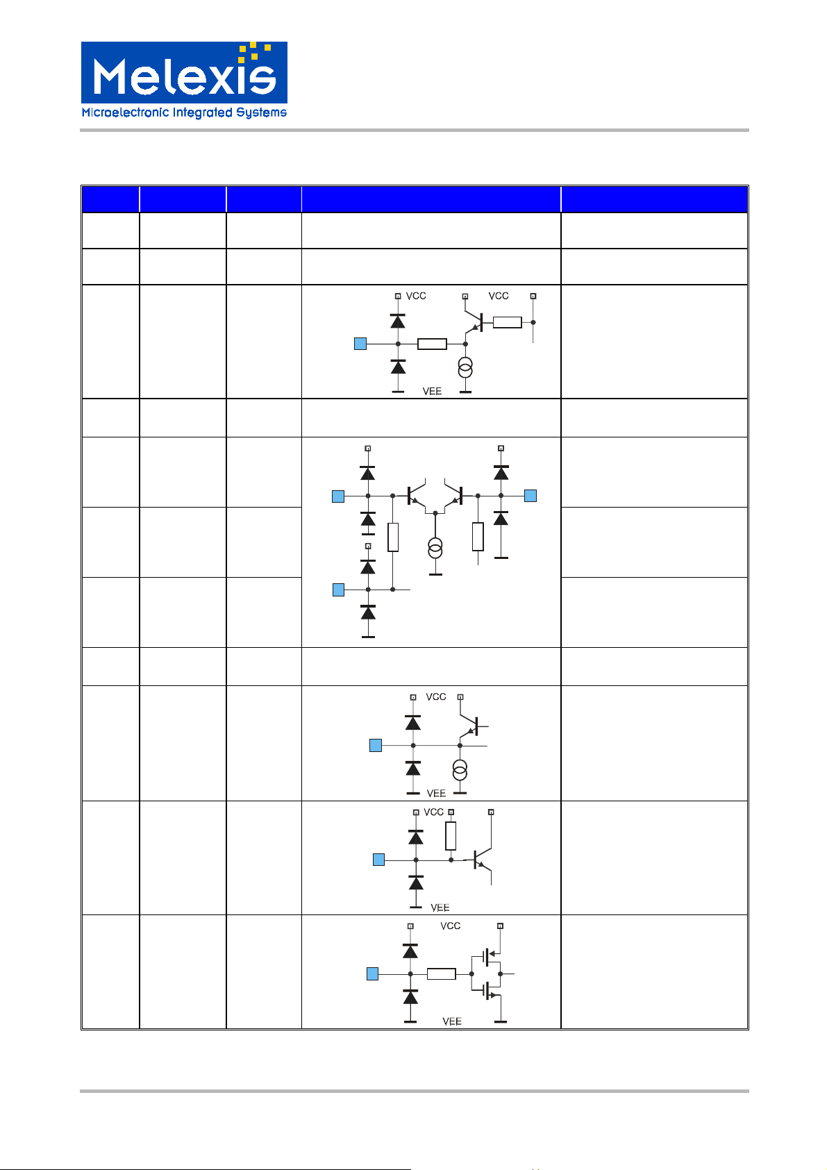
Pin No. Name I/O Type Functional Schematic Description
1 VREF analog
output
VREF
1
60k
reference voltage output,
approx. 1.23V
4 OUT_LNA analog
output
42 IN_LNA analog
input
2 VEE_LNAC ground
IN_LNA
42
5k
OUT_LNA
4
VEE_LNAC
2
LNA open-collector output,
to be connected to external
LC tank that resonates at RF
LNA input,
approx. 26Ω single-ended
ground of LNA core
(cascode)
3 GAIN_LNA analog
input
GAIN_LNA
3
400
Ω
LNA gain control (CMOS
input with hysteresis)
5 VEE_LNA ground LNA biasing ground
6 IN_MIX1 analog
input
7 CAP_MIX1 analog I/O
IN_MIX1
6
CAP_MIX1
7
Ω
13
Ω
13
500µA
40µA
Ω
330
MIX1 input, approx. 33Ω
single-ended
connection for MIX1
blocking capacitor
8 VEE_MIX1 ground MIX1 ground
20p
VCC
20p
IF1N
10
connected to external LC
tank that resonates at first IF
open-collector output, to be
9 IF1P analog I/O open-collector output, to be
IF1P
9
10 IF1N analog I/O
connected to external LC
VEE
2x500µA
VEE
tank that resonates at first IF
TH7110 Data Sheet Page 5 of 20 Nov. 2001
3901007110 Rev. 005
TH7110
315/433MHz
FSK/FM/ASK Receiver
Pin No. Name I/O Type Functional Schematic Description
11 VCC_MIX1 supply MIX1 positive supply
12 VCC_MIX2 supply MIX2 positive supply
13 OUT_MIX2 analog
output
OUT_MIX2
13
130
6.8k
Ω
230µA
MIX2 output, approx. 330Ω
output impedance
14 VEE_IF ground ground of MIX2, IFA and
DEMOD
2.2k
200µA
VCC
IFA input, approx. 2.2kΩ
input impedance
FBC1
16
IFA feedback capacitor
VEE
to be connected to external
IFA feedback capacitor
15 IN_IFA analog
VCC
input
IN_IFA
15
VEE
FBC2
17
VCC
2.2k
VEE
VEE
16 FBC1 analog I/O to be connected to external
17 FBC2 analog I/O
18 VCC_IF supply positive supply for IFA,
DEMOD and VCO2
19 OUT_IFA analog I/O
IFA output and MIX3 input
(of DEMOD)
OUT_IFA
19
40µA
20 IN_DEM analog
input
IN_DEM
20
47k
DEMOD input, to MIX3 core
21 SW_MIX2 digital
input
SW_MIX2
21
400
Ω
input selection for LO2 input
port of MIX2
TH7110 Data Sheet Page 6 of 20 Nov. 2001
3901007110 Rev. 005
 Loading...