

MELEXIS TH71072 Datasheet
Features
! Fully integrated, PLL-stabilized VCO
! Flexible frequency range from 310 MHz to 450 MHz
! ASK achieved by on/off keying of internal
power amplifier
! FM possible with external varactor
! Wide power supply range from 2.2 V to 5.5 V
! High over-all frequency accuracy
! Very low standby current
TH71072
315/433MHz
ASK Transmitter / LO Source
! Adjustable output power range from
-15 dBm to -1 dBm
! Adjustable current consumption from
4.8 mA to 11.5 mA
! Single-ended RF output
! Clock output for µC drive
! Conforms to EN 300 220 and similar
standard
Ordering Information
Part No. Temperature Range Package
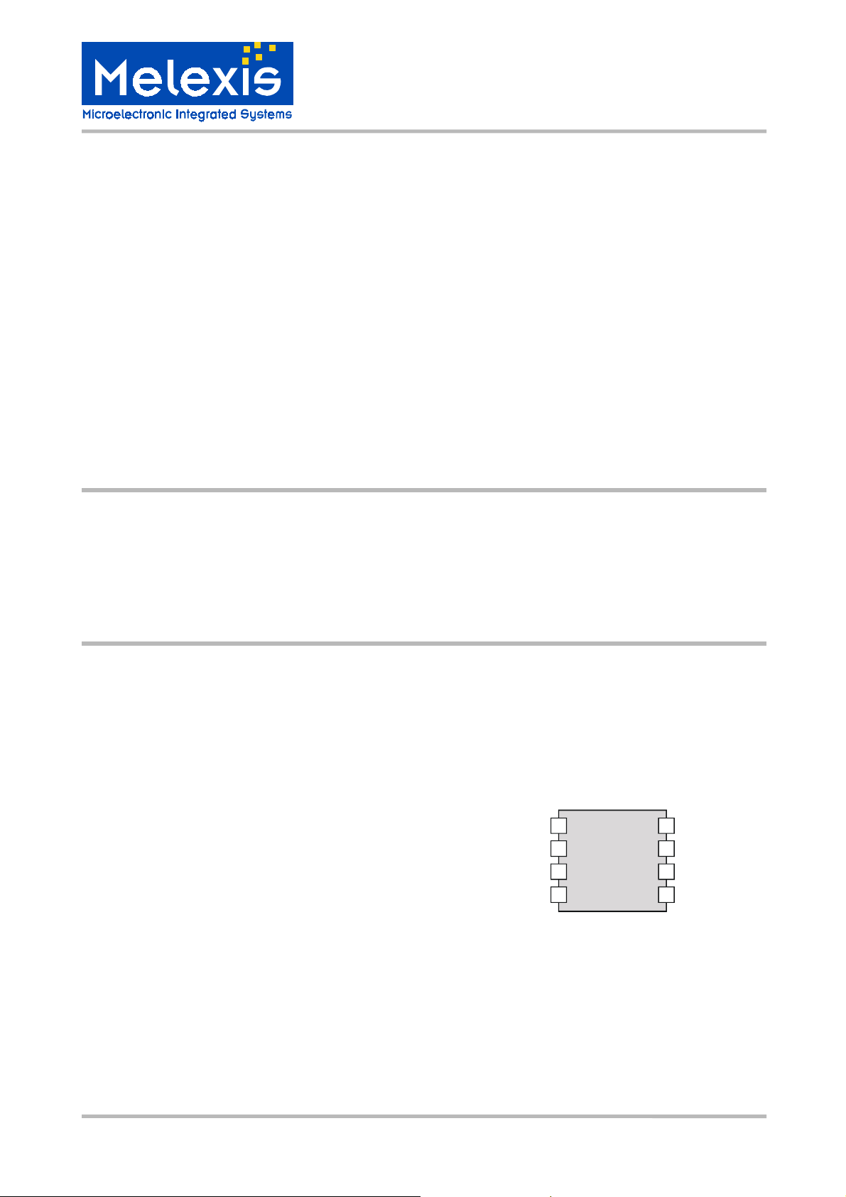
TH71072 -40 C° to 85 °C SOIC8
Application Examples Pin Description
! Keyless car and central locking
! Low-power telemetry
! Alarm and security systems
! General digital data transmission
! General analog audio signal transmission
! Local oscillator signal gener ation
LF
RO
ENTX
CKOUT
1
2
3
4
TH71072
VEE
8
7
OUT
6
VCC
PS/DATA
5
3901071072 Page 1 of 10 Data Sheet
Rev. 004 Dec. 2001
General Description
TH71072
315/433MHz
ASK Transmitter / LO Source
The TH71072 ASK transmitter IC is designed for
applications in the European 433MHz industrialscientific-m edical (ISM) band, according to the EN
300 220 telecommunications standard. It can also
be used for any other system with carrier
frequencies ranging from 310 MHz to 450 MHz
(e.g. for applications in the US 315MHz ISM band).
Theory of Operation
General
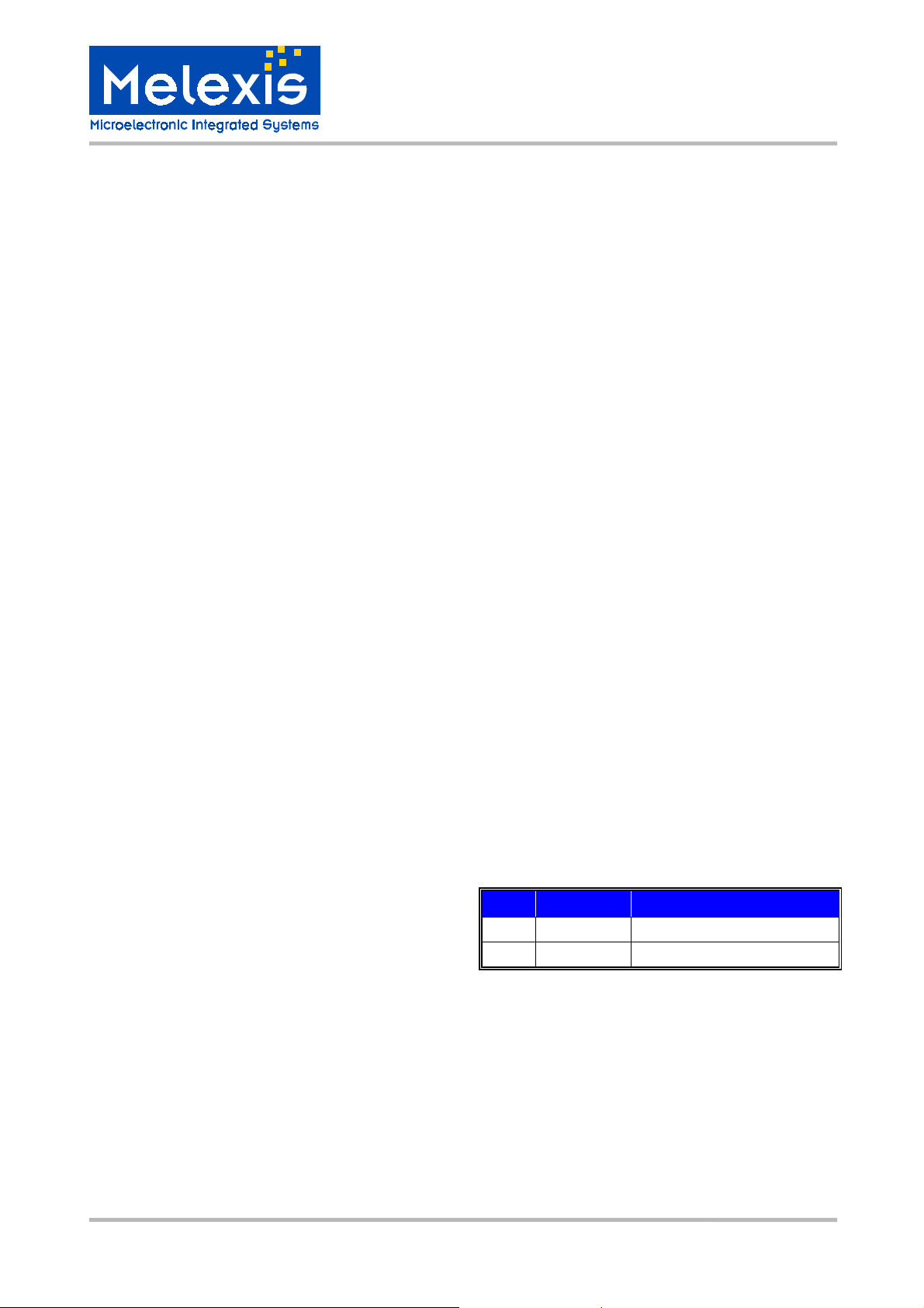
As depicted in Fig.1, the TH71072 transmitter
consists of a fully integrated voltage-controlled
oscillator (VCO), a divide-by-32 divider (div32), a
phase-frequency detector (PFD) and a charge
pump. An external loop filter at pin LF determines
the dynamic behavio ur of the PLL and suppres ses
reference spurious signals.
The VCO’s output signal fee ds the power amplifier
(PA). RF signal power P
steps from P
= –15 dBm to -1 dBm, either by
o
changing the valu e of resistor R
voltage V
at pin PS/DATA. The open-collector
PS
output (OUT) can be used to either drive a loop
antenna or to feed a single-ended load impedanc e.
This could be, for example
or a 50Ω output port. In any case, an impedance
matching network should be added in order to
achieve maximum available RF power.
Bandgap biasing ensures stab le operation of the IC
at a power supply range of 2.2 V to 5.5 V.
Clock Output
The TH71072 feature a clock output (CKOUT) that
can be used to drive a µC. The frequency at
CKOUT is f
/4. The clock output is sle w-rate l imited
ref
in order to keep sp urious signal em ission as low as
possible. The voltag e swing at CKOUT depends on
the capacitive loading at this pin.
It is approximate 2 V
can be adjusted in six
o
or by varying the
1
λ
/4 monopol antenna
pp
at C
load
= 5 pF
The transmitter's c arrier frequency f
by the frequency of the reference crystal f
is determined
c
that is
ref
used. The integrated P LL synthesizer ensur es that
each RF value, ranging fr om 310 MHz to 4 50 MHz,
can be achieved by using a cr ystal with reference
frequency accordin g to: f
= fc/N, where N = 32 is
ref
the PLL feedback divider ratio.
ASK Modulation
The TH71072 can be ASK-modulated by applying
data directly at pin PS. This turns the PA on and off
and therefore leads to an ASK signal at the output.
LO Source
Many applications require a stable RF source. For
this purpose, the TH71072 can be used without
modulation as an easy-to-use, PLL-stabilized,
continuous wave (CW) generator.
Frequency Modulation (FM)
For FM operation an external varactor is required. It
simply acts as a pulling capacitor connected in
series to the crystal. Then the analog modulation
signal, applied through a series resistor, directly
modulates the XOSC.
Mode Control Logic
The mode control logic allows two different modes
of operation as listed in the following table. The
mode control pin ENTX is pulled-down internally.
This guarantees that th e whole circuit is shut down
if this pin is left floating.
ENTX Mode Description
0 TX disabled whole circuit in standby
1 TX enable TX active
Table 1: Modes of operation
3901071072 Page 2 of 10 Data Sheet
Rev. 004 Dec. 2001

Block Diagram
TH71072
315/433MHz
ASK Transmitter / LO Source
7
OUT
VCC
5
PS/DATA
6
VCC
4
PA
div32
div 4
PFD
XOSC
ENTX
3
mode
control
VCO
pump
charge
8 VEE
1
LF
CF1
CF2
RF1
CKOUT
2
RO
XTAL
CX1
Fig. 1: TH71072 block diagram with external components
3901071072 Page 3 of 10 Data Sheet
Rev. 004 Dec. 2001
 Loading...