

MELEXIS TH7107 Datasheet
Features
! Fully integrated, PLL-stabilized VCO
! Flexible frequency range from 310 MHz to 450 MHz
! FSK through crystal pulling allows modulation from
DC to 20 kbit/s
! High FSK deviation possible for wideband data
transmission
! ASK achieved by on/off keying of internal
power amplifier
! FM possible with external varactor
! Wide power supply range from 2.2 V to 5.5 V
! High over-all frequency accuracy
! Very low standby current
TH7107
315/433MHz
FSK/FM/ASK Transmitter
! Adjustable output power range from
-12 dBm to +2 dBm
! Adjustable current consumption from
4.8 mA to 11.5 mA
! FSK deviation and center frequency
independently adjustable
! Differential output well-suited for loop
antenna
! External clock available for µC drive,
down to 1.9 V supply
! ”Clock only” mode
! Conforms to EN 300 220 and similar
standard
Ordering Information
Part No. Temperature Range Package
TH7107 -40 C° to 85 °C SOIC16
Application Examples Pin Description
! Keyless car and central locking
! Low-power telemetry
! Alarm and security systems
! General digital data transmission
! General analog audio signal transmission
LF1
SUB
DAT A
RO2
RO1
ENTX
ENCK
CKOUT
1
2
3
4
TH7107
5
6
7
8
16
15
14
13
12
11
10
9
LF2
VCC
VEE
OUT1
OUT2
VEE
VCC
PS
3901007107 Page 1 of 14 Data Sheet
Rev. 005 Dec. 2001
General Description
TH7107
315/433MHz
FSK/FM/ASK Transmitter
The TH7107 FSK/ASK/FM transmitter IC is
designed for applications in the European 433MHz
industrial-scientific-medical (ISM) band, according
to the EN 300 220 telecommunications standard. It
can also be used for any other system with carrier
frequencies ranging from 310 MHz to 450 MHz
(e.g. for applications in the US 315MHz ISM band).
Theory of Operation
General
As depicted in Fig.1, the TH7107 transmitter
consists of a fully integrated voltage-controlled
oscillator (VCO), a divide-by-32 divider (div32), a
phase-frequency detector (PFD) and a charge
pump. An external loop filter at pin LF determines
the dynamic behavior of the PLL and suppresses
reference spurious signals.
The VCO’s output signal feeds the power amplifier
(PA). RF signal power P
steps from P
= –12 dBm to +2 dBm either by
o
changing the value of resistor R
voltage V
at pin PS. The open-collector differential
PS
output (OUT1, OUT2) can be used to either directly
drive a loop antenna or to be converted to a singleended impedance by means of a balanced-tounbalanced (balun) transformer. For maximum
available output power, the differential output
should be matched to a load of approx. 1 kΩ.
Bandgap biasing ensures stable operation of the IC
at a power supply range of 2.2 V to 5.5 V.
FSK Modulation
A Colpitts crystal oscillator (XOSC) is used as the
reference oscillator of a phase-locked loop (PLL)
synthesizer. FSK modulation is achieved by pulling
the crystal (XTAL) through the data. So a CMOScompatible data stream applied at input DATA
digitally modulates the XOSC. Two external pulling
capacitors CX1 and CX2 allow the FSK deviation
and center frequency to be adjusted independently.
At DATA = LOW CX2 is connected in parallel to
CX1 leading to the low-frequency component of the
FSK spectrum (f
); while at DATA = HIGH CX2 is
min
deactivated and the XOSC is set to its high
frequency, leading to f
An external reference signal can be directly ACcoupled to pin RO1. Then the TH7107 is used
without an XTAL. The reference signal has to
contain the FSK (or FM) and sets the carrier
frequency.
can be adjusted in six
o
or by varying the
PS
.
max
The transmitter's carrier frequency f
by the frequency of the reference crystal f
is determined
c
that is
ref
used. The integrated PLL synthesizer ensures that
each RF value, ranging from 310 MHz to 450 MHz,
can be achieved by using a crystal with reference
frequency according to: f
= fc/N, where N = 32 is
ref
the PLL feedback divider ratio.
Frequency Modulation (FM)
For FM operation an external varactor is required. It
simply acts as a pulling capacitor connected in
series to the crystal. Then the analog modulation
signal, applied through a series resistor, directly
modulates the XOSC.
ASK Modulation
The TH7107 can be ASK-modulated by applying
data directly at pin PS. This turns the PA on and off
and therefore leads to an ASK signal at the output.
Mode Control Logic
The mode control logic allows four different modes
of operation as listed in the following table. The
mode control pins ENCK and ENTX are pulleddown internally. This guarantees that the whole
circuit is shut down if these pins are left floating.
The clock output CKOUT can be used to drive a µC.
This output can be activated by the ENCK pin as
required for any specific application. Clock
frequency is 1/4 of the reference crystal frequency.
ENCK ENTX Mode Description
0 0 all OFF whole circuit in standby
0 1 TX only TX functionality only, no
clock available
10clock
only
11all ON
TX in standby and clock
available
TX functional and clock
available
Table 1: Modes of operation
3901007107 Page 2 of 14 Data Sheet
Rev. 005 Dec. 2001
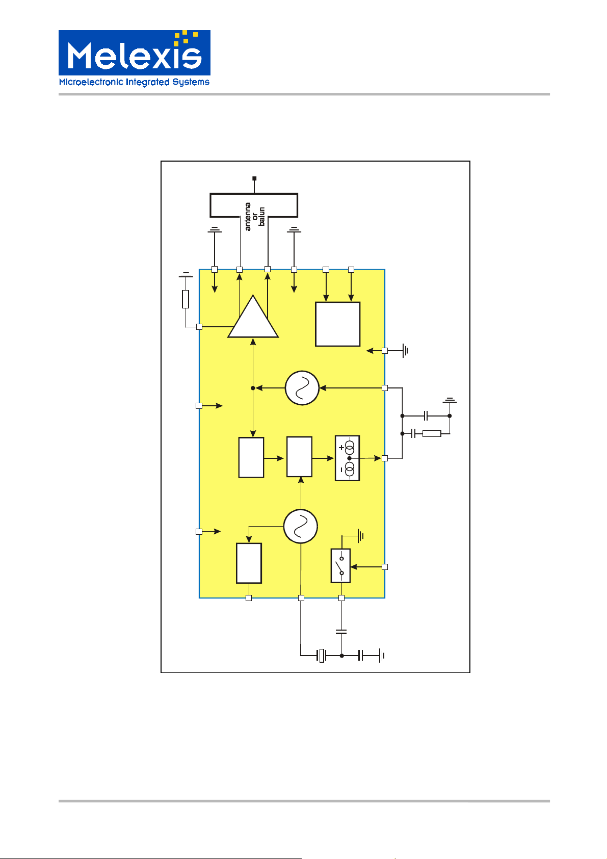
Block Diagram
RPS
VEE
14
OUT1
13
VCC
OUT2
12
VEE
11
ENCK
7
TH7107
315/433MHz
FSK/FM/ASK Transmitter
ENTX
6
PA
div32
XOSC
VCC 10 VCC PS15 9
div 4
8
RO1
CKOUT
VCO
PFD
mode
control
2LF2 SUB
16
pump
charge
1
DATA LF1
3
5
XTAL
4
RO2
CX2
CX1
CF1
CF2
RF1
Fig. 1:TH7107 block diagram with external components
3901007107 Page 3 of 14 Data Sheet
Rev. 005 Dec. 2001
TH7107
315/433MHz
FSK/FM/ASK Transmitter
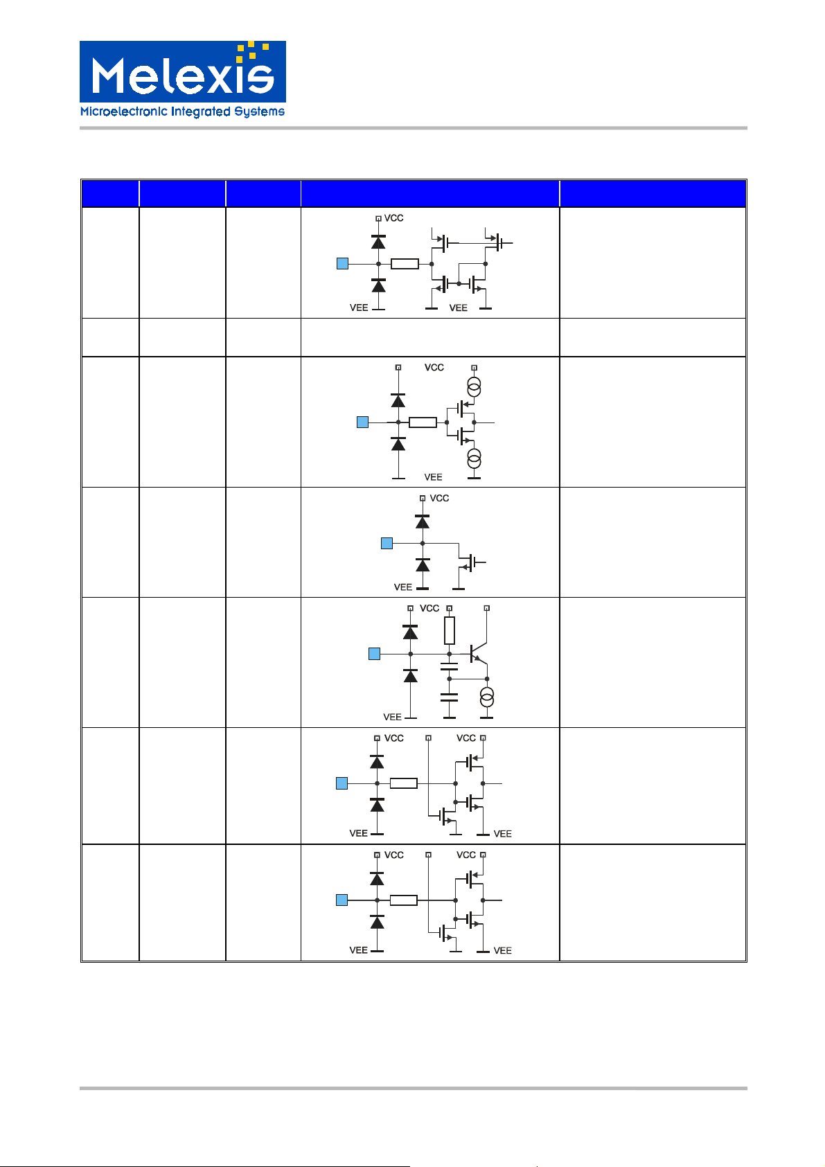
Pin Definition and Descripti on
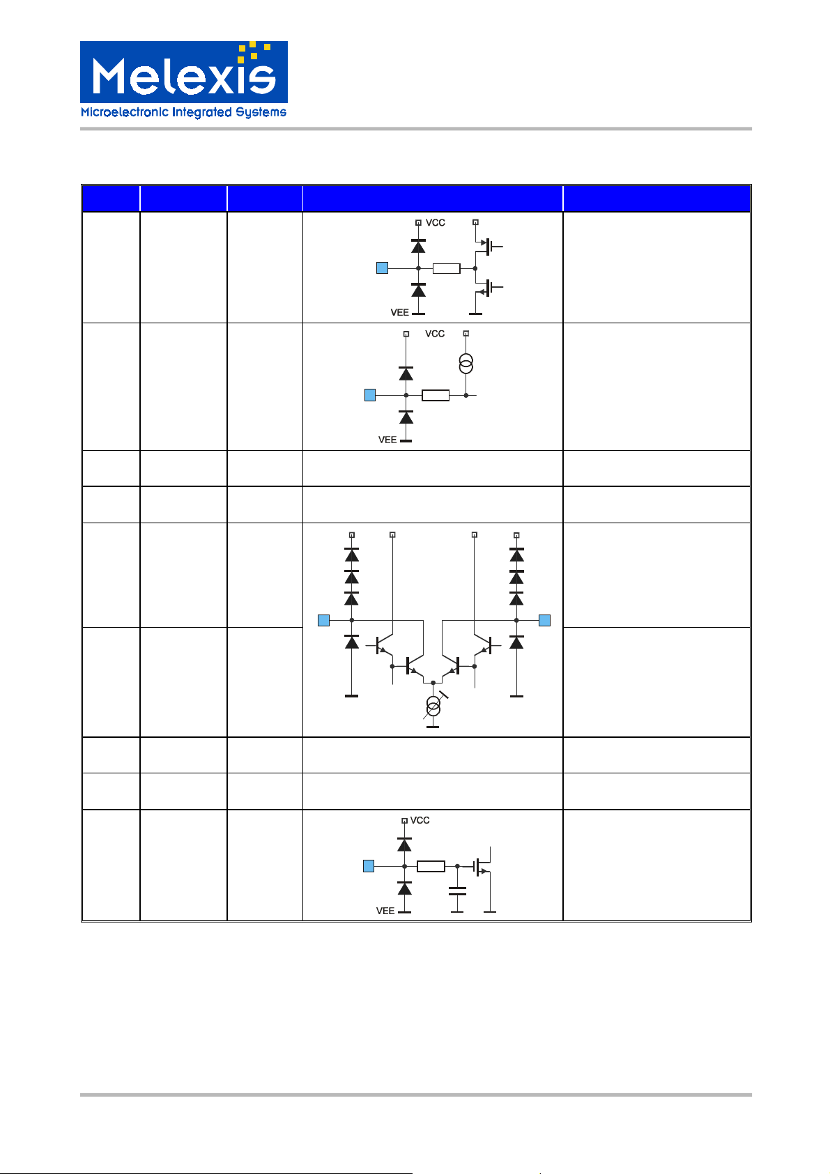
Pin No. Name I/O Type Functional Schematic Description
1 LF1 output
charge pump output,
connection to loop filter
LF1
1
200
Ω
2 SUB ground negative power supply,
substrate connection
3 DATA input
FSK data input,
CMOS-compatible
DATA
3
1.8k
4 RO2 analog I/O
XOSC FSK pulling pin,
MOS switch
RO2
4
5 RO1 analog I/O
RO1
37k
XOSC connection to XTAL,
Colpitts type crystal
oscillator
6 ENTX input
7 ENCK input
ENTX
6
ENCK
7
5
28p
28p
mode control input, CMOScompatible with internal pull-
1.1k
down
mode control input, CMOScompatible with internal pull-
1.1k
down
3901007107 Page 4 of 14 Data Sheet
Rev. 005 Dec. 2001
TH7107
315/433MHz
FSK/FM/ASK Transmitter
Pin No. Name I/O Type Functional Schematic Description
8 CKOUT output
clock output,
CMOS-compatible
CKOUT
8
200
Ω
9 PS analog I/O
power-select and ASK input,
high-impedance comparator
PS
20µA
200
Ω
9
logic
10 VCC supply positive power supply
11 VEE ground negative power supply
12 OUT2 output differential power amplifier
VCC
VCC
output, open collector
OUT2
OUT1
13 OUT1 output
12
13
differential power amplifier
output, open collector
VEE
VEE
VEE
14 VEE ground negative power supply
15 VCC supply positive power supply
16 LF2 input
VCO tuning input,
connection from loop filter
LF2
16
200
Ω
5p
3901007107 Page 5 of 14 Data Sheet
Rev. 005 Dec. 2001
 Loading...