

MELEXIS TH6503 Datasheet
TH6503
USB Low-Speed Interface
Description
Features
TH6503 Sample
Application
The TH6503 is an integrated circuit which enables
the Universal Serial Bus (USB) to be connected to
a microcontroller. The interface module contains
all the components required to transmit data via
the USB.
The TH6503 has been developed for applications
requiring a low speed interface to the USB. Any
microcontroller can be used for control purposes.
In addition to the default endpoint 0 for control
transfer up to two endpoints can be supported by
TH6503. The TH6503 has been developed in
conformity with USB Specifications 1.1.
? Complient with USB Specification 1.1
? Supports up to three programmable endpoints
for interrupt and control transfer in each direction
? Data transfer at USB low speed
? Supports suspend mode
? Universal serial microcontroller interface
? Register programmable
? Programmable 1.5 MHz to 6 MHz out clock for
microcontroller
? Provides power supply for the microcontroller
(3.3 volts or 5 volts)
? Integrated oscillator for clock generation,
supports 6 MHz quartz, ceramic resonator
or external clock input
? Simple external circuitry
TH6503
Interface
to USB
Host / Hub
Figure 1. Typical TH6503 Sample Application
Figure 1 demonstrates a typical TH6503 application. The TH6503 translates the data and control
signals received from the USB in a serial format
which can be read by the microcontroller. The data
is stored in a FIFO buffer and can be called up from
a standard microcontroller via a register programmable serial interface at any time and processed
further. Data generated by peripheries is passed
Rev. 3.5
Dec 2000
USB
Interface
OCLK
/ORST
Serial
Microcontroller/
Customer
Application
to the TH6503 with the same protocol and stored
in a FIFO buffer until it is collected by the USB. The
TH6503 translates all the data in the USB-specific
format and generates the necessary control signals. The TH6503 requires a minimum number of
external elements and can easily be implemented
in a circuitry. It provides an external clock which
can be used to activate a microcontroller.

TH6503 USB Low-Speed Interface
Function USB Data Transmission
The TH6503 supports the USB Specification 1.1
data model.
Data from the USB host to the device and vice
versa is transmitted serially. The data are NRZI
coded to increase transmission reliability; bit
stuffing (inserting an extra 0 bit after any
6 consecutive 1 bits) is performed and a CRC check
carried out. Bit stuffing, NRZI coding/decoding and
CRC checks or generation are performed within the
TH6503.
The data is transmitted in packets. Three types of
packets are defined for the USB: token, data and
handshake.
TH6503/
Microcontroller
Cooperation
to USB
Hub/Host
USB
Interface
TH6503
Interrupt
Transfer
Control
Transfer
Endpoint 2
Endpoint 1
Endpoint 0
The token is always passed on by the host.
It contains a PID (packet identifier) which defines the
direction of the following data transmission and the
address of the device and endpoints to be addressed.
Depending on the previous token command, data is
transferred from the USB host to the TH6503 (OUT
transfer) or transferred from the TH6503 to the USB
host (IN transfer). In the process the respective
FIFOs are written (OUT) or read (IN).
The data transfer is concluded with a handshake.
If the data has been received successfully, an ACK
is sent to the data source. If no data is ready for an
IN transfer out of the TH6503, it sends an NAK
handshake instead of the data (if endpoint is enabled).
serial
Data
Micro-
controller
Vendor specific
Data
Input
Device
Figure 2. Data Flow
The TH6503 is responsible for the data flow between the USB and the microcontroller. It ensures
that the USB transfers the data in line with the
protocol. All information in the protocol layer is
decoded by the TH6503 and carried out accordingly.
The data arriving from the USB host is stored in a
FIFO buffer until it is collected by the microcontroller.
Data transmitted to the USB host are imported
from a FIFO buffer which has previously been filled
by the microcontroller. A /INT signal signals to the
microcontroller that the FIFO status has been
changed by USB.
Data is transferred between the microcontroller
and the TH6503 via a software-emulating serial
interface controlled by the microcontroller.
As the TH6503 cannot interpret the content of the
data, it must be evaluated within the microcontroller.
This also applies to USB-specific control information. All USB-typical descriptors and the associated requests must be created and managed by
the microcontroller.
The setting of the USB address serves here as an
example. After resetting the USB, the address is
set to the default value 0 (USBAddressRegister). A
specific address is transferred from the USB host
software to the device with the SET_ADDRESS
command. This command, like all SET and GET
commands, can only be decoded by the microcontroller. The USB address is decoded in the
TH6503 with the aid of the USB AddressRegister.
For this reason the microcontroller must write the
USB address determined in this register.
The TH6503 supports the USB suspend mode.
Control takes place via the microcontroller. The
ACT bit can be used in the StatusRegister <5>
which is set on the USB for each activity. If this bit
has been inactive for a longer period of time (3 ms),
the microcontroller can set the TH6503 and itself in
the suspend mode using the SUS bit in the
BridgeConfigRegister <4>. The suspend mode
can be ended using the software or an external
signal. Apart from the suspend mode, the TH6503
also supports a number of other power saving
modes which either stop the microcontroller by
switching off the clock or set the whole USB bridge
in a power saving mode.
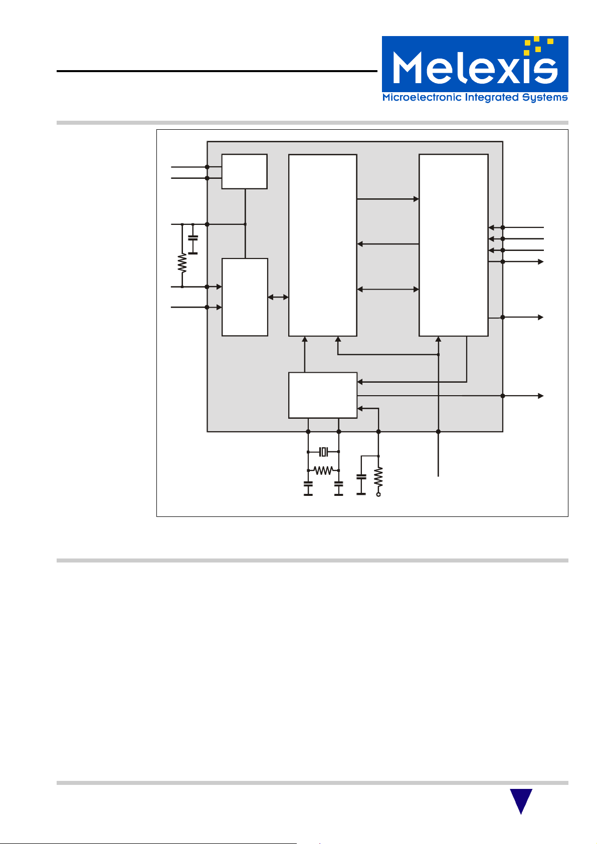
The TH6503 provides the clock pulse for the
microcontroller. It can be programmed with the
OCR 1 - OCR 0 bits in the BridgeConfigRegister
<1-0>.
The TH6503 supplies 3.3V voltage to power the
microcontroller; this is produced by the adjacent
5V bus power supply connection.
2
TH6503 USB Low-Speed Interface
OCLK
SCK
SIN
SDI
SDO
1312111015816
Power
14
/ORST
Micro-
controller
TH6503/
Microcontroller
Cooperation
(continued)
VBus
GND
V3.3
D-
D+
1k5
10µ
1
5
Supply
3.3V
SIE
2
Serial
Interface
Engine
3
4
USB
I/O
Status Signals
Control Signals
Interface
Bus Interface
Microcontroller
Interface
Oscillator/
Divider
6
Figure 3. TH6503 Block Diagram
The data is transferred between the microcontroller and the USB bridge using the clock (SCK)
generated by the microcontroller asynchronous to the USB clock.
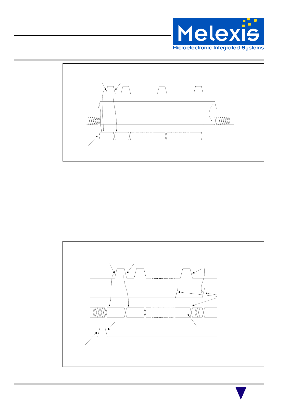
Data IN Transfer
(from the microcontroller to the TH6503)
Data IN transfer is initiated with rising SIN edge (IN
packet sync). Data is transferred via the SDI pin.
Initially the Adr/CntInRegister which indicates the
internal address in the TH6503 is written. Data is
subsequently transferred beginning with byte 0 to
Byte n LSB first. Bits IC3-IC0 in the Adr/CntInRegister
<3-0> contain the information on the number of
bytes to be transferred to the USB host if the target
of the data transfer was an IN FIFO.
A zero data transfer is identified with reset of IC3IC0 bits after writing the Adr/CntInRegister one
additional clock on SCK must be generated.
7
WAKE
RESET
V3.3
If a register is the target of the data IN transfer the
bits IC3-IC0 and TI have no meaning.
With falling SCK edge the microcontroller transmit the bits to SDI and the bits are imported from
the bridge with increasing SCK edge. After each
transmission of 8 bits the respective IN FIFO value
is increased by 1. If the microcontroller writes
more data than indicated in the Adr/CntInRegister,
the oldest data are overwritten. After the final
falling edge of SCK first SDI and then SIN must be
reset to 0 to terminate the transfer. The associated
IN Done bit in the StatusRegister is reset automatically to enable USB IN transfer.
3
TH6503 USB Low-Speed Interface
Microcontroller
Interface
(continued)
SCK
SIN
SDO
Figure 4. Serial Data IN
Bridge latches
Data on rising
edge of SCK
1
0
1
0
1
0
1
SDI
0
Microcontroller outputs
Adr/CntInRegister Bit 0 / AC0
on SDI
Microcontroller shifts
Data on falling
edge of SCK
0 1 7 n+8
End of IN Transfer
/INT
AC7 Data Bit 0 Bit nAC0 AC1 AC2
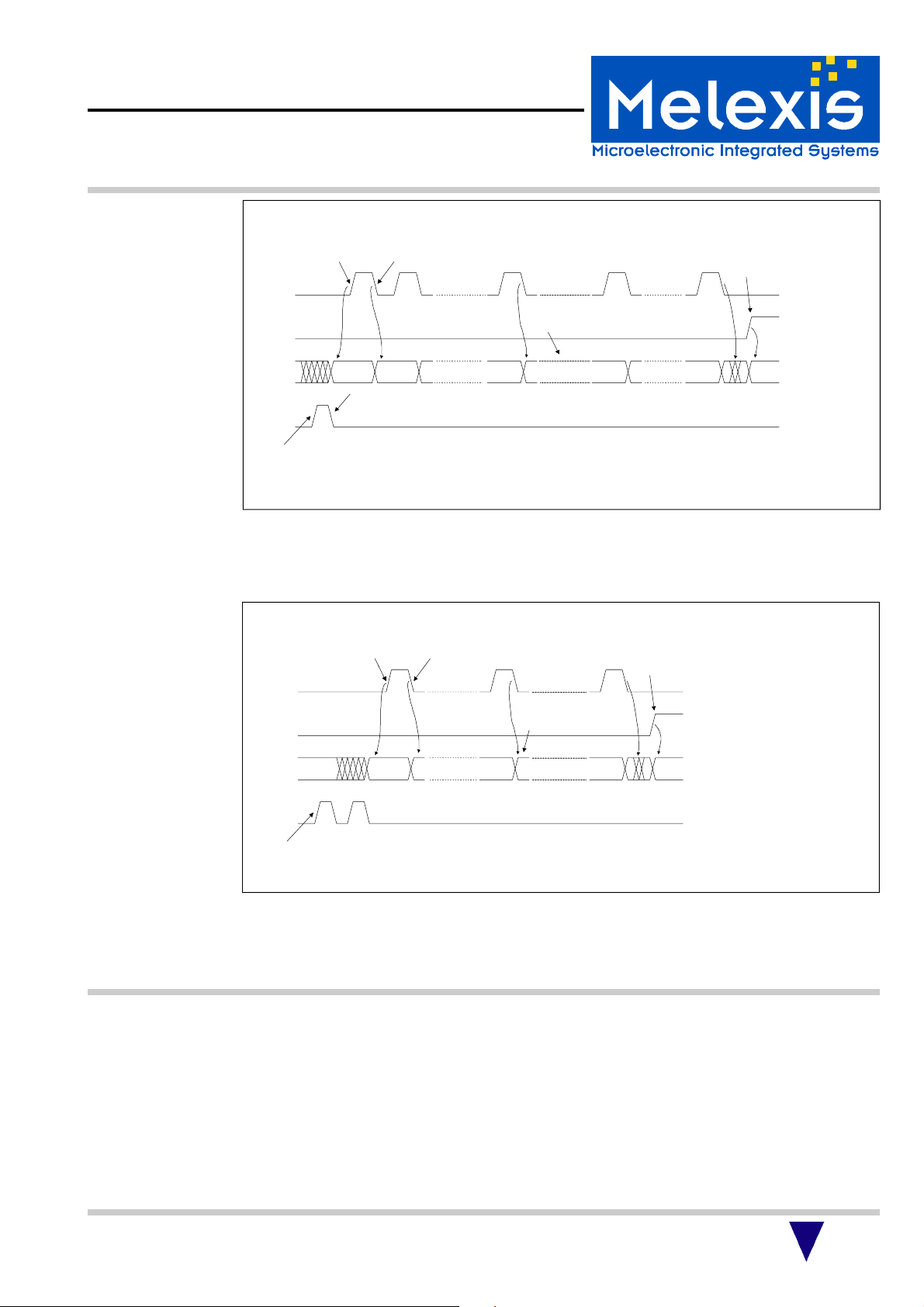
Data OUT Transfer
(from the TH6503 to the microcontroller)
An impulse on the SDI link at SIN = 0 represents
the OUT packet sync for an OUT transfer. With the
falling SCK edge the data (LSB first) is shifted to
SDO and with rising SCK edge accepted by the
microcontroller. The StatusRegister is transferred
initially followed by the CntOutRegister and finally
the OUT FIFO data. If the transfer is terminated after
less than 8 clock pulses, only single StatusRegister
bits are read. Linear transfer is interrupted by SIN
Bridge shifts
Data on falling
edge of SCK
0 1 n
Clear Interrupt Latch
SCK
SIN
SDO
SDI
1
0
1
0
1
0
1
0
Microcontroller
latches Data
on rising edge
of SCK
Status0 Status1 Status2 Status n /INT
= 1 and must be initiated with a new OUT packet
sync at SIN = 0. Two impulses on the SDI link
initiate a transfer of the CntOutRegisters and of the
following OUT FIFO bytes without the
StatusRegister. A zero data transfer is identified by
an OUT Count Byte value of 0. The end of a Data
OUT transfer clears the SET bit in the
CntOutRegister and the OD bit in the
StatusRegister to make the next USB OUT or
Setup transfer possible.
End of
Transfer
any break
after identify the
/INT source possible
n <= 7
SDI pulse with SIN=0:
- copy StatusRegister to Shift Register for Serial Data Out
Figure 5. OUT Transfer of StatusRegister
4
TH6503 USB Low-Speed Interface
Microcontroller
Interface
(continued)
Microcontroller
latches Data
on rising edge
of SCK
1
SCK
0
1
SIN
0
1
SDO
0
1
SDI
0
SDI pulse with SIN=0:
- transfer StatusRegister to Serial Data Out
Figure 6. Complete Data OUT Transfer
Bridge shifts
Data on falling
edge of SCK
0 1 7 15 n+16
Status0 Status1 Status2 Status7 CNT0 CNT7 FIFO Bit 0 Bit n /INT
Clear Interrupt Latch
Bridge outputs
next Register (CntOutRegister)
Bit 0 on SDO
End of OUT Transfer
(OUT Tranfer after reading
the Status -and CntOutRegister
with SIN=0 clears
EP0 Out Done
Interrupt Function
Microcontroller
latches Data
on rising edge
of SCK
1
SCK
0
1
SIN
0
1
SDO
0
1
SDI
0
Two SDI pulses with SIN=0:
- transfer CntOutRegister and OUT FIFO Bytes
to Serial Data Out
Bridge shifts
Data on falling
edge of SCK
0 7 n+8
Bridge outputs
next Register (FIFO)
Bit 0 on SDO
CNT0 CNT1 CNT7 FIFO Bit 0 Bit n /INT
End of OUT Transfer
(OUT Tranfer > 8 clocks
the Status -and CntOutRegister
with SIN=0 clears
EP0 Out Done
Figure 7. OUT Transfer, only CntOutRegister and OUT FIFO Bytes
If SIN = 1, the SDO pin can be used to generate an
interrupt signal. The interrupt is low active. It is
triggered if a control transfer is made from the USB
host or a control or interrupt transfer is made to the
USB host and one of the ID12, ID0 or OD bits has
been set in the StatusRegister <3-1> or at high
level of the WAKE pin. An interrupt signal is also
triggered on RESUME and USB_RESET.
The interrupt latch is reset on reading the status
register. If an interrupt is generated during reading StatusRegister, this interrupt is latched and
the interrupt source is after new StatusRegister
reading visible.
A WAKE interrupt is only generated during the stop
state (bits SO and/or SMC in the BridgeConfig
Register are set).
5
TH6503 USB Low-Speed Interface
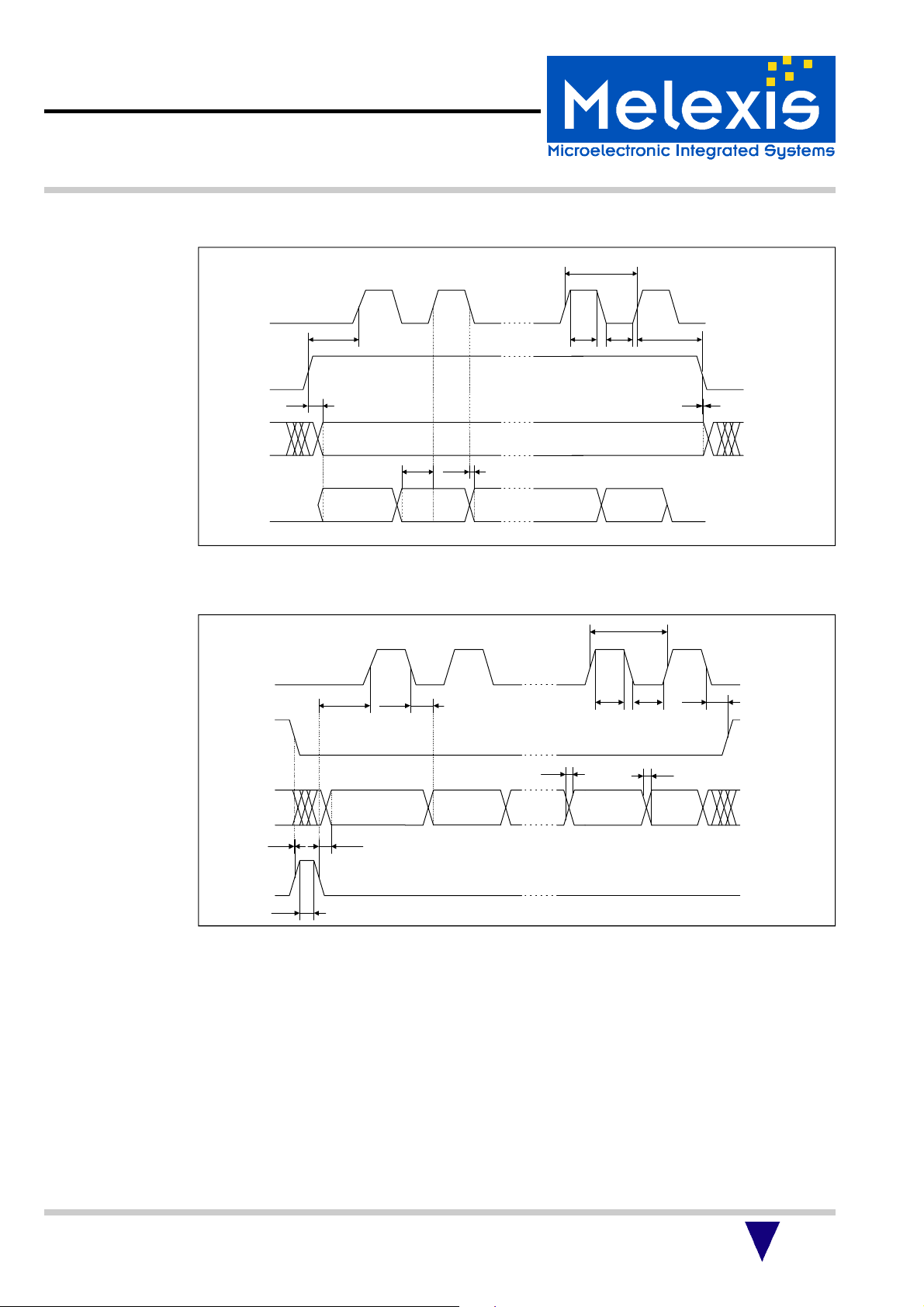
Timing Serial
Interface
Figure 8 and Figure 9 show the timing of the serial interface of the TH6503. The serial interface is
controlled by a standard microcontroller. It can be connected with any microcontroller port.
t
3
SCK
t
t
6
t
4
t
5
7
SIN
SDO
SDI
t
8
/INT
t
10t11
Bit 0 Bit n
t
9
Figure 8. Timing Serial Data IN
t
3
SCK
t
t
16
17
SIN
SDO
t
12
Bit 0 Bit n
t
15
SDI
t
14
Figure 9. Timing Serial Data OUT
t
t
4
t
1
t
5
13
t
2
6
TH6503 USB Low-Speed Interface
Timing Serial
Interface
(continued)
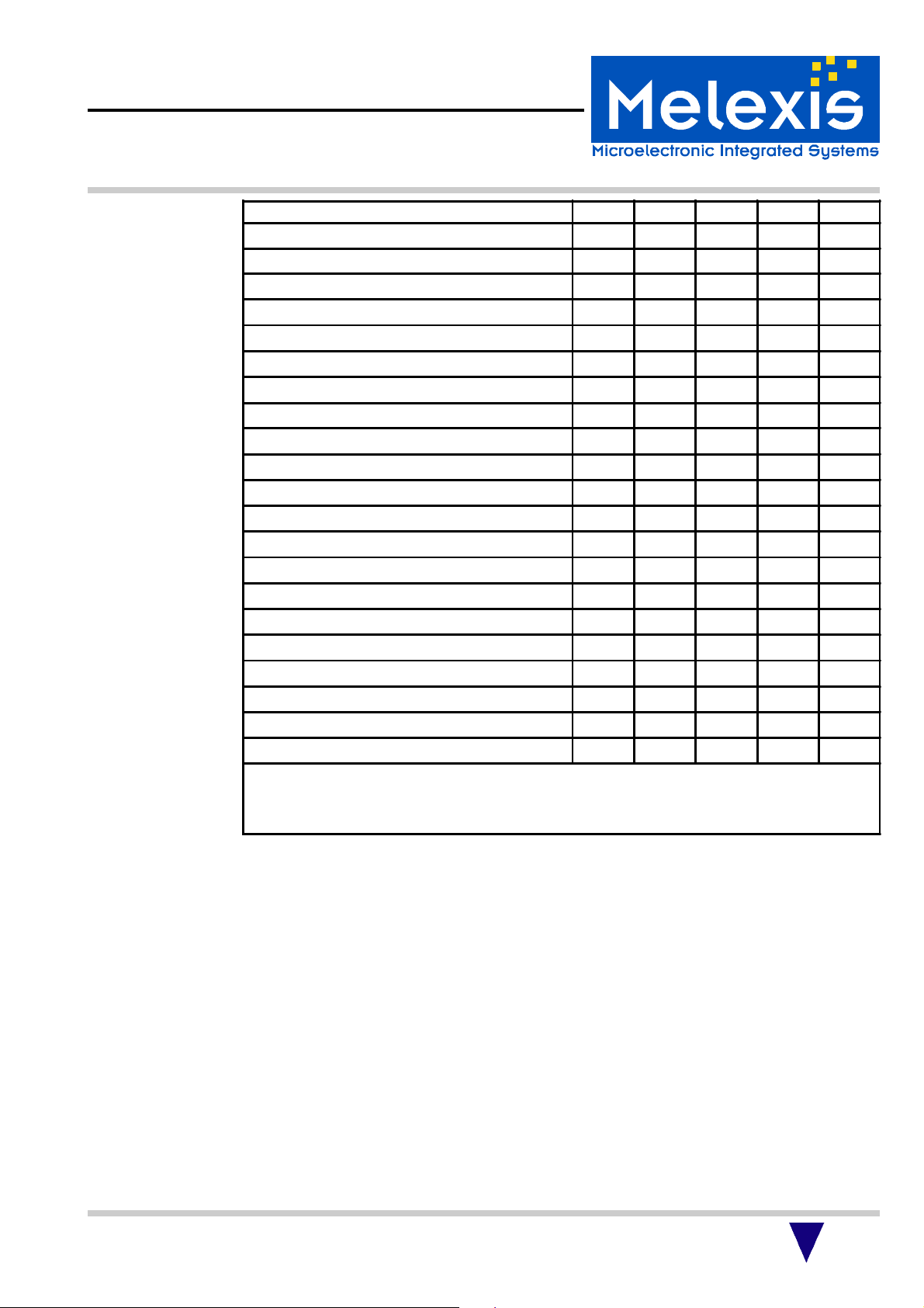
Description [1] Symbol Unit min typ max
General
Oscillator Input period on OSC1 ns 164 170
Rising time of SDO t
Falling time of SDO t
SCK period t
High time SCK [2] t
Low time SCK [2, 3] t
1
2
3
4
5
ns 20
ns 7
ns 600 Step
ns 345
ns 255
Data IN
Setup time of SCK after rising edge of SIN t
Hold time of SIN after last rising edge of SCK t
Setup time of INT-Signal after rising edge of SIN t
Hold time of INT-Signal after falling edge of SIN t
Setup time of Data on SDI before rising edge of SCK t
Hold time of Data on SDI after falling edge of SCK t
6
7
8
9
10
11
ns 170
ns 170
ns 200
ns 165
ns 170
ns 0
Data OUT
Setup time of SDI-pulse after falling edge of SIN t
Setup time of SIN after last falling edge of SCK t
High time of SDI-pulse t
Setup time of Data on SDO after falling edge of SDI-pulse t
Setup time of SCK after falling edge of SDI-pulse t
Setup time of Data on SDO after falling edge of SCK t
12
13
14
15
16
17
ns 170
ns 170
ns 255
ns 280
ns 170
ns 365
Notes:
[1] Capacitive load of 50 pF
[2] Can be asymmetrical
[3] The low time of SCK between the last bit of a byte and the first bit of the next byte must be at least 510 ns.
Input signals are double buffered and digital filtered. Therefore all spikes with a width < 255 ns are
suppressed.
7

TH6503 USB Low-Speed Interface
Connecting the
TH6503 with a
Microcontroller
The TH6503 can be connected with any microcontroller via a serial interface. The serial outputs
can be connected with any microcontroller ports.
The TH6503 out clock can be used to provide the
clock pulse supply to the microcontroller. The
TH6503
SCK
SIN
SDI
SDO
OCLK
13
12
11
10
15
MC6805
PA0
PA1
PA2
PA3
XOSC1
XOSC2
/ORST
Figure 10. The Connection between the
14
V
3.3
TH6503 and the
MC6805 by Motorola
/RESET
reset output is low active and configured in an
open drain structure. For this reason the output
must be set at a defined level with external V
resistance.
TH6503
SCK
SIN
SDI
SDO
OCLK
13
12
11
10
15
Z86Kxx
P24
P25
P26
P27
XTAL1
XTAL2
/ORST
Figure 11. The Connection between the
14
V
3.3
TH6503 and the Z86Kxx by Zilog
/RESET
3.3
TH6503
SCK
SIN
SDI
SDO
OCLK
13
12
11
10
15
80C51
P1.0
P1.1
P1.2
P1.3
XTAL1
XTAL2
/ORST
Figure 12. The Connection between the
14
V
3.3
TH6503 and the 80C51 by Intel
RST
TH6503
SCK
SIN
SDI
SDO
OCLK
13
12
11
10
15
PIC16C5x
RA0
RA1
RA2
RA3
OSC1
OSC2
/ORST
Figure 13. The Connection between the
14
V
3.3
TH6503 and the
PIC16C54 by Microchip
/MCLR
8
 Loading...