

MELEXIS TH3122 Datasheet

TH3122
K-Bus Transceiver with integrated Voltage Regulator
Features and Benefits
Pin Diagram
SOIC16
K-Bus Transceiver:
PNP-open emitter driver with slew rate control and current limitation
BUS input voltage -24V ... 30V (independently of V
)
S
ISO 9141 and ODBII compliant
Possibility of BUS wake up
Operating voltage V
= 5.5 ... 16 V
S
Very low standby current consumption <100 µA
in normal mode (< 50 µA in sleep mode)
Linear low drop voltage regulator:
Output voltage 5V± 2%
Output current max. 100mA
Output current limitation
Overtemperature shutdown
Configurable reset time (15ms/100ms) and reset threshold voltage (3.15V / 4.65V)
Low voltage detection at VS
Wake-up by K-BUS traffic and start-up capable independent of EN voltage level
VS VCC
EN SENSE
VTR
GND
GND
BUS
SI
SO
1
2
3
4
5
6
7
TH3122
16
15
14
13
12
11
10
98
RESET
GND
GND
TxD
RxD
SEN/STA
Universal comparator with an input voltage range –24V … 30V
and digital output
Load dump protected (40V)
Ordering Information
Part No. Temperature Range Package
TH3122 -40ºC...125ºC SOIC16, 300mil
General Description
The TH3122 consists a low drop voltage regulator
5V/100mA and a K-Bus transceiver. The transceiver is suitable for K-Bus systems conform to
ISO 9141.
The combination of voltage regulator and bus
transceiver in combination with the monitoring
functions make it possible to develop simple, but
powerful and cheap nodes in K-Bus systems.
The wide output current area and the configurable
reset time and reset voltage works together with
many different microcontrollers.
www.melexis.com Page 1 Datasheet Rev 1.0 July 2001
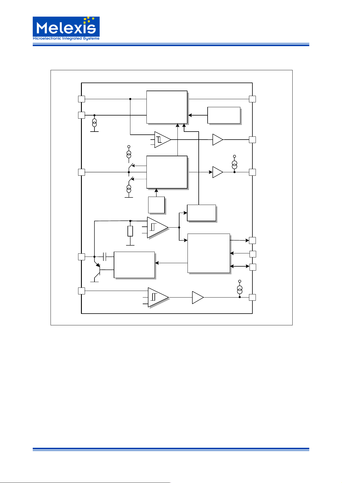
Functional Diagram
TH3122
K-Bus Transceiver with integrated Voltage Regulator
VS
EN
VTR
BUS
7.8V
+5V
6.8V
V
thH
V
thL
pnp Control
slew
rate
foldback
Power Supply
Reset-Logic
VTR-Logic
OSC
Wake-up
Bus-Logic
VCC
Over Temp
SENSE
+5V
RESET
RxD
TxD
SEN/STA
+5V
SI
V
THSI_H
V
THSI_L
Figure 1 - Block Diagram
SO
www.melexis.com Page 2 Datasheet Rev 1.0 July 2001
K-Bus Transceiver with integrated Voltage Regulator
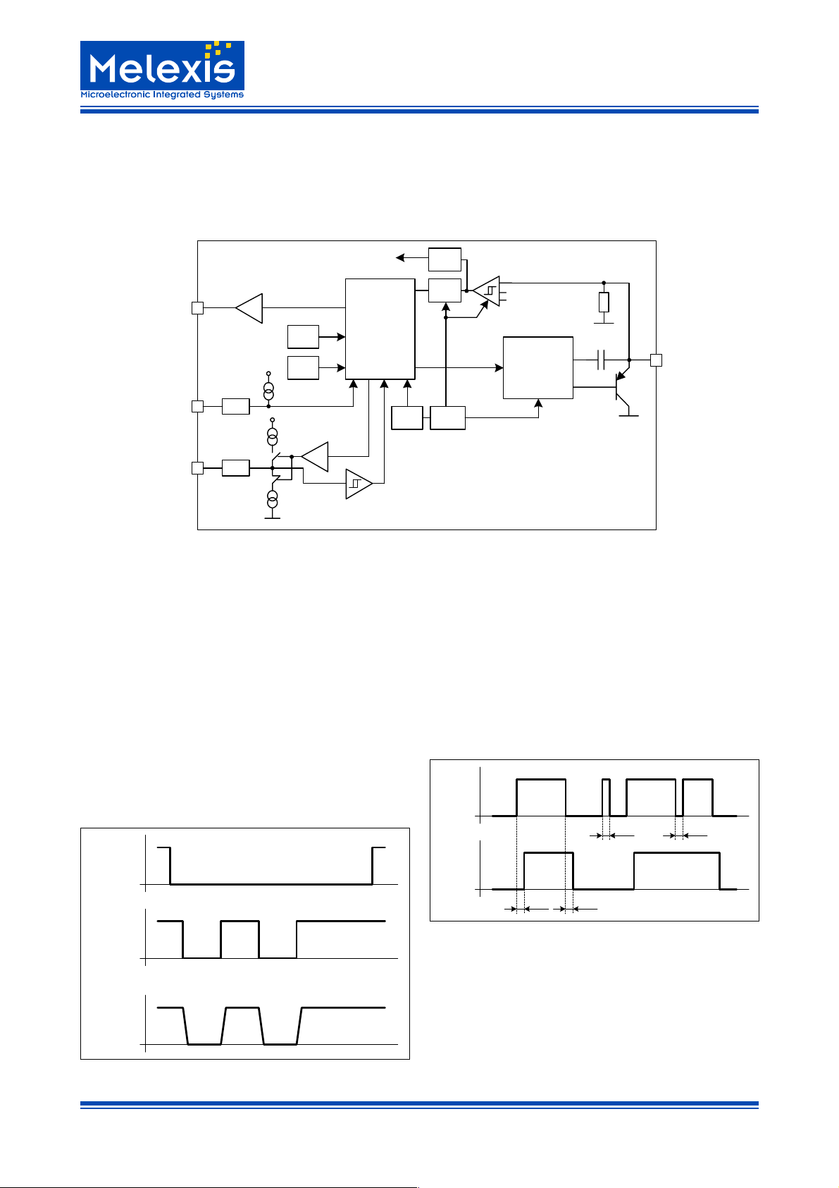
Functional Description
The TH3122 consists a voltage regulator 5V/100mA and
a K-Bus transceiver, which is a bi-directional bus interface device for data transfer between K-Bus and the KBus protocol controller.
TH3122
Also integrated into the transceiver are a voltage and
time controlled reset management, power down, wake
up function and a universal comparator for extended applications.
to Wake-up
Logic
RxD
Control-
logic
POR
TxD
SENSE
ESD
ESD
VCC
VCC
VBAT
POR
VCC
Bit-Compare
Constant-Low
Figure 2 - Block Diagram K-Bus Transceiver
K-BUS Interface
The BUS Interface builds the connection between the serial 5V bus line of the protocol controller and the 12V KBus line.
The transceiver consists a pnp-driver with slew rate control and fold-back characteristic and consists as well in
the receiver a high voltage comparator followed by a debouncing unit.
Transmit Mode
During the transmission the data at the pin TxD will be
transferred to the pin BUS. To minimize the electromag-
SEN/STA
t
debWake
OSC
t
debBUS
Vref
Biasing
V
thH
V
thL
pnp Control
- slew rate
- I
B
- foldback
BUS
netic emission of the bus line, the TH3122 has an integrated slew rate control.
Receive Mode
The data at the pin BUS will be transferred to the pin
RxD. Short spikes on the bus signal are suppressed by
the implemented debouncing circuit.
BUS
< t
debH
RxD
< t
debL
TxD
BUS
Figure 3 - Transmit Mode Pulse Diagram
t
debH
t
debL
Figure 4 - Receive Mode Pulse Diagram
www.melexis.com Page 3 Datasheet Rev 1.0 July 2001
TH3122
K-Bus Transceiver with integrated Voltage Regulator
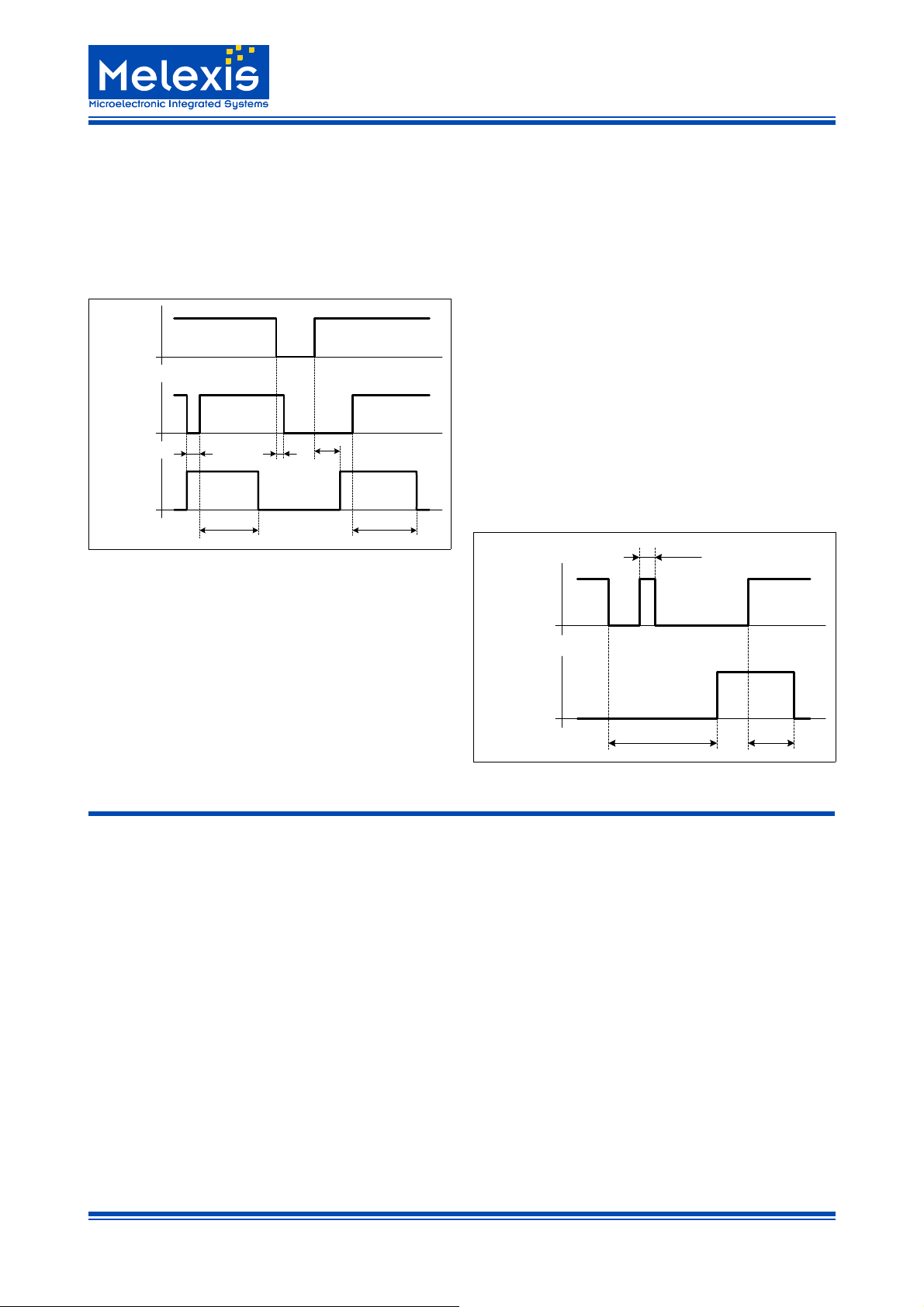
Bit Compare
Are the signals at the pin TxD and the pin BUS
within a specified time t
not identical, the
bc
transmission will be interrupted.
If both signals at TxD and BUS are “High” within
the time t
the transmission will be enabled. The
ena
bit-compare-function is activ when the pin SEN/
STA is open (not overwritten).
BUS
RxD
t
t < t
bc
SEN/STA
t
ena
Figure 5 - Bit Compare Pulse Diagram
bc
t
ena
Using this pin as an input the transmission path
can be overwritten (independent of bit-compare
and constant-low function):
SEN/STA=”0”
forcing the transmission path free
SEN/STA=”1”
disable the transmission path
Constant Low Switch Off
A falling edge at pin TxD (from “1” to “0”) starts the
internal constant low timer (SEN/STA open).
If the low level “0” is valid for the time t
low
the
transmission unit of the TH3122 will be disabled.
The receive unit is still active. A high level “1” at
TxD with a minimum pulse width of t
reset the
rec
constant low timer.
Transmitting is possible not until TxD and BUS is
High for the time t
ena
.
t < t
rec
SEN/STA
The pin SEN/STA is bidirectional. Used as an
output the pin indicates whether the transmit-path
is enabled or disabled:
SEN/STA =”0”
transmission path is enabled
SEN/STA =”1”
transmission path is disabled
Linear Regulator and Controlling Functions
Regulator
The TH3122 has an integrated linear regulator with an
output voltage of 5V ±2% and an output current of max.
100mA. The regulator is switched on or off with a signal
on the EN pin or wake up with a BUS signal.
Initialization
The initialization is started if the power supply is switched
on, or after the temperature limitation has switched off
the regulator or in case of BUS traffic (wake up).
If the V
time t
voltage level is higher than V
CC
is started. This reset time is determined by the
RES
RESEIN
, the reset
TxD
SEN/STA
t
low
t
ena
Figure 6 - Constant Low Pulse Diagram
voltage level on the VTR pin (see table VTR Programming). After t
a rising edge on the RESET output is
RES
generated (see figure 7 - Initialization).
The regulator is active and can only switched off with a
falling edge on EN. The regulator remain with EN=high in
active mode and therefore also the V
voltage is active.
CC
The input EN has an internal pull down resistor. If
EN=high, the internal pull down current is switched off to
minimize the quiescent current.
www.melexis.com Page 4 Datasheet Rev 1.0 July 2001
TH3122
K-Bus Transceiver with integrated Voltage Regulator
VS
V
VCC
RESET
RESEIN
t
Res
V
RES1/2
t
rr
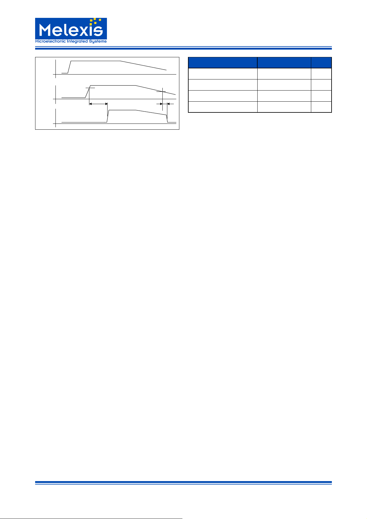
Figure 7 - Initialization
RESET Output
The RESET output is switched from low to high if VS is
switched on and VCC>V
If the voltage VCC drop below V
after the time t
RESEIN
RES1
or V
RES.
then the RESET
RES2
output is switched from high to low after the time trr has been
reached.
The voltage level for V
sponding times t
can be programmed via the ana-
RES
RES1
and V
and the corre-
RES2
logue input VTR.
Wake up with BUS traffic
If the regulator is put in standby mode it can be wake up
with the BUS interface. Every pulse on the BUS (high
pulse or low pulse) with a pulse width of min. 45µs will
switch on the regulator.
After the BUS has wake up the regulator, it can only be
switched off with a high level followed by a low level on
the EN pin.
Reset Programming on VTR
With the VTR pin the reset switch off levels and delay
time can be programmed.
The voltage on VCC influences the reset function.
VTR-Programming
The voltage on VTR input is read out if the voltage at this
pin is higher than V
switch off voltage V
switch on the pull up current source if VTR=low or the
. This value defines the reset
RESEIN
. With the next oscillator cycle it
RES
VTR-Mode V
VTR = GND V
VTR = VCC V
VTR with R ≥ 50kΩ to GND
VTR with R ≥ 50kΩ to VCC
= V
RES
= V
RES
= V
V
RES
= V
V
RES
t
RES
= 3.15V 100ms
RES1
= 4.65V 100ms
RES2
= 3.15V 15ms
RES1
= 4.65V 15ms
RES2
Res
pull down current source if VTR=high. The sources are
active for one oscillator cycle. The level changes during
this procedures on VTR, which depends on the external
pull up or pull down resistors control the reset time t
Res
Temperature Limitation
If the junction temperature 150ºC < Tj < 170ºC the over
temperture recognition will be active and the regulator
voltage and the BUS driver will be switched off. After Tj
fall below 140ºC the TH3122 will be initialized, independently of the voltage levels on EN and BUS.
The function of the TH3122 is possible between T
Amax
and the switch off temperature, but small parameter differences can appear.
Low Voltage Detection VS
Low voltage on VS is monitored on SENSE output.
If V
has reached the level of VS =6.8V then the SENSE
S
output generates low level. The normal
operating range is VS > 7.8V and the SENSE output generates a high level.
Universal Comparator
The TH3122 consist a universal comparator for general
use. The positive input of this comparator is connected to
the pin SI. The input voltage range of SI is 0V...V
input voltage is compared with a fixed reference voltage
at high or low level and the comparator output SO drives
a 5V digital signal.
S.
The
www.melexis.com Page 5 Datasheet Rev 1.0 July 2001
 Loading...