

查询MLX90808LUF-2供应商
Features and Benefits
Absolute Integrated Pressure sensor
Less than 1% error range overall
Programmable through the connector (3 pins)
Trimmable offset and sensitivity
Ratiometric output
Rail-to-Rail output
Output proportional to the applied pressure
Diagnostics of broken supply wires and broken sensor
Output protected against short-circuits at both battery terminals
On-chip Signal Conditioning (single die solution)
Different pressure ranges available
Application Examples
Automotive applications (MAP, T-MAP, HVAC, …)
Industrial applications
Barometric Air Pressure
MLX90808
Absolute Integrated Pressure Sensor
Ordering Information
Part No. Temperature Suffix Package Code Option Description
MLX90808 L (-40°C to 150°C) UF (die on foil) - 2 3 to 7 Bar Pressure Span
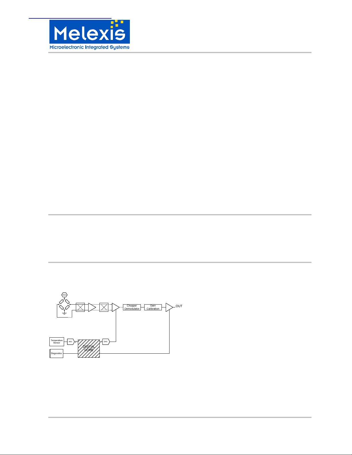
1 Functional Diagram
2
General Description
The MLX90808 is an integrated absolute
pressure sensor realised in CMOS
technology. It consists of an analog signal
chain that interacts with the digital core and
on-chip temperature sensor in order to
provide uniform overall sensing
characteristics after calibration and to cancel
the temperature related parameter drifts.
The output is proportional to the applied
pressure with an adjustable slope and offset.
The chip is ratiometric and goes rail-to-rail
with a 1mA source and sink capability.
3901090808 Page 1 of 8 Data Sheet
Rev 001 Feb 08

MLX90808
Absolute Integrated Pressure Sensor
Table of Contents
1 Functional Diagram........................................................................................................... 1
2 General Description .......................................................................................................... 1
3 Absolute Maximum Ratings .............................................................................................. 3
4 General Electrical Specifications....................................................................................... 3
5 Diagnostic features ........................................................................................................... 4
6 Detailed General Description ............................................................................................ 4
7 Unique Features ............................................................................................................... 5
8 Application Information ..................................................................................................... 5
9 Programming and Calibration ........................................................................................... 6
9.1 Programming of the Temporary Memory of 90808 ..................................................... 6
9.2 Zapping of the 90808 .................................................................................................. 7
10 Disclaimer ....................................................................................................................... 8
3901090808 Page 2 of 8 Data Sheet
Rev 001 Feb 08
Supply current with output shorted to 0V .. 16V
IDD 100 mA
°C
°C
°C
3 Absolute Maximum Ratings
MLX90808
Absolute Integrated Pressure Sensor
Parameter Symb
Min Value Max Value Units
ol
Supply Voltage (overvoltage) VDD -14 16 V
Supply Voltage (operating) VDD 4.5 5.5 V
Supply Current, I
Output Voltage, V
with V
DD
out
= 16 V IDD 25 mA
DD
V
-0.5 16 V
out
Supply Current limit, reverse polarity IDD 160 mA
Programming Temperature Range (ZAP cells) TP -20 100
Operating Temperature Range TA -40 140
Storage Temperature Range TS - 50 150
ESD Sensitivity (AEC Q100 002) -2 2 kV
Table 1: Absolute maximum ratings
Exceeding the absolute maximum ratings may cause permanent damage. Exposure to absolute-maximumrated conditions for extended periods may affect device reliability.
4 General Electrical Specifications
DC Operating Parameters TA = -40 oC to 140 oC, VDD = 5V (unless otherwise specified)
Parameter Symbol Test Conditions Min Typ Max Units
Supply Voltage Vdd Operating 4.5 5 5.5 V
V
Supply Current Idd
Output Current Capability I
output @ low pressure V
output @ full scale pressure V
Low Clamping level V
High Clamping level V
Linearity error V
Ratiometricity error V
Programming Supply V
Zapping Supply V
Zapping Temperature T
out
out
out
6.5 8.5 % Vod
out
91 93.5 % Vod
out
-0.5 0.5 % Vod
out
-0.3 0.3 % Vod
out
10 10.5 V
cc prog
15.5 16 V
zap
- 20 100
zap
Lifetime 15 Year
Power-up time
Power-up time
Response time 0% / 63% Trp 1 ms
Response time 10% / 90% T
rp 10 – 90
Stabilization time Ts 3 ms
Pressure accuracy 1 % FS
Table 2: Electrical specifications
3901090808 Page 3 of 8 Data Sheet
Rev 001 Feb 08
= 5 V ± 10% , excluding output current
dd
V
= 5 V
dd
V
= 5 V
dd
V
= 5 V
dd
T = 0 oC … 85 oC
T < 0 oC or T > 85 oC
4 7 10 mA
1 mA
0.46 0.5 0.54 V
4.46 4.5 4.54 V
3.5 ms
5 ms
1.5 ms
o
C

MLX90808
Absolute Integrated Pressure Sensor
5 Diagnostic features
DC Operating Parameters TA = -40oC to 140oC, VDD = 5 V (unless otherwise specified)
Parameter Symbol Test Conditions Min Typ Max Units
Output when sensor is broken Sensor broken 2 % Vdd
Output when V
Output when V
Output when V
Output when V
Table 3: Diagnostic features
6 Detailed General Description
This chip integrates a pressure sensor and the associated signal conditioning on the same die. The supply
voltage VDD directly supplies the pressure sensor.
The pressure sensing element consists of a square diaphragm realized in the silicon chip by backside
etching. Due to its small thickness this diaphragm reacts to a pressure difference at both of its side by
cambering. The internal strain increases, in particular at the border of the diaphragm. Here, the piezoresistive elements have been implanted into the silicon diaphragm, which act as transducer.
The piezo-resistive elements react to pressure induced changes of strain by changes in their resistance. Four
resistors are placed at all four borders of the square diaphragm. They are arranged in a Wheatstone-bridge.
A chopped instrumentation stage amplifies the differential output signal of the sensor. The gain of this
amplifier can be adjusted with 3 bits. After the input stage, there is a 3 bit programmable coarse offset which
is followed by a differential to single-ended conversion. The reference voltage for this stage is generated by a
10 bit DAC and varies linearly with temperature in order to perform the offset and offset drift compensation. A
digital hardware multiplier calculates this compensation. The temperature signal, serving as input for this
multiplier, is generated from the ADC of the output signal of the internal temperature sensor.
The chopped signal is demodulated with a switched capacitor stage. The buffered output serves as reference
for a 10 bit DAC to perform the span and span drift compensation. The DAC is controlled by the digital part.
Finally the signal is given out by a class AB rail-to-rail amplifier capable of sourcing and sinking large
currents.
A 3-point temperature and 2-point pressure calibration is required (room temperature, a low temperature and
a high temperature), to achieve an error less than ±1% over the complete pressure and temperature range
(the output error is referred to the output span).
PTC (Programming Through Connector) protocol is used to perform calibration.
The programming of the sensor chip is carried out via the analog connections (i.e. supply, ground, signal out).
No additional pins are necessary for calibration.
The output circuit is protected against short circuit to GND, Vbat (16V) and Vdd.
is broken Pull up > 4k7 4 % Vdd
dd
is broken Pull down 0 % Vdd
dd
is broken Pull down > 10kΩ 96 % Vdd
ss
is broken Pull up 100 % Vdd
ss
3901090808 Page 4 of 8 Data Sheet
Rev 001 Feb 08

MLX90808
Absolute Integrated Pressure Sensor
7 Unique Features
Diagnostic Limits
Diagnostic of broken sensor: The output will be forced to ground (or a very low level) when the sensor
membrane breaks.
Diagnostic of broken wires: The output will be forced to ground (or a very low level) when the supply wire
breaks, even when a pull-up is still connected to the output pin.
The output will be forced to the supply voltage (or a very high level) when the ground wire breaks, even when
a pull-down is still connected to the output pin.
Output Protection
The output is protected against short-circuits at either battery terminals. The output can handle voltages
between -0.5V and 16V (independent of supply voltage).
Memlock Function
The memory consists of ZAP cells. When all calibration parameters are programmed, the chip can be locked.
This to avoid unwanted that data be written into the memory cells.
Once the chip is locked in a normal application, we can not read the zap contents and it is not possible to
unlock afterwards, unless the MOW pin is used. This can be done by apply a supply between 2.5V and 3.5V
on the MOW pin, then we can read back the content of the memory cells and zap another cell if necessary.
Clamping Levels
The user can enable the clamping of the output to ensure that the output can not enter the fault band in
normal application.
8 Application Information
47nF
Very few off-chip components are needed (only 2 decoupling capacitors, not higher than 100 nF).
Only 3 pins are used (Vdd, Vss, Out), see pad layout drawing in paragraph 9.
Calibration and Programming is made through the OUT pin.
3901090808 Page 5 of 8 Data Sheet
Rev 001 Feb 08
47nF

MLX90808
Absolute Integrated Pressure Sensor
9 Programming and Calibration
9.1 Programming of the Temporary Memory of 90808
The temporary memory consists of a shift register of flip flops. It is used to search for the correct calibration
settings. Mode 1 (TC[5:0]=01h) is used for this purpose. Afterwards these settings can be put in the
permanent memory. The programming is done through the connector: you only need the application pins
(supply, ground and output). You can enable the programming by forcing the supply high enough (VCC_T).
You can input the data through the OUT pin. The data is Pulse Width modulated. At the end of the
programming, we keep OUT high until VCC has reached his normal level (VCC_N). Thereafter we disconnect
OUT. It is not necessary to do a power-down before the next settings are programmed.
Timings
3901090808 Page 6 of 8 Data Sheet
Rev 001 Feb 08

MLX90808
Absolute Integrated Pressure Sensor
9.2 Zapping of the 90808
The permanent memory of the 90808 is built with zap cells.
The data output of an unprogrammed zap cell is 0. The data output is 1 when the cell is zapped.
It is not possible to reprogram a zap cell to 0. Only 1 bit can be zapped at a time.
You should use the normal mode (TC[5:0]=00h) and program 1 bit to '1' in the temporary memory.
Afterwards you need to increase the supply voltage (VCC_Z) to be able to zap the bit. The zapping starts
when OUT goes high (OUT_Z). There will flow a high current of approximately 200mA during the zapping.
The memlock-bit should be zapped as last bit, because it disables the programming.
The zap cells can also be read out by using mode 5 (TC[5:0]=05h).
One bit should be set to 1 in the temporary memory.
The supply current should be measured at the normal supply voltage.
A low current (ICC_R0) indicates that the zap cell is not programmed.
A high current (ICC_R1) indicates that the zap cell is programmed.
3901090808 Page 7 of 8 Data Sheet
Rev 001 Feb 08

MLX90808
Absolute Integrated Pressure Sensor
10 Disclaimer
Devices sold by Melexis are covered by the warranty and patent indemnification provisions appearing in its
Term of Sale. Melexis makes no warranty, express, statutory, implied, or by description regarding the
information set forth herein or regarding the freedom of the described devices from patent infringement.
Melexis reserves the right to change specifications and prices at any time and without notice. Therefore, prior
to designing this product into a system, it is necessary to check with Melexis for current information. This
product is intended for use in normal commercial applications. Applications requiring extended temperature
range, unusual environmental requirements, or high reliability applications, such as military, medical lifesupport or life-sustaining equipment are specifically not recommended without additional processing by
Melexis for each application.
The information furnished by Melexis is believed to be correct and accurate. However, Melexis shall not be
liable to recipient or any third party for any damages, including but not limited to personal injury, property
damage, loss of profits, loss of use, interrupt of business or indirect, special incidental or consequential
damages, of any kind, in connection with or arising out of the furnishing, performance or use of the technical
data herein. No obligation or liability to recipient or any third party shall arise or flow out of Melexis’ rendering
of technical or other services.
© 2005 Melexis NV. All rights reserved.
For the latest version of this document, go to our website at
www.melexis.com
Or for additional information contact Melexis Direct:
Europe, Africa, Asia: America:
Phone: +32 1367 0495 Phone: +1 603 223 2362
E-mail: sales_europe@melexis.com E-mail: sales_usa@melexis.com
ISO/TS 16949 and ISO14001 Certified
3901090808 Page 8 of 8 Data Sheet
Rev 001 Feb 08
 Loading...