

查询MLX90601 供应商查询MLX90601 供应商
Features and Benefits
• Remote temperature measurement
• Fully linearized signals
• Analog voltage output, digital PWM output and SPI interface
• Factory calibrated
• Rigid PCB with automotive protection circuitry, or flex circuit board.
• EEPROM ECC
• Open drain relay driver output
Applications
• Automotive climate control
• Toasters, microwave ovens and other applications that require temperature control
• Residential, commercial climate control and occupancy detection
• Industrial temperature transducer and monitoring applications
MLX90601 family
IR thermometer modules
Ordering Information
Suffix
Part No Ta Package Type Description PCB
MLX90601 E ZA BAA 8 bit Analog To –20C /120C, Ta 0C..50C Rigid
MLX90601 E ZA DAA PWM, To –20C /120C, Ta 0C..50C Rigid
MLX90601 E ZA CAA Digital SPI/PWM To –20C/120C, Ta 0C..50C, 5V supply Rigid
MLX90601 K ZA BKA 8 bit Analog To –20C /120C, Ta –20C..85C, 5V supply Flex
MLX90601 K ZA CKA Digital SPI/PWM To –20C/120C, Ta -20C..85C, 5V supply Flex
Notes: Ta ambient operating temperature range
MLX90601EZA-XXX: -40C / +85C
MLX90601KZA-XXX: -40C / +125C
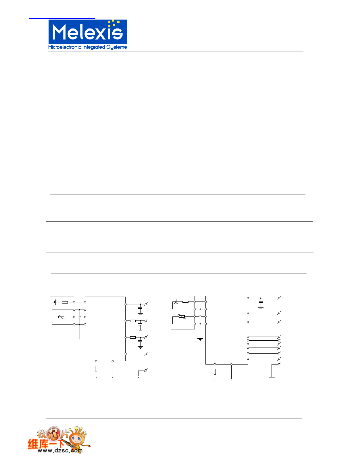
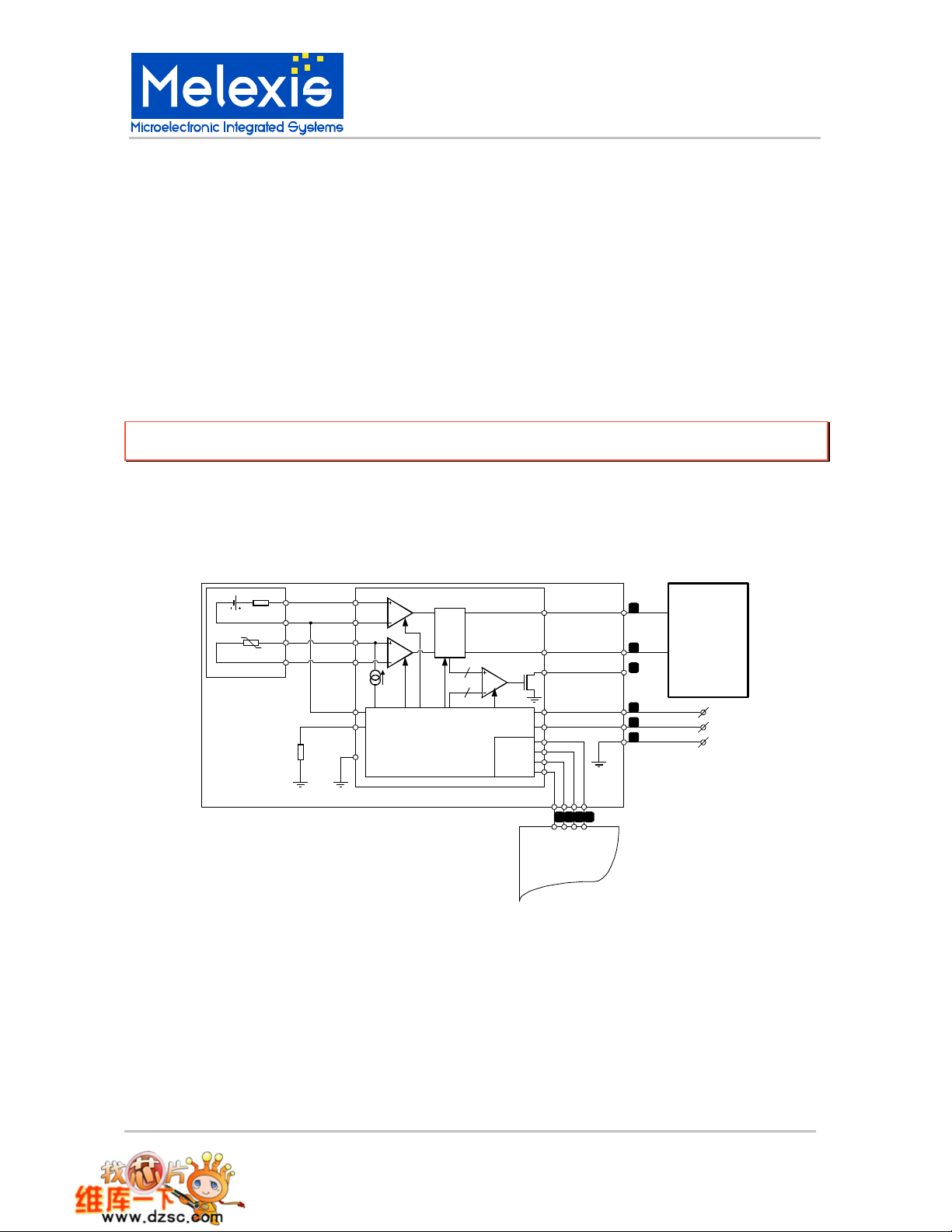
1 Functional Diagrams
MLX90247
Rsens
VSS
VDD
C3
TEMPOUT
IROUT
CS
SCLK
SDI
SDO
REL1 REL
VREFP VREF
MLX90247
Rsens
VSS
IR+
IRINP
IR-
IRINN
TINP
TINN
MLX90313
CREF VSS
R3
IR+
IR-
IRINP
IRINN
TINP
TINN
MLX90313
CREF VSS
R3
VDD
IROUT
TEMPOUT
REL1
R1D
R1C
5V
C3
IROUT
C6
TEMPOUT
C7
REL1
VSS/GND
5V
TEMPOUT
IROUT
CS
SCLK
DIN
DOUT
VSS/GND
MLX90601 EZA-BAA MLX90601 EZA-CAA
MLX90601 EZA-DAA MLX90601 KZA-BKA
MLX90601 KZA-CKA
3901090601 Page 1 of 49 Aug/02
Rev. 007

2 Description
The MLX90601 Family modules are versatile IR
thermometer modules, which perform signal
conditioning, linearisation and ambient
temperature compensation. The modules are
built around the MLX90313 IR sensor interface,
which uses high performance chopper stabilized
amplifiers, providing excellent noise
performance. The sensing element is the
MLX90247 discrete IR thermopile sensor.
The modules are delivered factory calibrated.
The output signals can be analog voltage
outputs; PWM coded digital outputs, or a bidirectional SPI compatible serial interface. All
output signals are linear with the applied
temperature.
All modules feature the open drain relay driver
output available in MLX90313.
Several types of modules are available. First
types are the modules for automotive
applications, which have additional ESD
protection circuitry on board. These modules can
MLX90601 family
IR thermometer modules
have an analog voltage output (MLX90601EZABAA), or a digital PWM coded output
(MLX90601EZA-DAA). The substrate is in this
case a FR4 PCB with a 5 pin through-hole
connector.
Alternatively there are some modules targeted
for industrial or consumer applications. These
modules can have also analog outputs
(MLX90601KZA-BKA) or PWM outputs
(MLX90601KZA-CKA and MLX90601EZA-CAA).
All three modules have a SPI interface available
for full programmability.
The MLX90601KZA-BKA and MLX90601KZACKA are built on a flexible polyamide substrate,
making building in the sensor very easy.
The user can choose now the most suited
module depending on electrical and mechanical
needs.
3901090601 Page 2 of 49 Aug/02
Rev. 007

MLX90601 family
IR thermometer modules
CONTENTS
1 FUNCTIONAL DIAGRAMS ..............................................................................................................1
2 DESCRIPTION................................................................................................................................. 2
3 GLOSSARY OF TERMS ..................................................................................................................5
4 ABSOLUTE MAXIMUM RATINGS...................................................................................................6
5 MLX90601 ELECTRICAL SPECIFICATIONS...................................................................................6
6 GENERAL DESCRIPTION............................................................................................................... 8
6.1 T
6.2 S
6.3 A
7 MLX90601EZA-BAA ...................................................................................................................... 10
7.1 K
7.2 G
7.3 P
7.4 PIN-
7.5 E
7.6 C
7.7 A
8 MLX90601EZA-DAA ...................................................................................................................... 15
8.1 K
8.2 G
8.3 P
8.4 PIN-
8.5 E
8.6 C
8.7 A
9 MLX90601EZA-CAA ...................................................................................................................... 21
9.1 K
9.2 G
9.3 S
9.4 P
9.5 PIN-
9.6 E
9.7 C
9.8 A
10 MLX90601KZA-BKA...................................................................................................................... 30
10.1 K
10.2 G
10.3 S
10.4 P
10.5 PIN-
10.6 E
10.7 C
3901090601 Page 3 of 49 Aug/02
Rev. 007
HEORY OF OPERATION
ENSOR CHARACTERISTICS
CCURACY
EY PROPERTIES
ENERAL DESCRIPTION
HYSICAL OUTLINE
LECTRICAL SPECIFICATIONS
ALIBRATION DETAILS
PPLICATIONS INFORMATION
EY PROPERTIES
ENERAL DESCRIPTION
HYSICAL OUTLINE
LECTRICAL SPECIFICATIONS
ALIBRATION DETAILS
PPLICATIONS INFORMATION
EY PROPERTIES
ENERAL DESCRIPTION
ERIAL PERIPHERAL INTERFACE
HYSICAL OUTLINE
LECTRICAL SPECIFICATIONS
ALIBRATION DETAILS
PPLICATIONS INFORMATION
EY PROPERTIES
ENERAL DESCRIPTION
ERIAL PERIPHERAL INTERFACE
HYSICAL OUTLINE
LECTRICAL SPECIFICATIONS
ALIBRATION DETAILS
.................................................................................................................................. 8
OUT AND PIN DESCRIPTIONS
OUT AND PIN DESCRIPTIONS
OUT AND PIN DESCRIPTIONS
OUT AND PIN DESCRIPTIONS
................................................................................................................ 8
...........................................................................................................8
....................................................................................................................... 10
.............................................................................................................. 10
..................................................................................................................... 12
...................................................................................................... 13
................................................................................................................. 13
....................................................................................................... 14
....................................................................................................................... 15
.............................................................................................................. 15
..................................................................................................................... 17
...................................................................................................... 18
................................................................................................................. 19
....................................................................................................... 20
....................................................................................................................... 21
.............................................................................................................. 21
..................................................................................................................... 26
...................................................................................................... 27
................................................................................................................. 28
....................................................................................................... 29
....................................................................................................................... 30
.............................................................................................................. 30
..................................................................................................................... 35
...................................................................................................... 36
................................................................................................................. 36
.................................................................................................. 12
.................................................................................................. 18
(SPI)......................................................................................... 23
.................................................................................................. 26
(SPI)......................................................................................... 32
.................................................................................................. 35

MLX90601 family
IR thermometer modules
10.8 A
11 MLX90601KZA-CKA...................................................................................................................... 38
11.1 K
11.2 G
11.3 S
11.4 P
11.5 PIN-
11.6 E
11.7 C
11.8 A
12 ESD PRECAUTIONS...................................................................................................................... 46
PPLICATIONS INFORMATION
EY PROPERTIES
ENERAL DESCRIPTION
ERIAL PERIPHERAL INTERFACE
HYSICAL OUTLINE
OUT AND PIN DESCRIPTIONS
LECTRICAL SPECIFICATIONS
ALIBRATION DETAILS
PPLICATIONS INFORMATION
....................................................................................................................... 38
..................................................................................................................... 43
....................................................................................................... 37
.............................................................................................................. 38
...................................................................................................... 44
................................................................................................................. 45
....................................................................................................... 45
(SPI)......................................................................................... 40
.................................................................................................. 43
13 RELIABILITY INFORMATION........................................................................................................ 46
14 FAQ................................................................................................................................................ 46
15 APPENDIX A: SPI INTERFACING TO AUTOMOTIVE MODULES................................................. 48
15.1 C
15.2 SPI C
OMPONENT REFERENCES
OMMUNICATION CABLE PIN-OUT
.......................................................................................................... 48
........................................................................................... 48
3901090601 Page 4 of 49 Aug/02
Rev. 007

3 Glossary of Terms
ADC: Analog to Digital Converter
Ambient Compensation: The IR signal
captured by a thermopile sensor is not only
dependent on the temperature of the object
(Tobject) but also on the temperature of the
sensor itself. Therefore the IR signal is
compensated for this effect by means of the
measured sensor temperature (Tambient). This
rather complex calculation is performed in the
linearisation unit of MLX90313.
Chopper Amplifier: Special amplifier
configuration aimed at ultra low offset.
DAC: Digital to Analog Converter.
EEPROM: Non-volatile memory that can be
electrically erased and rewritten. This type of
memory is used to store configuration and
calibration data for the module.
ECC: Error Checking and Correction. The
EEPROM on board of MLX90313 is equipped
with a checking and correction feature based on
the Hamming Code method.
IR: Infrared. Every object emits infrared
radiation in relation to its temperature. This
effect can be used to measure this temperature
without the need for physical contact.
Linearisation: The signal from a thermopile is
not linear with the object temperature.
MLX90313 is therefore equipped with a digital
calculation unit that produces an output that is
linear with the object temperature.
POR: Power-on reset: Reset circuit that starts
the digital system in a known state whenever the
supply voltage is cycled
PSSR: Power Supply Rejection Ratio: Measure
for an amplifier’s immunity to disturbances on
the supply connections.
PTC: See Thermistor
Ta, Tambient: The temperature of the IR
sensor.
Target: or Object: The object the IR module is
aimed at.
MLX90601 family
IR thermometer modules
Thermistor: Temperature dependant resistor.
Basically there are 2 types. The types that
increase their resistance with rising temperature
are PTC (positive thermal coefficient) type. The
ones that decrease their resistance with rising
temperature we call NTC (negative thermal
coefficient) type. The MLX90313 can work with
both types. The MLX90601 modules are
equipped with sensors that use PTCs.
To, Tobject: The temperature of the object one
wishes to measure with the module
3901090601 Page 5 of 49 Aug/02
Rev. 007
MLX90601 family
IR thermometer modules
4 Absolute Maximum Ratings
Automotive Grade modules
MLX90601EZA-BAA – MLX90601EZA-DAA
Voltage, VDD (over-voltage) 80V
Supply Voltage, VDD (operating) 5.5V
Supply Current, IDD 6mA
Operating Temperature Range, TA
ESD Sensitivity (AEC Q100 002) 4kV
PCB SPI module
MLX90601EZA-CAA
Voltage, VDD (over-voltage) 7V
Supply Voltage, VDD (operating) 5.5V
Supply Current, IDD 6mA
Operating Temperature Range, TA
ESD Sensitivity (AEC Q100 002) 1kV
Exceeding the absolute maximum ratings may cause permanent damage. Exposure to absolutemaximum rated conditions for extended periods may affect device reliability.
-40°C / 105°C
-40°C / 105°C
Flexible modules
MLX90601KZA-CKA – MLX90601KZA-BKA
Voltage, VDD (over-voltage) 7V
Supply Voltage, VDD (operating) 5.5V
Supply Current, IDD 6mA
Operating Temperature Range, TA
ESD Sensitivity (AEC Q100 002) 1kV
-40°C / 125°C
5 MLX90601 Electrical Specifications
DC Operating Parameters TA = -40oC to 125oC, VDD = 4.75V to 5.25V (unless otherwise specified)
Parameter Symbol Test Condition Min Typ Max Unit
Regulator and consumption
POR threshold voltage Vpor 1.1 1.3 1.5 V
IR-chain amplifier and output driver
Power supply rejection
ratio
Input referred white noise Vnir rms-value 25
Chopper frequency fc 8 kHz
Output voltage range IROUT 0 Vdd-0.2 V
Output source current Iod IROUT 1 mA
Output sink current Ios IROUT 20 uA
DC Output impedance,
drive
DC Output impedance,
sink
Amplifier bandwidth BW 500 Hz
Temp-chain amplifier and output driver
Power supply rejection
ratio
Input referred white noise Vntemp rms-value 400
Chopper frequency fc 15 kHz
Output voltage range ORtemp TEMPOUT 0 Vdd-0.2 V
Output source current Iod TEMPOUT 1 mA
Output sink current Ios TEMPOUT 20 uA
PSSR
rod IROUT 10
ros IROUT 100
PSSR
f ≤ 100kHz
f ≤ 100kHz
75 dB
75 dB
nV/√Hz
Ω
Ω
nV/√Hz
3901090601 Page 6 of 49 Aug/02
Rev. 007
MLX90601 family
IR thermometer modules
5 MLX90601 Electrical Specifications
DC Operating Parameters TA = -40oC to 125oC, VDD = 4.75V to 5.25V (unless otherwise specified)
Parameter Symbol Test Condition Min Typ Max Unit
AC Output impedance ro TEMPOUT 100
Amplifier bandwidth BW 500 Hz
Rel1 open drain relay driver
High voltage protections 32 V
output impedance Ro 10
ADC
Monotonic guaranteed by design
Differential non-linearity DNL 0.4 LSB
Integral non-linearity INL ½ LSB
Gain error full scale 1 LSB
Total input-referred noise Vref=3V 0.2 LSB
DAC
Resolution 8 bit
Monotonic guaranteed by design
Differential non-linearity DNL ½ LSB
Integral non-linearity INL ½ LSB
PWM
PWM Clock period Tclk 45 50 55
PWM Total period T 92.16 102.4 112.64 ms
Leading buffer time t1 % of T 12.5
Trailing buffer time t5 % of T 12.5
Duty cycle high t2 % of T 0 50 %
Duty cycle low t3 % of T 0 50 %
Error signal t4 % of T 25
Rise time* 10% to 90% of Vh 13.3 100
Fall time* 90% to 10% of Vh 13.3 100
Output voltage high Vh Ihigh=2mA 4 V
Output voltage low Vl Ilow=2mA 1 V
*Without external loading
Ω
Ω
µs
%
%
%
µs
µs
3901090601 Page 7 of 49 Aug/02
Rev. 007

MLX90601 family
IR thermometer modules
6 General Description
6.1 Theory of operation
The MLX90601 modules are developed especially to make IR temperature sensing easy. All modules
have a linearised output signal. Also they are factory calibrated, so making all modules interchangeable.
Also this relieves customers from complex calibration procedures.
All modules have a MLX90247 thermopile sensor as IR sensing element. The output of this sensor is a
function of both Object (IR) and ambient temperature. Ideally the output voltage of the thermopile sensor
is:
α
Where To is Object temperature in Kelvin, and Ta is the ambient temperature in Kelvin. Alpha is a device
constant. It is clear from above equation that the ambient temperature must be known before the object
temperature can be calculated. Therefore the MLX90247 thermopile sensor has a thermistor built-in.
Melexis has designed a powerful ASIC to perform the signal processing of the thermopile output voltage.
MLX90313 amplifies the signals coming from MLX90247 and converts them to digital by means of two
high performance, low noise, chopper stabilized amplifiers and the 12-bit analog to digital converter. The
digital unit on the interface then performs the ambient compensation of the IR signal. This results in two
temperature signals, one representing the temperature of the object the IR sensor is pointed at (Tobject)
and one representing the temperature of the sensor (Tambient). Both signals are then linearised and
presented at the outputs in analog of PWM coded form. When using modules that have also SPI, the
temperature registers can be read directly through the serial interface.
The linearisation unit can only operate when both Ta (ambient temperature) and To (object temperature)
are both in a distinct calibrated range. This has an important implication for the ambient temperature.
When the modules are used outside the calibrated ambient temperature, the object temperature is
calculated using a false ambient temperature, resulting in an erroneous output signal. If the ambient
temperature is below the ambient calibration range, the OVL flag in the SPI register is set and the
temperature data bits are all zero. For analog output modules, the output will be zero volts. Alternatively, if
the ambient temperature is above the ambient calibration range, the OVH flag in the SPI register is set
and the temperature data bits are all one. For analog output modules, the output will be 4.5 volts.
When returning into calibrated ambient temperature range, the module will resume normal operation.
Our standard products have such ranges that they can suit a maximum number of applications. Currently
there are four different versions of modules offered.
44
)(
TaToVir −=
6.2 Sensor characteristics
All modules have the same thermopile sensor. For detailed specification we refer to the datasheet on
MLX90247, available from the Melexis web site. In a calibrated module the linearisation unit of MLX90313
takes all characteristics of the sensor into account, including all process variations they are subject to.
The TO-39 sensor housing of the thermopile has a 2.5mm diameter aperture, resulting in a 70° full angle
field of view, for 90% % of the IR energy. The silicon filter used as IR-window is treated with an
antireflective coating that will pass minimum 75% of IR radiation in the wave length band from 7.5µm to
13.5µm.. Below 5µm, 99.5% of incoming radiation is reflected by the filter. This makes the sensor
insensitive to visible light.
6.3 Accuracy
Accuracy of the module depends mainly on calibration precision. For absolute accuracy please refer to
calibration details for the appropriate module. The error of the output depends on both object and ambient
temperature. Repeatability and stability are very good, the error is < 0.4C, but both ambient and object
3901090601 Page 8 of 49 Aug/02
Rev. 007

MLX90601 family
IR thermometer modules
temperature must be kept stable. For making relative measurements care must be observed. The
MLX90313 uses a piecewise modified quadratic approximation method, and on the reference points, the
output can change with several tenths of degrees. Of course, the absolute accuracy will always be within
specification.
3901090601 Page 9 of 49 Aug/02
Rev. 007

MLX90601 family
5.4
IR thermometer modules
7 MLX90601EZA-BAA
7.1 Key properties
• Automotive use
• analog output signals with 8 bit resolution
• relay comparator
• only 5 connections
7.2 General description
The MLX90601EZA-BAA is a module that is targeted for automotive use. In addition to the small amount
of components like the sensor, ASIC etc there are also 2 RC protection circuits on the IROUT and
TEMPOUT pins. This allows the module to be used in automotive environments.
The Object temperature information is available at the IROUT pin. The ambient temperature information is
available on the TEMPOUT pin. The resolution of the output D/A converter is 8bit. The output drivers
have a maximum output voltage of 4.5V when the maximum calibrated temperature is reached.
If the ambient temperature is out of the calibrated temperature range, the correct object temperature
cannot be calculated. For applications where the ambient temperature can rise above the maximum
calibrated temperature, the ambient temperature output must be monitored to make sure the object
temperature is valid.
Next to the temperature outputs there is also a relay driver output. The relay driver has a threshold that is
pre-set to 50 °C, with a hysteresis of 5 °C. Note that this module has no SPI interface connector available.
If the user wants to reconfigure this type of module, this can be done with the EVB board and a special
test clip. Refer to appendix A for details.
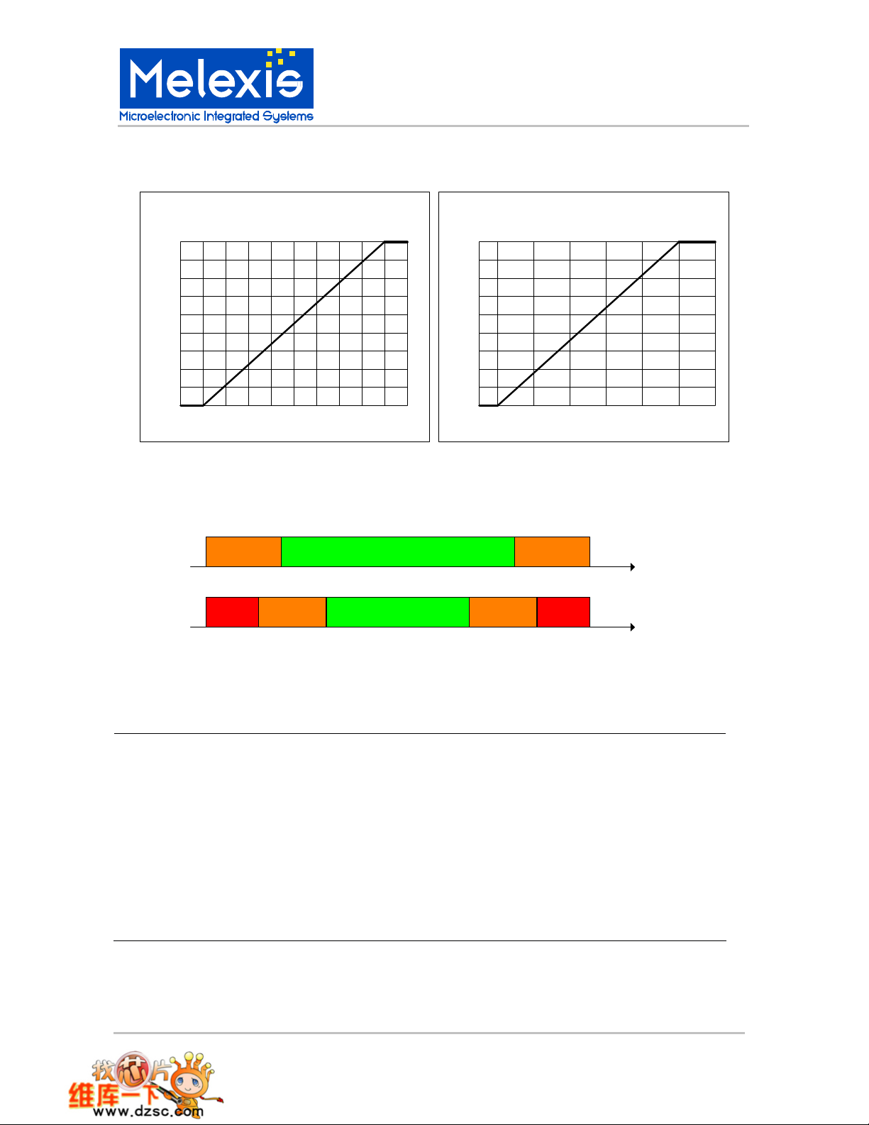
The relation of the output voltage to the temperature is defined as follows:
Vout
T +−= *
( )
TminTminTmax
where:
T measured temperature
Vout analog output voltage on IROUT or TEMPOUT pins.
Tmin minimal calibrated temperature
Tmax maximum calibrated temperature
Refer to calibration details for calibrated ranges info
3901090601 Page 10 of 49 Aug/02
Rev. 007
MLX90601 family
IR thermometer modules
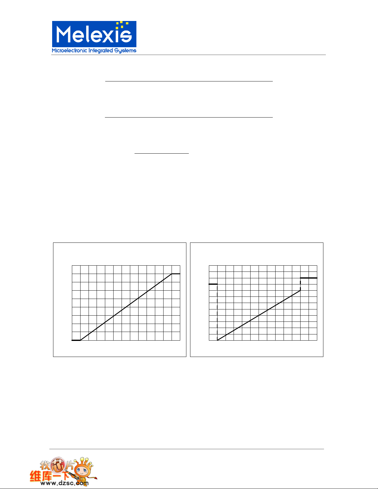
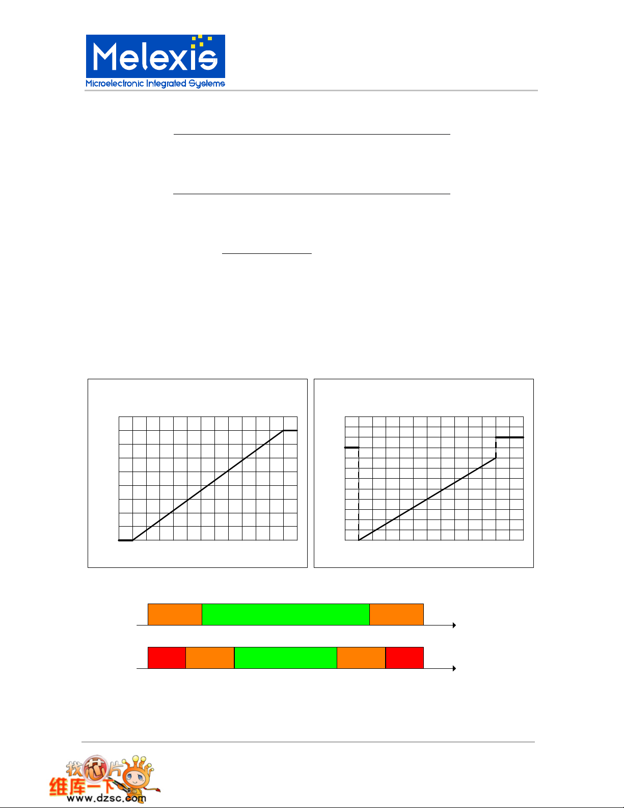
A graphical representation is depicted below.
IROUT output voltage
versus
Object Temperature
4.5
4
3.5
3
2.5
2
1.5
Output Voltage IROUT (V)
1
0.5
0
-40 110 1201008060200-20
40
Object Temperature To (degC)
The behavior of the module outside the calibrated ranges is shown below:
TEMPOUT output voltage
Output Voltage TEMPOUT (V)
versus
Ambient Temperature
4.5
4
3.5
3
2.5
2
1.5
1
0.5
0
Ambient Temperature Ta (degC)
500
T object in
range
T ambient in
range
I I
II I
I or II II
I or II III
-20C
III II
120C
III II IIIIII
50C0C-40C 105C
Tobject
Tambient
Module operating conditions
Effect on outputs
Object temperature output is working normal
Ambient temperature output is working normal
Object temperature output will be clamped 0V (To < -20C) or clamped at 4.5V (T0>120C).
Ambient temperature output is working normal
BOTH temperature outputs will be clamped 0V (Ta < 0C) or clamped at 4.5V (Ta>50C).
The module may be damaged if operated outside the ambient temperature range.
BOTH temperature outputs will be clamped 0V (Ta < 0C) or clamped at 4.5V (Ta>50C).
3901090601 Page 11 of 49 Aug/02
Rev. 007
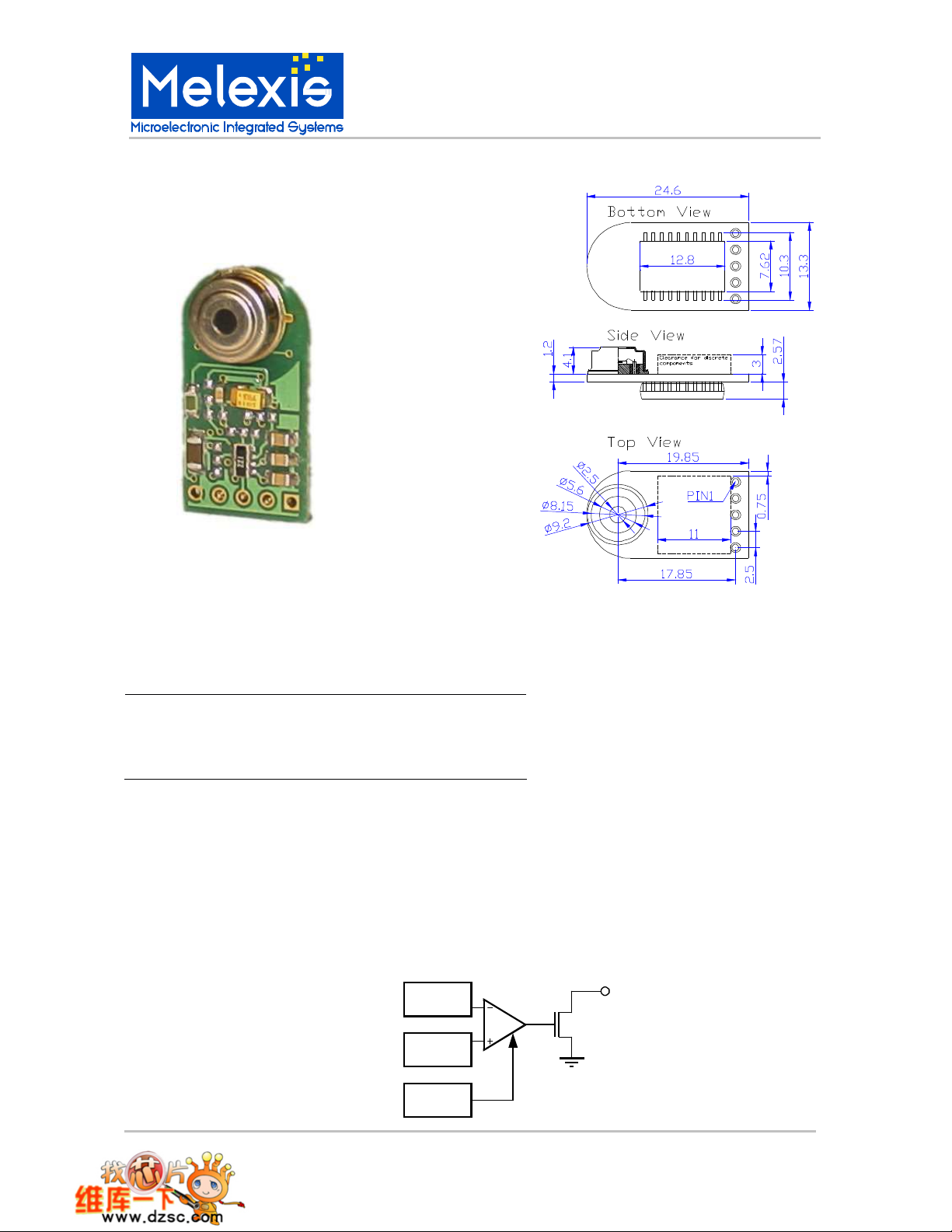
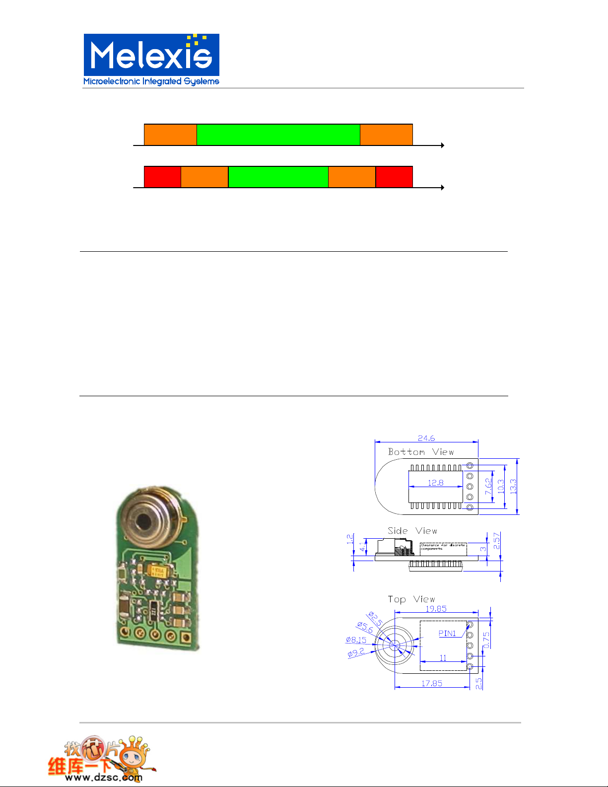
7.3 Physical outline
MLX90601 family
IR thermometer modules
7.4 Pin-out and pin descriptions
pin-out information
pin name function
1 IROUT analog output infrared temperature
2 TEMPOUT analog output ambient temperature
3 VDD Supply voltage
4 REL1 Relay output
5 VSS Ground connection
IROUT IRout analog voltage output pin. The voltage at this pin is a linear representation of Tobject,
the temperature of the object the IR sensor is pointed at.
TEMPOUT Ambient temperature analog voltage output pin. The voltage at this pin is a linear
representation of Tambient, the temperature of the IR sensor, as measured by the PTC
inside MLX90247.
VDD Supply pin
REL1 Open drain relay driver output. The typical on-resistance of this driver is <10 Ohms.
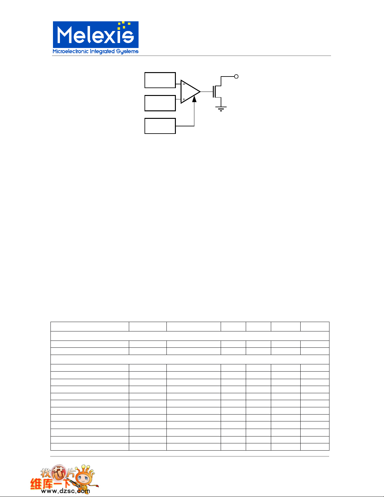
REL1
Tobject
COMP
Threshold in
EEPROM
VSS
Hysteresis
in EEPROM
3901090601 Page 12 of 49 Aug/02
Rev. 007
MLX90601 family
IR thermometer modules
The comparator is a digital comparator, with a resolution of 12 bits. By default the input
polarity is inverting. Threshold and hysteresis values are version dependent. These
settings can be changed by factory programming on request. Refer to calibration settings
for factory preset values.
VSS Supply pin (0V)
7.5 Electrical specifications
Parameter symbol condition min typ max unit
Supply Voltage
Supply voltage range VDD 4.75 5 6 V
Power consumption IDD Ta=25C 5 5.6 mA
analog outputs IROUT/TEMPOUT
D/A converter resolution 8 Bits
Output source current Iod 1 mA
Output sink current Ios 20 uA
AC Output impedance ro 100
Capacitive load Cmax 100 nF
Rel1 open drain relay driver
output impedance Ro 10 Ohms
High voltage protections 32 V
Ω
7.6 Calibration details
Maximum calibrated object temperature 120°C
Minimum calibrated object temperature -20°C
Object temperature Accuracy ±2°C
Maximum calibrated ambient temperature 50°C
Minimum calibrated ambient temperature 0°C
Ambient temperature Accuracy ±1°C
Response time 500ms
REL1 source Tobject
REL1 polarity (*) Inverting
REL1 threshold 50°C
REL1 hysteresis 5°C
Emissivity 0.99
Note: Comparator polarity:
Inverting: relay switches OFF if temperature is above the threshold.
Non-inverting: relay switches ON if temperature is above the threshold.
3901090601 Page 13 of 49 Aug/02
Rev. 007
MLX90601 family
IR thermometer modules
7.7 Applications information
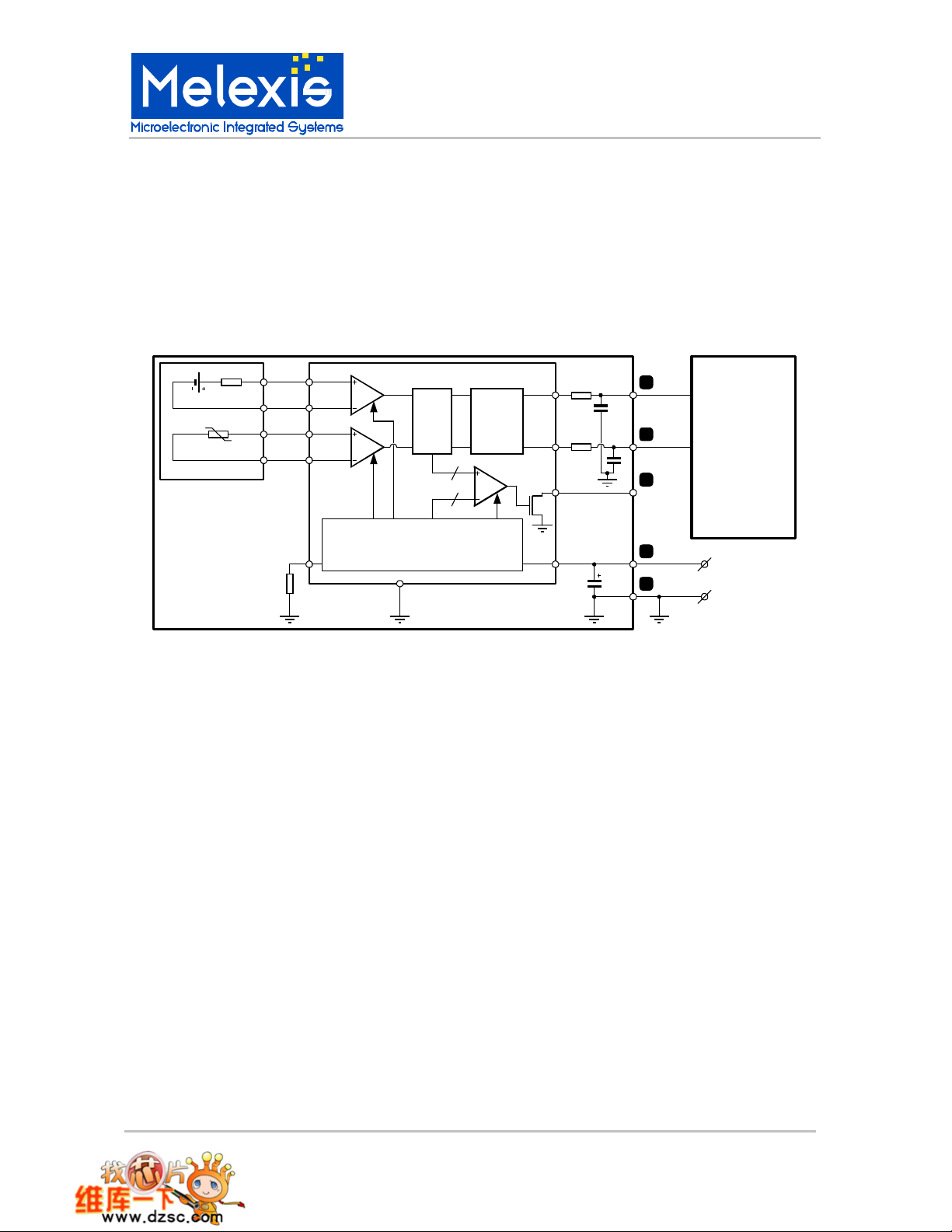
Connection of the MLX90601 module into an application is straightforward. The 5V regulated supply
should be connected between pin 3 (VDD) and pin 5 (VSS).
The outputs can be measured relative to VSS at pin 1 (IROUT) for Tobject and pin 2 (TEMPOUT) for
Tambient, e.g. by means of a voltmeter. In an actual application the module outputs can be directly
connected to the A/D inputs of a microcontroller, e.g. as a replacement for a conventional temperature
sensor.
In many applications, the ambient temperature of the sensor is not needed. In this case, pin 2 can simply
be left open.
The REL1 signal at pin 4 can be used as input for a digital I/O or to drive a relay (not shown). In case of a
digital input the microcontroller must have internal pull-up resistors or an external pull-up resistor must be
added.
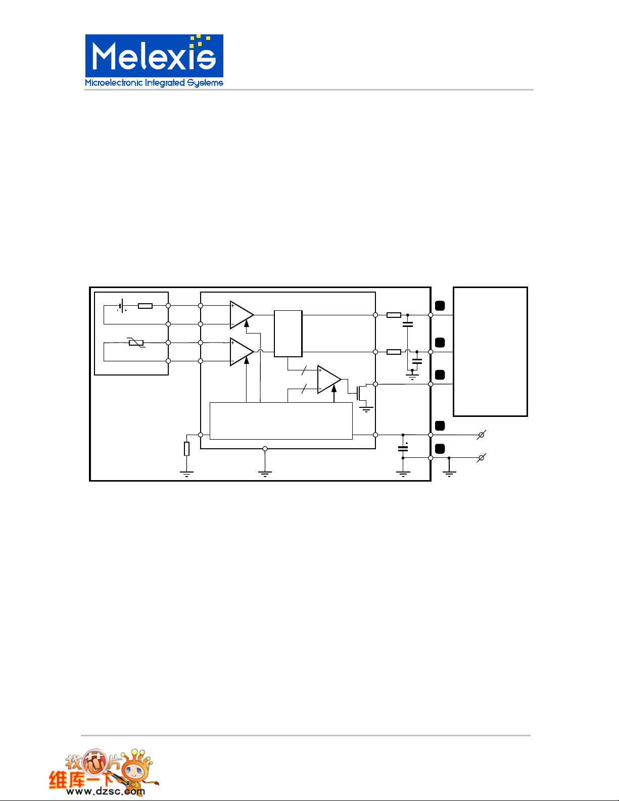
IR sensor
Thermisto
MLX90247
IR+
IR-
r
Rsens
VSS
IRINP
IRINN
TINP
TINN
OPA
OPA
A/D
Digital
A/D
D/A
D/A
Ta
MLX90313
Ta
To
COMP12
TEMPOUT
IROUT
REL1
2
1
4
Application
Microcontroller
A/D input (optional)
A/D input
Digital input
MLX90601B
EEprom, Control and Support Blocks
VSS
VDDCREF
3
5V
5
VSS
3901090601 Page 14 of 49 Aug/02
Rev. 007

MLX90601 family
8
8
8
16
16
IR thermometer modules
8 MLX90601EZA-DAA
8.1 Key properties
• Automotive use
• PWM coded output signals with 10 bit resolution
• ambient temperature underflow and overflow flagging
• relay comparator
• only 5 connections
8.2 General description
The MLX90601EZA-DAA is a module that is targeted for automotive use. In addition to the small amount
of components like the sensor, ASIC etc there are also 2 RC protection circuits on the IROUT and
TEMPOUT pins. This allows the module to be used in automotive environments.
The Object temperature information is available at the IROUT pin. The ambient temperature information is
available on the TEMPOUT pin. The resolution of the Pulse Width Modulated output is 10 bits. Next to
the temperature information, these outputs can also flag ambient temperature underflow and overflow.
The module has an on-board ECC (EEPROM consistency check), that checks the stored calibration
constants and settings. In case of failure, the output fill flag this condition.
If the ambient temperature is out of the calibrated temperature range, both PWM signals will flag this
condition, and the object and ambient temperatures will not be available until the ambient temperature is
back in the calibrated temperature range.
Next to the temperature outputs there is also a relay driver output. The relay driver has a threshold that is
pre-set to 50 °C, with a hysteresis of 5 °C. Note that this module has no SPI interface connector available.
If the user wants to reconfigure this type of module, this can be done with the EVB board and a special
test clip. Refer to appendix A for details.
The PWM coding format is depicted below
t4:Error Signaling Band
Valid Data Output Band
FE
OVH
output signal
t
1
1
T
The PWM signal has a period of 102.4ms typical consisting of 2048 clock cycles of 50µs. Every frame
starts with a leading buffer time, t1, during which the signal is always high, as shown in the figure. The
leading buffer time is followed by a slot for the useful data signal starting at 1/8T ending at 5/8T, where the
ratio t2/(t2+t3) is the representation of the output value. t4 is a slot for signaling of special conditions,
such as out of range measurement of the sensor temperature, Tambient and the occurrence of a fatal
EEPROM error, i.e. an error that can no longer be corrected automatically by the ECC circuitry of
MLX90313.
3901090601 Page 15 of 49 Aug/02
Rev. 007
t
2
t
3
5
OVL
t
5
time
T
T
T
16
12
11
13
7
T
T
T0
MLX90601 family
−
%
50
IR thermometer modules
PWM duty cycle overview
Condition Duty cycle nominal timing
Normal operation 12.5% - 62.5% 12.8 ms - 64 ms
OVL: Tambient underflow 68.75 % 70.4 ms
OVH: Tambient overflow 75 % 76.8 ms
FE: Fatal Error EEPROM 81.25% 83.2 ms
The relation of the output voltage to the temperature is defined as follows:
DutyCycle
T +−
= *
where:
T measured temperature
DutyCycle Duty Cycle of the IROUT or TEMPOUT PWM signals.
Tmin minimal calibrated temperature
Tmax maximum calibrated temperature
Refer to calibration details for calibrated ranges info
A graphical representation is depicted below.
IROUT PWM
versus
Object Temperature
%5.12
( )
TEMPOUT PWM
Ambient Temperature
TminTminTmax
versus
62.5
50
37.5
Duty Cycle IROUT (%)
25
12.5
-20 120
Object Temperature To (degC)
75
62.5
50
37.5
Duty Cycle TEMPOUT (%)
25
12.5
0 50
Ambient Temperature Ta (degC)
3901090601 Page 16 of 49 Aug/02
Rev. 007
MLX90601 family
IR thermometer modules
The behavior of the module outside the calibrated ranges is shown below:
T object in
range
I I
II I
I or II II
I or II III
T ambient in
range
III II
-20C
120C
III II IIIIII
50C0C-40C 105C
Module operating conditions
Effect on outputs
Object temperature output is working normal
Ambient temperature output is working normal
Object temperature output duty cycle will be 12.5% if To < -20C, or 62.5% if To > 120C.
Ambient temperature output is working normal
BOTH temperature outputs duty cycle will be 68.75% if Ta < 0C, or 75% if Ta > 50C.
The module may be damaged if operated outside the ambient temperature range.
BOTH temperature outputs duty cycle will be 68.75% if Ta < 0C, or 75% if Ta > 50C.
Tobject
Tambient
8.3 Physical outline
3901090601 Page 17 of 49 Aug/02
Rev. 007
MLX90601 family
IR thermometer modules
8.4 Pin-out and pin descriptions
pin-out information
pin Name function
1 PWM output infrared temperature
2 PWM output ambient temperature
3 Supply voltage
4 Relay output
5 Ground connection
IROUT IRout PWM coded output pin. The duty cycle of the signal on this pin is a linear
representation of Tobject, the temperature of the object the IR sensor is pointed at.
TEMPOUT Tempout PWM coded output pin. The duty cycle of the signal on this pin is a linear
representation of Tambient, the temperature of the IR sensor, as measured by the PTC
inside MLX90247.
VDD Supply pin
REL1 Open drain relay driver output. The typical on-resistance of this driver is <10 Ohms.
REL1
Tobject
COMP
Threshold in
EEPROM
VSS
Hysteresis
in EEPROM
The comparator is a digital comparator, with a resolution of 12 bits. By default the input
polarity is inverting. Threshold and hysteresis values are version dependent. These
settings can be changed by factory programming on request. Refer to calibration settings
for factory preset values.
VSS Supply pin (0V)
8.5 Electrical specifications
Parameter symbol condition min typ max unit
Supply Voltage
Supply voltage range VDD 4.75 5 6 V
Power consumption IDD Ta=25C 5 5.6 mA
outputs IROUT/TEMPOUT
PWM modulator resolution 10 bits
PWM Clock period Tclk 45 50 55
PWM Total period T 92.16 102.4 112.64 ms
Leading buffer time t1 % of T 12.5
Trailing buffer time t5 % of T 12.5
Duty cycle high t2 % of T 0 50 %
µs
%
%
3901090601 Page 18 of 49 Aug/02
Rev. 007

MLX90601 family
IR thermometer modules
Parameter symbol condition min typ max unit
Duty cycle low t3 % of T 0 50 %
Error signal t4 % of T 25
Rise time* 10% to 90% of Vh 13.3 100
Fall time* 90% to 10% of Vh 13.3 100
Output voltage high Vh Ihigh=2mA 4 V
Output voltage low Vl Ilow=2mA 1 V
Rel1 open drain relay driver
output impedance Ro 10 Ohms
High voltage protections 32 V
* no external load
8.6 Calibration details
Maximum calibrated object temperature 120°C
Minimum calibrated object temperature -20°C
Object temperature Accuracy ±2°C
Maximum calibrated ambient temperature 50°C
Minimum calibrated ambient temperature 0°C
Ambient temperature Accuracy ±1°C
Response time 500ms
REL1 source Tobject
REL1 polarity (*) Inverting
REL1 threshold 50°C
REL1 hysteresis 5°C
Emissivity 0.99
Note: Comparator polarity:
Inverting: relay switches OFF if temperature is above the threshold.
Non-inverting: relay switches ON if temperature is above the threshold.
%
µs
µs
3901090601 Page 19 of 49 Aug/02
Rev. 007
MLX90601 family
IR thermometer modules
8.7 Applications information
Connection of the MLX90601 module into an application is. The 5V regulated supply should be connected
between pin 3 (VDD) and pin 5 (VSS).
In an actual application the module outputs can be directly connected to a timer or IRQ inputs of a
microcontroller. In many applications, the ambient temperature of the sensor is not needed. In this case,
pin 2 can simply be left open.
The REL1 signal at pin 4 can be used as input for a digital I/O or to drive a relay (not shown). In case of a
digital input the microcontroller must have internal pull-up resistors or an external pull-up resistor must be
added.
IR sensor
Thermisto
MLX90247
IR+
IR-
r
Rsens
VSS
IRINP
IRINN
TINP
TINN
OPA
OPA
A/D
Digital
A/D
D/A
D/A
Ta
MLX90313
Ta
PWM
To
COMP12
TEMPOUT
IROUT
REL1
2
1
4
Application
Microcontroller
Timer input (optional)
Timer input
MLX90601
EEprom, Control and Support Blocks
VSS
VDDCREF
3
5V
5
VSS
3901090601 Page 20 of 49 Aug/02
Rev. 007
MLX90601 family
8
8
8
16
16
IR thermometer modules
9 MLX90601EZA-CAA
9.1 Key properties
• consumer and industrial use
• PWM output signals with 10 bit resolution
• SPI interface available
• relay comparator and reference voltage
• 10 pole, mating to 1mm pitch flat cable connector
9.2 General description
The MLX90601EZA-CAA is a module that is targeted for industrial and consumer products use. The
sensor and the MLX90313 ASIC are placed on a rigid PCB. The module has a 10 pole connector, which
has all relevant interconnections to the ASIC. There are 2 temperature signals which are preset to provide
digital PWM code output signals. The resolution of the Pulse Width Modulated output is 10 bits. Next to
the temperature information these outputs can also flag ambient temperature underflow and overflow. The
module has an on-board ECC (EEPROM consistency check), that checks the stored calibration constants
and settings. In case of failure, the output fill flag this condition.
If the ambient temperature is out of the calibrated temperature range, both PWM signals will flag this
condition, and the object and ambient temperatures will not be available until the ambient temperature is
back in the calibrated temperature range.
The CAA type module has the SPI interface available. Next to reading the temperature information, the
SPI interface also allows changing the module’s settings and calibration.
Next to the temperature outputs and SPI interface there is also a relay driver output. The relay driver has
a threshold that is pre-set to 50°C, with a hysteresis of 5°C.
The PWM coding format is depicted below
t4:Error Signaling Band
Valid Data Output Band
FE
OVH
output signal
t
1
1
T
The PWM signal has a period of 102.4ms typical consisting of 2048 clock cycles of 50µs. Every frame
starts with a leading buffer time, t1, during which the signal is always high, as shown in the figure. The
leading buffer time is followed by a slot for the useful data signal starting at 1/8T ending at 5/8T, where the
ratio t2/(t2+t3) is the representation of the output value. t4 is a slot for signaling of special conditions,
such as out of range measurement of the sensor temperature, Tambient and the occurrence of a fatal
EEPROM error, i.e. an error that can no longer be corrected automatically by the ECC circuitry of
MLX90313.
3901090601 Page 21 of 49 Aug/02
Rev. 007
t
2
t
3
5
OVL
t
5
time
T
T
T
16
12
11
13
7
T
T
T0
MLX90601 family
−
%
50
IR thermometer modules
PWM duty cycle overview
Condition Duty cycle nominal timing
Normal operation 12.5% - 62.5% 12.8 ms - 64 ms
OVL: Tambient underflow 68.75 % 70.4 ms
OVH: Tambient overflow 75 % 76.8 ms
FE: Fatal Error EEPROM 81.25% 83.2 ms
The relation of the output voltage to the temperature is defined as follows:
DutyCycle
T +−
= *
where:
T measured temperature
DutyCycle Duty Cycle of the IROUT or TEMPOUT PWM signals.
Tmin minimal calibrated temperature
Tmax maximum calibrated temperature
Refer to calibration details for calibrated ranges info
A graphical representation is depicted below.
IROUT PWM
versus
Object Temperature
%5.12
( )
TEMPOUT PWM
Ambient Temperature
TminTminTmax
versus
62.5
50
37.5
Duty Cycle IROUT (%)
25
12.5
-20 120
Object Temperature To (degC)
75
62.5
50
37.5
Duty Cycle TEMPOUT (%)
25
12.5
0 50
Ambient Temperature Ta (degC)
3901090601 Page 22 of 49 Aug/02
Rev. 007

MLX90601 family
CS
IR thermometer modules
The behavior of the module outside the calibrated ranges is shown below:
T object in
range
T ambient in
range
I I
II I
I II
I III
-20C
III II
120C
III II IIIIII
50C0C-40C 105C
Tobject
Tambient
Module operating conditions
Effect on outputs
Object temperature output is working normal
Ambient temperature output is working normal
Object temperature output duty cycle will be 12.5% if To < -20C, or 62.5% if To > 120C.
Ambient temperature output is working normal
SPI IROUT register data bits 0x000 if To < -20C, or 0xFFF if To > 120C.
SPI TOUT register operating normal
BOTH temperature outputs duty cycle will be 68.75% if Ta < 0C, or 75% if Ta > 50C.
SPI IROUT register data bits 0x000 if Ta < 0C, or 0xFFF if Ta > 50C. Corresponding
overflow flags will be set.
The module may be damaged if operated outside the ambient temperature range.
BOTH temperature outputs duty cycle will be 68.75% if Ta < 0C, or 75% if To > 50C.
SPI IROUT register data bits 0x000 if Ta < 0C, or 0xFFF if Ta > 50C. Corresponding
overflow flags will be set.
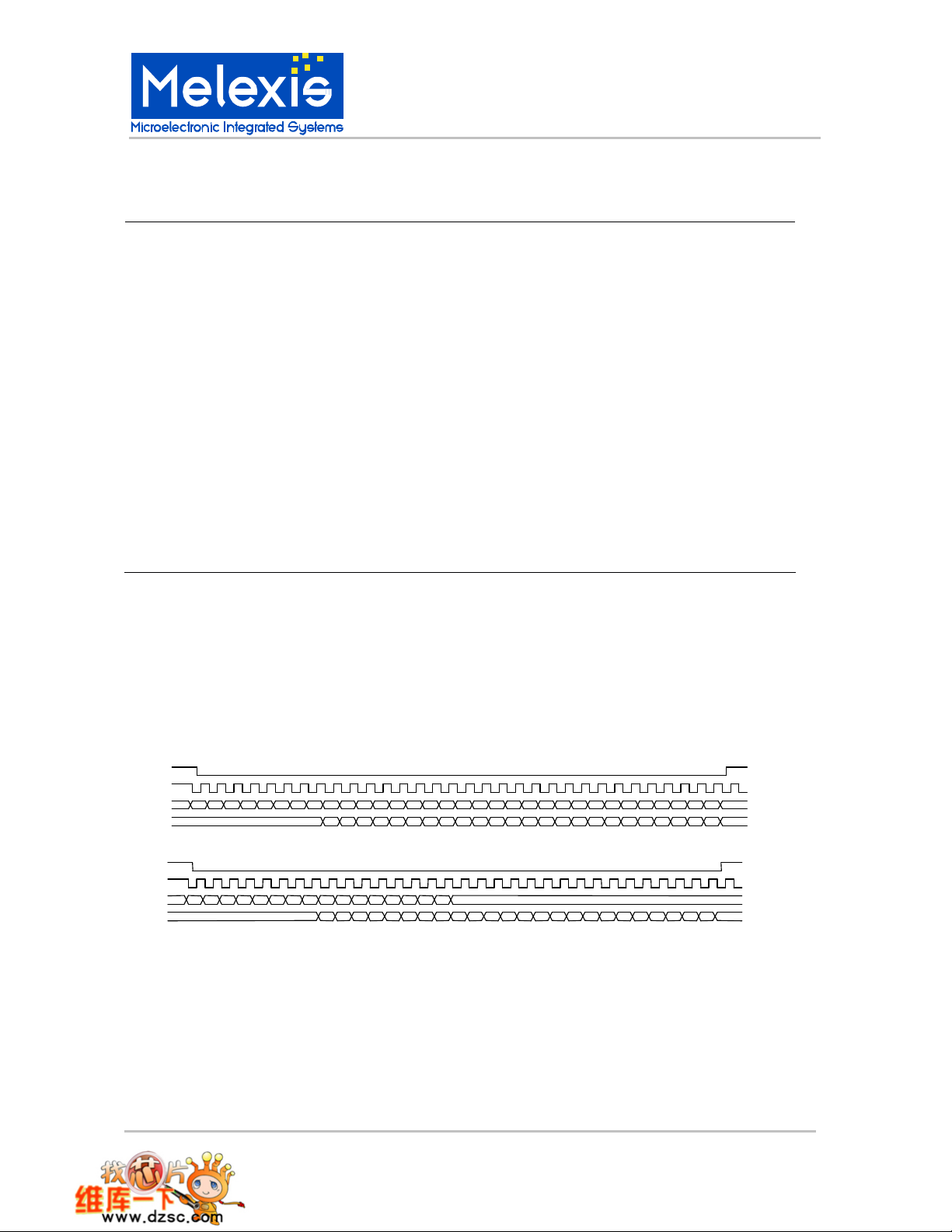
9.3 Serial Peripheral Interface (SPI)
Protocol
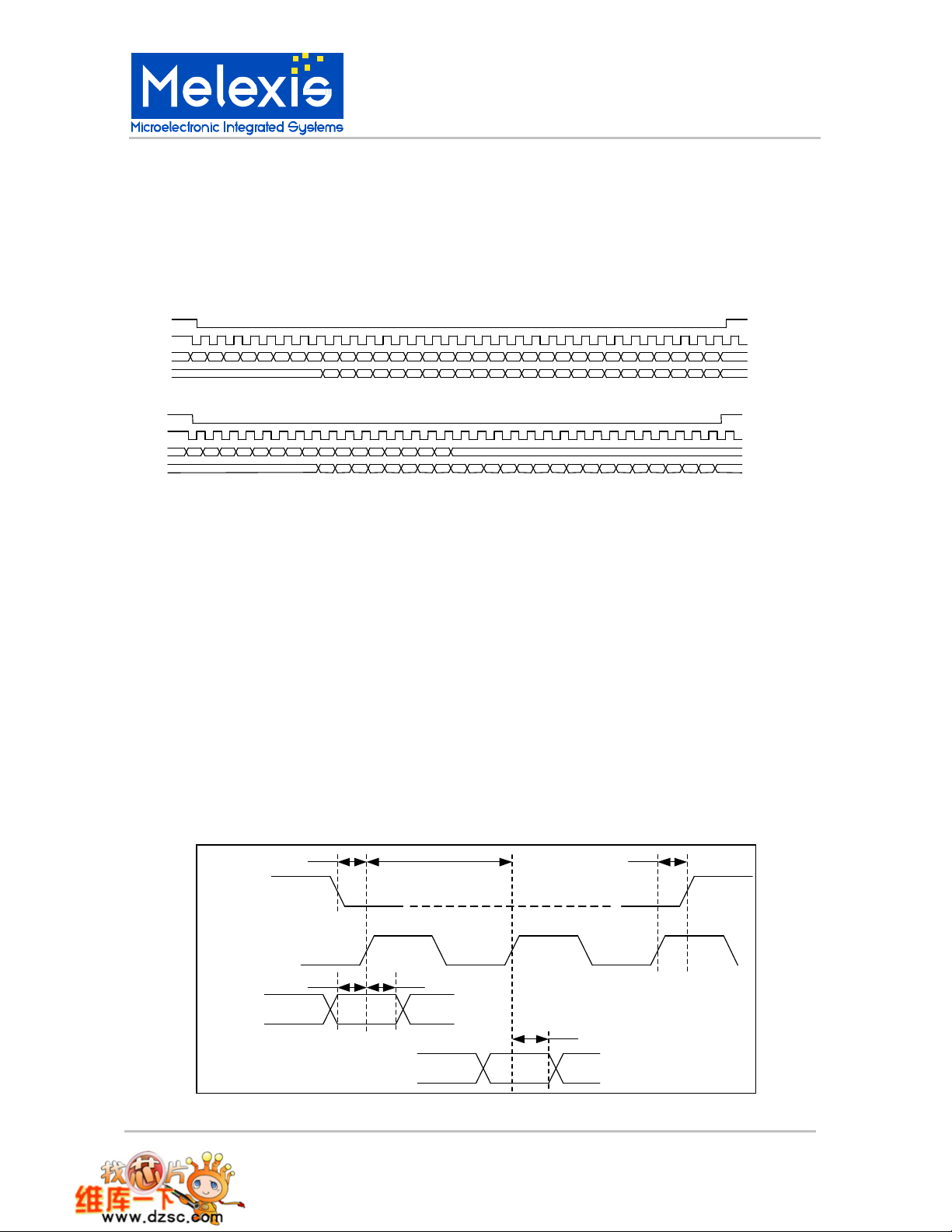
The digital interface implemented in MLX90313C is SPI compatible. It can be used to access the on-chip
EEPROM and all internal registers. The chip will always work as a slave device. The format of any
command is always 32 bits: 8 bits for the operation code, 8 bits for the address and 16 bits of data. The
communication protocol is presented below.
CS
SCLK
SDI
C7 C0C1C2C3C4C5C6 A7 A0A1A2A3A4A5A6 D15 D8D9D10D11D12D13D14 D7 D0D1D2D3D4D5D6 X
SDO C7 C0C1C2C3C4C5C6 A7 A0A1A2A3A4A5A6 D15 D8D9D10D11D12D13D14X X
write command
SCLK
C7 C0C1C2C3C4C5C6 A7 A0A1A2A3A4A5A6 X
SDI
SDO
C7 C0C1C2C3C4C5C6 D7 D0D1D2D3D4D5D6D15 D8D9D10D11D12D13D14X X
read command
3901090601 Page 23 of 49 Aug/02
Rev. 007
MLX90601 family
IR thermometer modules
Every write command starts with a high to low transition of CS and ends by a low to high transition of CS
after 32 periods of the serial data clock (SCLK). MLX90313C reads the data present on SDI on the rising
edge of the clock. With a delay of 8 periods of the serial clock, the SPI will repeat the opcode, address
and the first 8 bits of data on pin SDO. This allows the external master to check command and address
and terminate the operation in case of an error by forcing CS high before the end of the complete
command cycle, i.e. before the end of the 32 clock periods.
The read command is build up similarly, except that no data has to be passed of course. On SDO the
opcode will be followed directly by the requested data, the address is not returned in this case.
The data on SDO is valid on the rising edge of the clock. In case of a read command, the SPI will output
the data on SDO starting on the 25th rising edge of the clock (after CS low) as indicated in the figure
above.
Timing/speed
The baud-rate depends on the serial data clock (SCLK) supplied by the master controller and is limited to
125kb/s. The timing requirements are given in the figure and table below
tsclktcls tsch
CS
SCLK
tsu thd
SDI
tdv
SDO
SPI timing
SPI timing requirements
Symbol Parameter Value Unit
tsclk Sclk period min 8
tcls CS low to SCLK high min 50 ns
tsch SCLK low to CS high min 50 ns
tsu data in setup time min 200 ns
thd data in hold time min 200 ns
tdv data out valid min 1
operation codes
The operation code is the first series of 8bits in a command, C[7:0] in the figure on the protocol above.
Below table summarizes the operations available in MLX90313C.
Operation Codes
mnem. C[7:0] Command
WR
X101X0XX
Write internal register
µs
µs
3901090601 Page 24 of 49 Aug/02
Rev. 007
MLX90601 family
−=1
2
IR thermometer modules
RD
WEPR
ER
REPR
BLWR
BLER
Temperature registers
The object and ambient temperatures are stored into internal registers.
A table containing the most interesting internal register addresses is included below:
Address list internal registers
Register Function Address
Irout Tobject (lin) 09h
Tout Tambient (lin) 0Ah
These registers keep the linearised object and ambient temperature.
Register format:
Bit 15 14 13 12 11 10 9 8 7 6 5 4 3 2 1 0
Name D11 D10 D9 D8 D7 D6 D5 D4 D3 D2 D1 D0 OVH OVL FE Res
D11..D0 : 12 bit temperature data
OVH: Overflow flag for Tambient measurement, Ta>Tamax, D[11:0] set to FFFh
OVL: Underflow flag for Tambient measurement, Ta<Tamin, D[11:0] set to 000h
FE: Fatal Error in EEPROM.
Res Not used, always zero.
The measured temperature can be obtained from the register content as follows:
Where:
Rt register value (12 bit, 0x000 to 0xFFF)
Tmax maximum calibrated temperature
Tmin minimum calibrated temperature
EEPROM reprogramming
Every MLX90601 module has 8 words of 16bits of EEPROM space free to use for the user. One can
freely use this memory space for serialization or storing some other info. Also, in some cases it is
necessary to redefine functionality of the MLX90601 infrared module.
The configuration constants are stored in EEPROM non-volatile memory. Note that also the linearization
constants are stored in EEPROM, and erasing or over-writing these will irreversible destroy the modules’
proper operation. Reprogramming the EEPROM must be done with care.
Here’s how to rewrite a specific EEPROM address.
1. Write 0xB200 to register address 0x10. This unlocks EEPROM control registers. The module now
stops updating it’s output
2. Write 0x0065 to register address 0x18. Enables charge pump for programming.
X10010XX
0001XXXX
001XXXXX
X0001XXX
1001XXXX
101XXXXX
Rt
T +−
12
Read internal register
Write EEPROM
Erase EEPROM
Read EEPROM
Block Write EEPROM
Block erase EEPROM
TminTmin)(Tmax
3901090601 Page 25 of 49 Aug/02
Rev. 007

MLX90601 family
IR thermometer modules
3. Erase the address you want to rewrite
4. Write the new data in the EEPROM address
5. Repeat steps 3 and 4 for any further programming
6. You now can cycle the power for restarting the chip in normal operation, with new settings
Be sure never to use the Block Write or Block Erase commands, as they completely erase the EEPROM.
For further details please refer to MLX90313 datasheet.
9.4 Physical outline
9.5 Pin-out and pin descriptions
pin-out information
pin name Function
1 REL1 Relay output
2 VSS Ground connection
3 VDD Supply voltage
4 SDIN SPI data in
5 SDOUT SPI data out
6 CSB SPI chip select
7 SCLK SPI clock
8 IROUT PWM coded output infrared
temperature
9 VREF Reference voltage output
10 TEMPOUT PWM coded output ambient
temperature
REL1 Open drain relay driver output. The typical on-resistance of this driver is <10
Ohms.
3901090601 Page 26 of 49 Aug/02
Rev. 007
MLX90601 family
dependent. These settings can be changed by factory programming on request.
IR thermometer modules
REL1
Tobject
COMP
Threshold in
EEPROM
VSS
Hysteresis
in EEPROM
The comparator is a digital comparator, with a resolution of 12 bits. By default
the input polarity is inverting. Threshold and hysteresis values are version
Refer to calibration settings for factory preset values.
VSS Supply pin (0V)
VDD Supply pin
SDIN SPI data input
SDOUT SPI data output
CSB SPI chip select. Active low.
SCLK SPI clock line
IROUT IRout PWM coded output pin. The duty cycle of the signal on this pin is a linear
representation of Tobject, the temperature of the object the IR sensor is pointed
at.
VREF DAC reference voltage. This voltage must be used if the module is used as a
thermostat using the REL1 comparator with external threshold.
TEMPOUT Tempout PWM coded output pin. The duty cycle of the signal on this pin is a
linear representation of Tambient, the temperature of the IR sensor, as
measured by the PTC inside MLX90247.
9.6 Electrical specifications
Parameter symbol condition min typ max unit
Supply Voltage
Supply voltage range VDD 4.75 5 6 V
Power consumption IDD Ta=25C 5 5.6 mA
outputs IROUT/TEMPOUT
PWM modulator resolution 10 bits
PWM Clock period Tclk 45 50 55
PWM Total period T 92.16 102.4 112.64 ms
Leading buffer time t1 % of T 12.5
Trailing buffer time t5 % of T 12.5
Duty cycle high t2 % of T 0 50 %
Duty cycle low t3 % of T 0 50 %
Error signal t4 % of T 25
Rise time* 10% to 90% of Vh 13.3 100
Fall time* 90% to 10% of Vh 13.3 100
Output voltage high Vh Ihigh=2mA 4 V
Output voltage low Vl Ilow=2mA 1 V
3901090601 Page 27 of 49 Aug/02
Rev. 007
µs
%
%
%
µs
µs

MLX90601 family
IR thermometer modules
Parameter symbol condition min typ max unit
Rel1 open drain relay driver
output impedance Ro 10 Ohms
High voltage protections 32 V
9.7 Calibration details
Maximum calibrated object temperature 120°C
Minimum calibrated object temperature -20°C
Object temperature Accuracy ±2°C
Maximum calibrated ambient temperature 0°C
Minimum calibrated ambient temperature 50°C
Ambient temperature Accuracy ±1°C
Response time 500ms
REL1 source Tobject
REL1 polarity (*) Inverting
REL1 threshold 50°C
REL1 hysteresis 5°C
Emissivity 0.99
Note: Comparator polarity:
Inverting: relay switches OFF if temperature is above the threshold.
Non-inverting: relay switches ON if temperature is above the threshold.
3901090601 Page 28 of 49 Aug/02
Rev. 007

MLX90601 family
IR thermometer modules
9.8 Applications information
Connection of the MLX90601EZA-CAA module into an application is straightforward. The 5V regulated
supply should be connected between pin 3 (VDD) and pin 2 (VSS). There are numerous possibilities for
the I/O of which one example is shown below. Here the default configuration is used. In the example a
relay is switched with the REL1 output. The threshold for this comparator is programmed in the EEPROM.
This means the microcontroller can change the threshold, and the MLX90601 can control the alarm
standalone. The SPI connection to the host microcontroller can be a permanent connection in the
application or just a means for in-circuit programming of the device. Through this connection full access
to the internal registers and configuration settings is achieved. The SPI connection can also be used to
directly read output data from the module in digital form and process this directly in the application. An
interesting feature is in-circuit programming of the calibration constants. It is possible to change the range
or emissivity, or whatever setting needs to be user adjustable.
IR sensor
Thermisto
MLX90247
IR+
IR-
r
Rsens
VSS
IRINP
IRINN
TINP
TINN
OPA
OPA
A/D
Digital
A/D
PWM
PWM
MLX90313C
To
COMP
REL1
TEMPOUT
IROUT
1
10
8
SW1
SW2
VCM25V
VSS
Control and Support Blocks
SPI
VREFP
VDDCREF
4 5 6 7SPI
Micro-controller I/O-port
9
3
2
PWM IN
PWM IN
Vref
5V
VSS
3901090601 Page 29 of 49 Aug/02
Rev. 007

MLX90601 family
5.4
IR thermometer modules
10 MLX90601KZA-BKA
10.1 Key properties
• Flex circuit for consumer and industrial use.
• analog output signals with 8 bit resolution
• SPI interface available
• relay comparator and reference voltage
• 10 pole flex connector
10.2 General description
The MLX90601KZA-BKA is a module that is targeted for industrial and consumer products use. The
sensor and the MLX90313 ASIC are placed on a flexible substrate. This allows the sensor to be bent in
any direction. This may greatly simplify fitting in the module into the application.
The module has a 10 pole connector, which has all relevant interconnections to the ASIC. There are 2
temperature signals which are preset to provide analog output voltage. The Object temperature
information is available at the IROUT pin. The ambient temperature information is available on the
TEMPOUT pin. The resolution of the output D/A converter is 8bit. The output drivers have a maximum
output voltage of 4.5V when the maximum calibrated temperature is reached.
If the ambient temperature is out of the calibrated temperature range, the correct object temperature
cannot be calculated. For applications where the ambient temperature can rise above the maximum
calibrated temperature, the ambient temperature output must be monitored to make sure the object
temperature is valid.
The flex modules all have the SPI interface available. Next to reading the temperature information, the
SPI interface also allows changing the module’s settings and calibration.
The temperature as read by the SPI interface will not be equal to the temperature presented at the analog
outputs. Refer to SPI interface description for details.
Next to the temperature outputs there is also a relay driver output. The relay driver has a threshold that is
pre-set to 95°C, with a hysteresis of 5°C.
The relation of the output voltage to the temperature is defined as follows:
Vout
T +−= *
( )
TminTminTmax
Where:
T measured temperature
Vout analog output voltage on IROUT or TEMPOUT pins.
Tmin minimal calibrated temperature
Tmax maximum calibrated temperature
Refer to calibration details for calibrated ranges info
3901090601 Page 30 of 49 Aug/02
Rev. 007

MLX90601 family
IR thermometer modules
A graphical representation is depicted below.
IROUT output voltage
versus
Object Temperature
4.5
4
3.5
3
2.5
2
1.5
Output Voltage IROUT (V)
1
0.5
0
-40
40
Object Temperature To (degC)
110 1201008060200-20
The behavior of the module outside the calibrated ranges is shown below:
TEMPOUT output voltage
versus
Ambient Temperature
4.5
4
3.5
3
2.5
2
1.5
1
Output Voltage TEMPOUT (V)
0.5
0
Ambient Temperature Ta (degC)
85-20
-20C
III II
120C
III II IIIIII
85C-20C-40C 125C
Tobject
Tambient
Module operating conditions
T object in
range
I I
T ambient in
range
Effect on outputs
Object temperature output is working normal
Ambient temperature output is working normal
II I
Object temperature output will be clamped at 0V (To < -20C) or clamped at 4.5V
(T0>120C).
Ambient temperature output is working normal
SPI IROUT register data bits 0x000 if To < -20C, or 0xFFF if To > 120C.
SPI TOUT register operating normal
I or II II
BOTH temperature outputs will be clamped 0V (Ta < -20C) or clamped at 4.5V (Ta>85C).
SPI IROUT register data bits 0x000 if Ta < -20C, or 0xFFF if Ta > 85C. Corresponding
overflow flags will be set.
I or II III
The module may be damaged if operated outside the ambient temperature range.
BOTH temperature outputs will be clamped 0V (Ta < -20C) or clamped at 4.5V (Ta>85C).
SPI IROUT register data bits 0x000 if Ta < -20C, or 0xFFF if Ta > 85C. Corresponding
overflow flags will be set.
3901090601 Page 31 of 49 Aug/02
Rev. 007
MLX90601 family
CS
IR thermometer modules
10.3 Serial Peripheral Interface (SPI)
Protocol
The digital interface implemented in MLX90313C is SPI compatible. It can be used to access the on-chip
EEPROM and all internal registers. The chip will always work as a slave device. The format of any
command is always 32 bits: 8 bits for the operation code, 8 bits for the address and 16 bits of data. The
communication protocol is presented below.
CS
SCLK
SDI
C7 C0C1C2C3C4C5C6 A7 A0A1A2A3A4A5A6 D15 D8D9D10D11D12D13D14 D7 D0D1D2D3D4D5D6 X
SDO C7 C0C1C2C3C4C5C6 A7 A0A1A2A3A4A5A6 D15 D8D9D10D11D12D13D14X X
Write command
SCLK
C7 C0C1C2C3C4C5C6 A7 A0A1A2A3A4A5A6 X
SDI
SDO
C7 C0C1C2C3C4C5C6 D7 D0D1D2D3D4D5D6D15 D8D9D10D11D12D13D14X X
Read command
Every write command starts with a high to low transition of CS and ends by a low to high transition of CS
after 32 periods of the serial data clock (SCLK). MLX90313C reads the data present on SDI on the rising
edge of the clock. With a delay of 8 periods of the serial clock, the SPI will repeat the opcode, address
and the first 8 bits of data on pin SDO. This allows the external master to check command and address
and terminate the operation in case of an error by forcing CS high before the end of the complete
command cycle, i.e. before the end of the 32 clock periods.
The read command is build up similarly, except that no data has to be passed of course. On SDO the
opcode will be followed directly by the requested data, the address is not returned in this case.
The data on SDO is valid on the rising edge of the clock. In case of a read command, the SPI will output
the data on SDO starting on the 25th rising edge of the clock (after CS low) as indicated in the figure
above.
Timing/speed
The baud-rate depends on the serial data clock (SCLK) supplied by the master controller and is limited to
125kb/s. The timing requirements are given in the figure and table below
=
tsclktcls tsch
CS
SCLK
tsu thd
SDI
tdv
SDO
SPI timing
3901090601 Page 32 of 49 Aug/02
Rev. 007
MLX90601 family
IR thermometer modules
SPI timing requirements
Symbol Parameter Value Unit
tsclk Sclk period min 8
tcls CS low to SCLK high min 50 ns
tsch SCLK low to CS high min 50 ns
tsu data in setup time min 200 ns
thd data in hold time min 200 ns
tdv data out valid min 1
operation codes
The operation code is the first series of 8bits in a command, C[7:0] in the figure on the protocol above.
Below table summarizes the operations available in MLX90313C.
Operation Codes
mnem. C[7:0] Command
WR
RD
WEPR
ER
REPR
BLWR
BLER
Temperature registers
The object and ambient temperatures are stored into internal registers.
A table containing the most interesting internal register addresses is included below:
Address list internal registers
Register Function Address
Irout Tobject (lin) 09h
Tout Tambient (lin) 0Ah
X101X0XX
X10010XX
0001XXXX
001XXXXX
X0001XXX
1001XXXX
101XXXXX
Write internal register
Read internal register
Write EEPROM
Erase EEPROM
Read EEPROM
Block Write EEPROM
Block erase EEPROM
These registers keep the linearised object and ambient temperature.
Register format:
Bit 15 14 13 12 11 10 9 8 7 6 5 4 3 2 1 0
Name D11 D10 D9 D8 D7 D6 D5 D4 D3 D2 D1 D0 OVH OVL FE Res
D11..D0 : 12 bit temperature data
OVH: Overflow flag for Tambient measurement, Ta>Tamax, D[11:0] set to FFFh
OVL: Underflow flag for Tambient measurement, Ta<Tamin, D[11:0] set to 000h
FE: Fatal Error in EEPROM.
Res Not used, always zero.
The MLX90601 KZA-BKA has been calibrated to have absolute voltage outputs. Therefore there is a
difference between the temperature information of the analog outputs and the internal register values.
µs
µs
3901090601 Page 33 of 49 Aug/02
Rev. 007

MLX90601 family
−=1
2
IR thermometer modules
Before calculation of the temperature for the internal register content is possible, it is necessary to
measure the VREF voltage, available at pin 5. This voltage will be slightly different for each module so it
must be measured for every module. A correction factor must be included in the calculation.
The measured temperature can be obtained from the register content as follows:
Vref
*
Rt
T +−•
Where:
T measured temperature
Rt register value (12 bit, 0x000 to 0xFFF)
Vref Reference voltage (to be measured)
Tmax maximum calibrated temperature
Tmin minimum calibrated temperature
EEPROM reprogramming
Every MLX90601 module has 8 words of 16bits of EEPROM space free to use for the user. One can
freely use this memory space for serialization or storing some other info. Also, in some cases it is
necessary to redefine functionality of the MLX90601 infrared module.
The configuration constants are stored in EEPROM non-volatile memory. Note that also the linearization
constants are stored in EEPROM, and erasing or over-writing these will irreversible destroy the modules’
proper operation. Reprogramming the EEPROM must be done with care.
Here’s how to rewrite a specific EEPROM address.
7. Write 0xB200 to register address 0x10. This unlocks EEPROM control registers. The module now
stops updating it’s output
8. Write 0x0065 to register address 0x18. Enables charge pump for programming.
9. Erase the address you want to rewrite
10. Write the new data in the EEPROM address
11. Repeat steps 3 and 4 for any further programming
12. You now can cycle the power for restarting the chip in normal operation, with new settings
Be sure never to use the Block Write or Block Erase commands, as they completely erase the EEPROM.
For further details please refer to MLX90313 datasheet.
5.4
12
TminTmin)(Tmax
3901090601 Page 34 of 49 Aug/02
Rev. 007
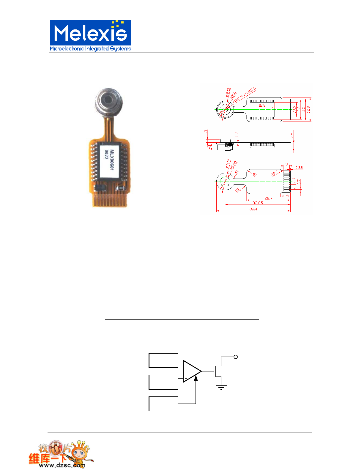
10.4 Physical outline
MLX90601 family
IR thermometer modules
10.5 Pin-out and pin descriptions
pin-out information
pin name function
1 VSS Ground connection
2 REL1 Relay output
3 IROUT analog output infrared temperature
4 TEMPOUT analog output ambient temperature
5 VREF Reference voltage output
6 VDD Supply voltage
7 SDIN SPI data in
8 SCLK SPI clock
9 SDOUT SPI data out
10 CSB SPI chip select
VSS Supply pin (0V)
REL1 Open drain relay driver output. The typical on-resistance of this driver is <10 Ohms.
REL1
Tobject
COMP
Threshold in
EEPROM
VSS
Hysteresis
in EEPROM
The comparator is a digital comparator, with a resolution of 12 bits. By default the input
3901090601 Page 35 of 49 Aug/02
Rev. 007
MLX90601 family
IR thermometer modules
polarity is inverting. Threshold and hysteresis values are version dependent. These
settings can be changed by factory programming on request. Refer to calibration settings
for factory preset values.
IROUT IRout analog voltage output pin. The voltage at this pin is a linear representation of Tobject,
the temperature of the object the IR sensor is pointed at.
TEMPOUT Ambient temperature analog voltage output pin. The voltage at this pin is a linear
representation of Tambient, the temperature of the IR sensor, as measured by the PTC
inside MLX90247.
VREF DAC reference voltage. This voltage must be used if the module is used as a thermostat
using the REL1 comparator with external threshold.
VDD Supply pin
SDIN SPI data input
SCLK SPI clock line
SDOUT SPI data output
CSB SPI chip select. Active low.
10.6 Electrical specifications
Parameter symbol condition min typ max unit
Supply Voltage
Supply voltage range VDD 4.75 5 6 V
Power consumption IDD Ta=25C 5 5.6 mA
analog outputs IROUT/TEMPOUT
D/A converter resolution 8 Bits
Output source current Iod 1 mA
Output sink current Ios 20 uA
AC Output impedance ro 100
Capacitive load Cmax directly on pin 50 pF
Capacitive load with 200 ohms
series resistance
Rel1 open drain relay driver
output impedance Ro 10 Ohms
High voltage protections 32 V
When the Cmax value is exceeded, a series resistor must be used to maintain stability.
100 nF
Ω
10.7 Calibration details
Maximum calibrated object temperature 120°C
Minimum calibrated object temperature -20°C
Object temperature Accuracy ±2°C
Maximum calibrated ambient temperature -20°C
Minimum calibrated ambient temperature 85°C
Ambient temperature Accuracy ±1°C
Response time 500ms
REL1 source Tobject
REL1 polarity (*) Inverting
REL1 threshold 95°C
REL1 hysteresis 5°C
Emissivity 0.99
3901090601 Page 36 of 49 Aug/02
Rev. 007
MLX90601 family
IR thermometer modules
Note: Comparator polarity:
Inverting: relay switches OFF if temperature is above the threshold.
Non-inverting: relay switches ON if temperature is above the threshold.
10.8 Applications information
Connection of the MLX90601 module into an application is straightforward. The 5V regulated supply
should be connected between pin 6 (VDD) and pin 1 (VSS).
The outputs can be measured relative to VSS at pin 3 (IROUT) for Tobject and pin 4 (TEMPOUT) for
Tambient, e.g. by means of a voltmeter. In an actual application the module outputs can be directly
connected to the A/D inputs of a microcontroller, e.g. as a replacement for a conventional temperature
sensor. When large loading capacitances are to be used, a series resistor may be necessary. Refer to
electrical specifications.
Although the circuit carrier is flexible, it is only intended to be bent at the neck between the thermopile
sensor and the ASIC. Minimal bending radius is 1.5mm.
In many applications, the ambient temperature of the sensor is not needed. In this case, pin 2 can simply
be left open.
The REL1 signal can be used as input for a digital I/O or to drive a relay (not shown). In case of a digital
input the microcontroller must have internal pull-up resistors or an external pull-up resistor must be added.
Here of course the microcontroller connection to the SPI interface is purely optional.
IR sensor
Thermisto
MLX90247
IRINP
IR+
IRINN
IR-
r
Rsens
VSS
TINP
TINN
VCM25V
VSS
OPA
OPA
A/D
Digital
A/D D/A
Control and Support Blocks
D/A
Ta
MLX90313
IROUT
TEMPOUT
12
COMP
REL1
VREFP
VDDCREF
SPI
3
4
2
5
6
Application
Microcontroller
A/D input
A/D input (optional)
Vref
5V
VSS
MLX90601
Micro-controller I/O-port
CSB
SDOUT
1019 8
SDIN
SCLK
7SPI
3901090601 Page 37 of 49 Aug/02
Rev. 007

MLX90601 family
8
8
8
16
16
IR thermometer modules
11 MLX90601KZA-CKA
11.1 Key properties
• Flex circuit for consumer and industrial use.
• PWM output signals with 10 bit resolution
• SPI interface available
• relay comparator and reference voltage
• 10 pole flex connector
11.2 General description
The MLX90601KZA-CKA is a module that is targeted for industrial and consumer products use. The
sensor and the MLX90313 ASIC are placed on a flexible substrate. This allows the sensor to be bent in
any direction. This may greatly simplify fitting in the module into the application.
The module has a 10 pole connector, which has all relevant interconnections to the ASIC. There are 2
temperature signals which are preset to provide digital PWM code output signals. The resolution of the
Pulse Width Modulated output is 10 bits. Next to the temperature information this outputs can also flag
ambient temperature underflow and overflow. The module has an on-board ECC (EEPROM consistency
check), that checks the stored calibration constants and settings. In case of failure, the output fill flag this
condition.
If the ambient temperature is out of the calibrated temperature range, both PWM signals will flag this
condition, and the object and ambient temperatures will not be available until the ambient temperature is
back in the calibrated temperature range.
The flex modules all have the SPI interface available. Next to reading the temperature information, the
SPI interface also allows changing the module’s settings and calibration.
Next to the temperature outputs and SPI interface there is also a relay driver output. The relay driver has
a threshold that is pre-set to 95°C, with a hysteresis of 5°C.
The PWM coding format is depicted below
t4:Error Signaling Band
Valid Data Output Band
FE
OVH
output signal
t
1
1
T
The PWM signal has a period of 102.4ms typical consisting of 2048 clock cycles of 50µs. Every frame
starts with a leading buffer time, t
leading buffer time is followed by a slot for the useful data signal starting at 1/8T ending at 5/8T, where the
ratio t2/(t2+t3) is the representation of the output value. t4 is a slot for signaling of special conditions,
such as out of range measurement of the sensor temperature, Tambient and the occurrence of a fatal
EEPROM error, i.e. an error that can no longer be corrected automatically by the ECC circuitry of
MLX90313.
3901090601 Page 38 of 49 Aug/02
Rev. 007
t
2
, during which the signal is always high, as shown in the figure. The
1
t
3
5
OVL
t
5
time
T
T
T
16
12
11
13
7
T
T
T0
MLX90601 family
−
%
50
IR thermometer modules
PWM duty cycle overview
Condition Duty cycle nominal timing
Normal operation 12.5% - 62.5% 12.8 ms - 64 ms
OVL: Tambient underflow 68.75 % 70.4 ms
OVH: Tambient overflow 75 % 76.8 ms
FE: Fatal Error EEPROM 81.25% 83.2 ms
The relation of the output voltage to the temperature is defined as follows:
DutyCycle
T +−
= *
where:
T measured temperature
DutyCycle Duty Cycle of the IROUT or TEMPOUT PWM signals.
Tmin minimal calibrated temperature
Tmax maximum calibrated temperature
Refer to calibration details for calibrated ranges info
A graphical representation is depicted below.
IROUT PWM
versus
Object Temperature
%5.12
( )
TEMPOUT PWM
Ambient Temperature
TminTminTmax
versus
62.5
50
37.5
Duty Cycle IROUT (%)
25
12.5
-20 120
Object Temperature To (degC)
75
62.5
50
37.5
Duty Cycle TEMPOUT (%)
25
12.5
-20 85
Ambient Temperature Ta (degC)
The behavior of the module outside the calibrated ranges is shown below:
III II
-20C
120C
III II IIIIII
85C-20C-40C 125C
Tobject
Tambient
3901090601 Page 39 of 49 Aug/02
Rev. 007
T object in
range
T ambient in
range
I I
II I
I II
I III
MLX90601 family
IR thermometer modules
Module operating conditions
Effect on outputs
Object temperature output is working normal
Ambient temperature output is working normal
Object temperature output duty cycle will be 12.5% if To < -20C, or 62.5% if To > 120C.
Ambient temperature output is working normal
SPI IROUT register data bits 0x000 if To < -20C, or 0xFFF if To > 120C.
SPI TOUT register operating normal
BOTH temperature outputs duty cycle will be 68.75% if Ta < -20C, or 75% if Ta > 85C.
SPI IROUT register data bits 0x000 if Ta < -20C, or 0xFFF if Ta > 85C. Corresponding
overflow flags will be set.
The module may be damaged if operated outside the ambient temperature range.
BOTH temperature outputs duty cycle will be 68.75% if Ta < -20C, or 75% if Ta > 85C.
SPI IROUT register data bits 0x000 if Ta < -20C, or 0xFFF if Ta > 85C. Corresponding
overflow flags will be set.
11.3 Serial Peripheral Interface (SPI)
Protocol
The digital interface implemented in MLX90313C is SPI compatible. It can be used to access the on-chip
EEPROM and all internal registers. The chip will always work as a slave device. The format of any
command is always 32 bits: 8 bits for the operation code, 8 bits for the address and 16 bits of data. The
communication protocol is presented below.
CS
SCLK
SDI
C7 C0C1C2C3C4C5C6 A7 A0A1A2A3A4A5A6 D15 D8D9D10D11D12D13D14 D7 D0D1D2D3D4D5D6 X
SDO C7 C0C1C2C3C4C5C6 A7 A0A1A2A3A4A5A6 D15 D8D9D10D11D12D13D14X X
write command
CS
SCLK
SDI
C7 C0C1C2C3C4C5C 6 A7 A 0A1A2A3A4A5A6 X
SDO C7 C0C1C2C3C4C5C6 D7 D0D 1D2D3D4D5D6D15 D8D9D10D11D12D13D14X X
read command
Every write command starts with a high to low transition of CS and ends by a low to high transition of CS
after 32 periods of the serial data clock (SCLK). MLX90313C reads the data present on SDI on the rising
edge of the clock. With a delay of 8 periods of the serial clock, the SPI will repeat the opcode, address
and the first 8 bits of data on pin SDO. This allows the external master to check command and address
and terminate the operation in case of an error by forcing CS high before the end of the complete
command cycle, i.e. before the end of the 32 clock periods.
The read command is build up similarly, except that no data has to be passed of course. On SDO the
opcode will be followed directly by the requested data, the address is not returned in this case.
The data on SDO is valid on the rising edge of the clock. In case of a read command, the SPI will output
3901090601 Page 40 of 49 Aug/02
Rev. 007
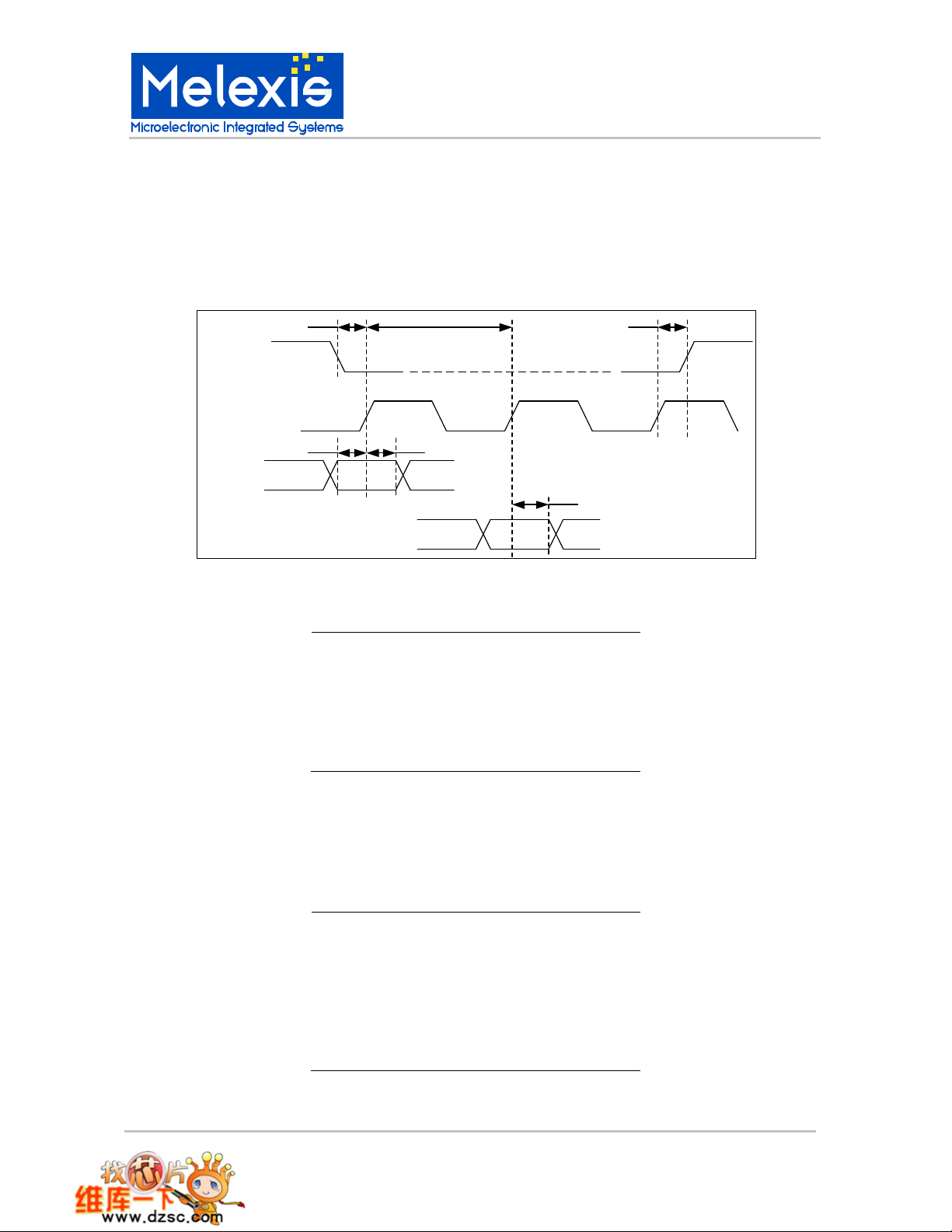
MLX90601 family
IR thermometer modules
the data on SDO starting on the 25th rising edge of the clock (after CS low) as indicated in the figure
above.
Timing/speed
The baud-rate depends on the serial data clock (SCLK) supplied by the master controller and is limited to
125kb/s. The timing requirements are given in the figure and table below
tsclktcls tsch
CS
SCLK
tsu thd
SDI
tdv
SDO
SPI timing
SPI timing requirements
Symbol Parameter Value Unit
tsclk Sclk period min 8
tcls CS low to SCLK high min 50 ns
tsch SCLK low to CS high min 50 ns
tsu data in setup time min 200 ns
thd data in hold time min 200 ns
tdv data out valid min 1
operation codes
The operation code is the first series of 8bits in a command, C[7:0] in the figure on the protocol above.
Below table summarizes the operations available in MLX90313C.
Operation Codes
mnem. C[7:0] Command
WR
RD
WEPR
ER
REPR
BLWR
BLER
X101X0XX
X10010XX
0001XXXX
001XXXXX
X0001XXX
1001XXXX
101XXXXX
Write internal register
Read internal register
Write EEPROM
Erase EEPROM
Read EEPROM
Block Write EEPROM
Block erase EEPROM
µs
µs
3901090601 Page 41 of 49 Aug/02
Rev. 007

MLX90601 family
−=1
2
IR thermometer modules
Temperature registers
The object and ambient temperatures are stored into internal registers.
A table containing the most interesting internal register addresses is included below:
Address list internal registers
Register Function Address
Irout Tobject (lin) 09h
Tout Tambient (lin) 0Ah
These registers keep the linearised object and ambient temperature.
Register format:
Bit 15 14 13 12 11 10 9 8 7 6 5 4 3 2 1 0
Name D11 D10 D9 D8 D7 D6 D5 D4 D3 D2 D1 D0 OVH OVL FE Res
D11..D0 : 12 bit temperature data
OVH: Overflow flag for Tambient measurement, Ta>Tamax, D[11:0] set to FFFh
OVL: Underflow flag for Tambient measurement, Ta<Tamin, D[11:0] set to 000h
FE: Fatal Error in EEPROM.
Res Not used, always zero.
The measured temperature can be obtained from the register content as follows:
Rt
T +−
12
Where:
T measured temperature
Rt register value (12 bit, 0x000 to 0xFFF)
Tmax maximum calibrated temperature
Tmin minimum calibrated temperature
EEPROM reprogramming
Every MLX90601 module has 8 words of 16bits of EEPROM space free to use for the user. One can
freely use this memory space for serialization or storing some other info. Also, in some cases it is
necessary to redefine functionality of the MLX90601 infrared module.
The configuration constants are stored in EEPROM non-volatile memory. Note that also the linearization
constants are stored in EEPROM, and erasing or over-writing these will irreversible destroy the modules’
proper operation. Reprogramming the EEPROM must be done with care.
Here’s how to rewrite a specific EEPROM address.
13. Write 0xB200 to register address 0x10. This unlocks EEPROM control registers. The module now
stops updating it’s output
14. Write 0x0065 to register address 0x18. Enables charge pump for programming.
15. Erase the address you want to rewrite
16. Write the new data in the EEPROM address
17. Repeat steps 3 and 4 for any further programming
18. You now can cycle the power for restarting the chip in normal operation, with new settings
Make sure never to use the Block Write or Block Erase commands, as they completely erase the
EEPROM.
For further details please refer to MLX90313 datasheet.
TminTmin)(Tmax
3901090601 Page 42 of 49 Aug/02
Rev. 007
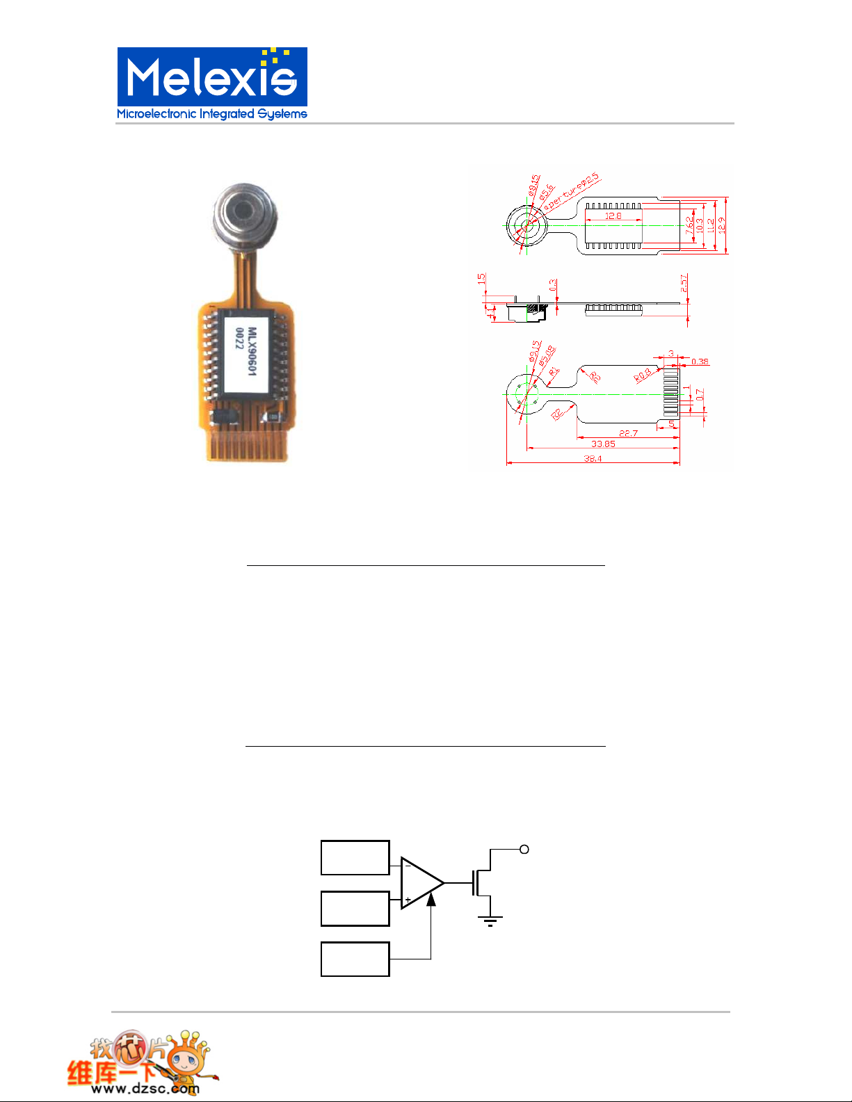
11.4 Physical outline
MLX90601 family
IR thermometer modules
11.5 Pin-out and pin descriptions
pin-out information
pin name function
1 VSS Ground connection
2 REL1 Relay output
3 IROUT PWM coded output infrared
temperature
4 TEMPOUT PWM coded output ambient
temperature
5 VREF Reference voltage output
6 VDD Supply voltage
7 SDIN SPI data in
8 SCLK SPI clock
9 SDOUT SPI data out
10 CSB SPI chip select
VSS Supply pin (0V)
REL1 Open drain relay driver output. The typical on-resistance of this driver is <10
Ohms.
REL1
Tobject
COMP
Threshold in
EEPROM
VSS
Hysteresis
in EEPROM
3901090601 Page 43 of 49 Aug/02
Rev. 007

MLX90601 family
dependent. These settings can be changed by factory programming on request.
IR thermometer modules
The comparator is a digital comparator, with a resolution of 12 bits. By default
the input polarity is inverting. Threshold and hysteresis values are version
Refer to calibration settings for factory preset values.
IROUT IRout PWM coded output pin. The duty cycle of the signal on this pin is a linear
representation of Tobject, the temperature of the object the IR sensor is pointed
at.
TEMPOUT Tempout PWM coded output pin. The duty cycle of the signal on this pin is a
linear representation of Tambient, the temperature of the IR sensor, as
measured by the PTC inside MLX90247.
VREF DAC reference voltage. This voltage must be used if the module is used as a
thermostat using the REL1 comparator with external threshold.
VDD Supply pin
SDIN SPI data input
SCLK SPI clock line
SDOUT SPI data output
CSB SPI chip select. Active low.
11.6 Electrical specifications
Parameter symbol condition min typ max unit
Supply Voltage
Supply voltage range VDD 4.75 5 6 V
Power consumption IDD Ta=25C 5 5.6 mA
outputs IROUT/TEMPOUT
PWM modulator resolution 10 bits
PWM Clock period Tclk 45 50 55
PWM Total period T 92.16 102.4 112.64 ms
Leading buffer time t1 % of T 12.5
Trailing buffer time t5 % of T 12.5
Duty cycle high t2 % of T 0 50 %
Duty cycle low t3 % of T 0 50 %
Error signal t4 % of T 25
Rise time* 10% to 90% of Vh 13.3 100
Fall time* 90% to 10% of Vh 13.3 100
Output voltage high Vh Ihigh=2mA 4 V
Output voltage low Vl Ilow=2mA 1 V
Rel1 open drain relay driver
output impedance Ro 10 Ohms
High voltage protections 32 V
µs
%
%
%
µs
µs
3901090601 Page 44 of 49 Aug/02
Rev. 007

MLX90601 family
IR thermometer modules
11.7 Calibration details
Maximum calibrated object temperature 120°C
Minimum calibrated object temperature -20°C
Object temperature Accuracy ±2°C
Maximum calibrated ambient temperature -20°C
Minimum calibrated ambient temperature 85°C
Ambient temperature Accuracy ±1°C
Response time 500ms
REL1 source Tobject
REL1 polarity (*) Inverting
REL1 threshold 95°C
REL1 hysteresis 5°C
Emissivity 0.99
Note: Comparator polarity:
Inverting: relay switches OFF if temperature is above the threshold.
Non-inverting : relay switches ON if temperature is above the threshold.
11.8 Applications information
Connection of the MLX90601 module into an application is straightforward. The 5V regulated supply
should be connected between pin 6 (VDD) and pin 1 (VSS).
The outputs can be measured relative to VSS at pin 3 (IROUT) for Tobject and pin 4 (TEMPOUT) for
Tambient, e.g. by means of a voltmeter. In an actual application the module outputs can be directly
connected to the A/D inputs of a microcontroller, e.g. as a replacement for a conventional temperature
sensor. When large loading capacitances are to be used, a series resistor may be necessary. Refer to
electrical specifications.
In many applications, the ambient temperature of the sensor is not needed. In this case, pin 2 can simply
be left open.
The REL1 signal can be used as input for a digital I/O or to drive a relay (not shown). In case of a digital
input the microcontroller must have internal pull-up resistors or an external pull-up resistor must be added.
Here of course the microcontroller connection to the SPI interface is purely optional.
IR sensor
Thermisto
MLX90247
IRINP
IR+
IRINN
IR-
r
Rsens
VSS
TINP
TINN
VCM25V
VSS
OPA
OPA
A/D
Digital
A/D D/A
Control and Support Blocks
D/A
Ta
MLX90313
IROUT
TEMPOUT
12
COMP
REL1
VREFP
VDDCREF
SPI
3
4
2
5
6
Application
Microcontroller
Timer input
Timer input (optional)
Vref
5V
VSS
MLX90601
Micro-controller I/O-port
CSB
SDOUT
1019 8
SDIN
SCLK
7SPI
3901090601 Page 45 of 49 Aug/02
Rev. 007

MLX90601 family
IR thermometer modules
12 ESD Precautions
Electronic semiconductor products are sensitive to Electro Static Discharge (ESD).
Always observe Electro Static Discharge control procedures whenever handling semiconductor products.
13 Reliability Information
Melexis devices are classified and qualified regarding suitability for infrared, vapor phase and wave
soldering with usual (63/37 SnPb-) solder (melting point at 183degC).
The following test methods are applied:
• IPC/JEDEC J-STD-020A (issue April 1999)
Moisture/Reflow Sensitivity Classification For Nonhermetic Solid State Surface Mount Devices
• CECC00802 (issue 1994)
Standard Method For The Specification of Surface Mounting Components (SMDs) of Assessed
Quality
• MIL 883 Method 2003 / JEDEC-STD-22 Test Method B102
Solderability
For all soldering technologies deviating from above mentioned standard conditions (regarding peak
temperature, temperature gradient, temperature profile etc) additional classification and qualification tests
have to be agreed upon with Melexis.
The application of Wave Soldering for SMD’s is allowed only after consulting Melexis regarding assurance
of adhesive strength between device and board.
For more information on manufacturability/solderability see quality page at our website:
http://www.melexis.com/
14 FAQ
Q: What is the accuracy?
A: For the standard offered modules the accuracy is ±2°C for the object temperature and ±1°C for
the ambient temperature.
Q: Does accuracy increase when the temperature range is decreased?
A: No. The main error comes from limited measurement precision during calibration. These
imperfections are the same for all modules. High precision calibration can be provided for some custom
products. Please contact Melexis customer support.
Q: What is FOV?
A: The FOV or Field Of View is a definition of the area the sensor is ‘seeing’. The sensor will detect
radiation coming in at an angle, relative to the sensor’s central axis, from 0° to 35°. The full viewing angle
is thus 70°.
Q: What is the useful temperature range?
A: There are two temperature ranges of interest; the temperature of the object (or target), which you
are trying to measure and the temperature of the sensor. The sensor temperature, called Tambient,
should be in the calibrated temperature range. See calibration details. Outside this range the ambient
temperature compensation will no longer work and calculation of the object’s temperature will no longer
be correct. The object temperature, called Tobject, should be between –20°C and 120°C. Outside this
range the IROUT output will saturate.
3901090601 Page 46 of 49 Aug/02
Rev. 007

MLX90601 family
IR thermometer modules
Q: Can the temperature ranges be changed?
A: Yes, MLX90313 is a programmable device. Melexis selected a limited set of standard ranges that
will fit the majority of applications in order to limit delivery times. However, if necessary, the ranges can
be adapted for any particular application. Depending on the application, the user may do so himself using
the EVB board and software. For other applications Melexis may have to do custom calibration. Please
contact Melexis customer support.
Q: Can the Field of View (FOV) be made smaller?
A: In theory, yes. In most cases it is sufficient to place a tube over the sensor, narrowing the opening
angle. After narrowing the FOV, the module will be out of calibration. For applications that require a small
FOV, Melexis can provide custom calibrated devices. Please contact Melexis customer support.
Q: IR radiation is comparable with light. Does my object have to be black?
A: No, the appearance in the visible light spectrum completely differs from the appearance for IR
wavelengths. Water and glass for instance, are completely opaque for IR, and thus you can perfectly
measure the temperature. Air is transparent for IR and does not influence the measurement. The better
name for this property is EMISSIVITY
Q: What is emissivity and how does it affect my measurement?
A: Emissivity is the ratio of the emitted IR energy over the total IR energy that an object has. You
can find the value for this property by searching the internet, material data sheets etc. Ice, water, skin,
clothes, most non-metallic coatings have an emissivity of 0.90 to 0.99. Emissivity should be close to 1.
When measuring objects with low emissivity, reflections of the ambient temperature will come into the
thermopile sensor. Therefore there is a measurement error depending on the difference between object
and ambient temperature. If the surface of the target has an emissivity lower than 0.7, you can still
measure it, but here some tips and tricks are needed. Contact the application engineer for support.
3901090601 Page 47 of 49 Aug/02
Rev. 007
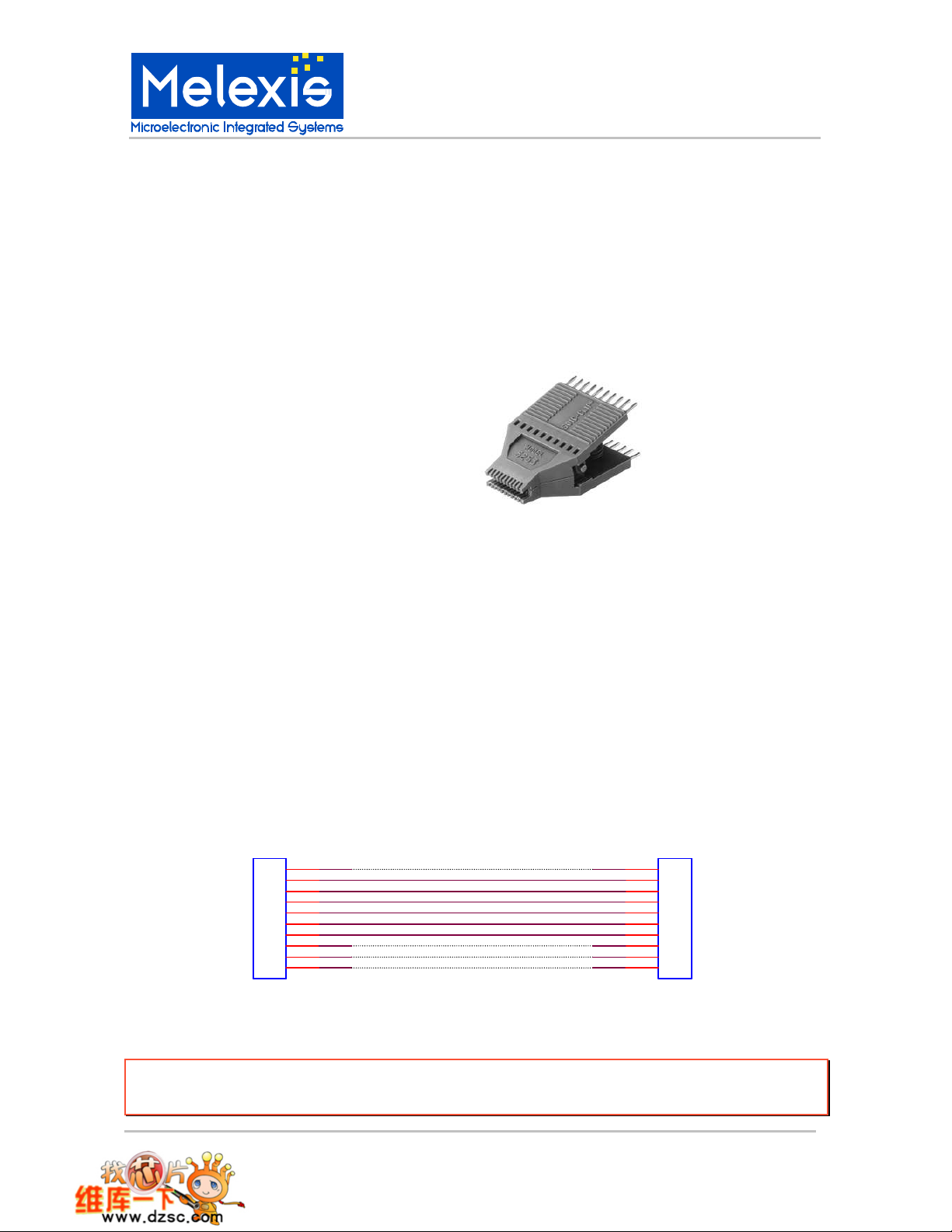
MLX90601 family
IR thermometer modules
15 Appendix A: SPI interfacing to automotive modules
The MLX90601EZA-BAA and MLX90601EZA-DAA do not have a connector with the SPI interface signals.
To communicate with the module, a SOIC clip can be mounted directly onto the back of the 90313 ASIC.
The SOIC clip itself can be connected to the EVB board by means of a flat cable.
Melexis does not supply these cables; references to the components are given below so the user can
build a cable himself.
15.1 Component references
SOIC-20 clip
Manufacturer : Hirschmann
Order code : 933 083-001
Flat cable
10 Conductors, 28 AWG, Stranded, 1mm Pitch, Gray Color, Round Conductor Flat Cable
Manufacturer: 3M
Order code: 3625/10
Connector mating 1mm pitch flat cable and EVB board connector
Manufacturer : 3M
Order code : 3M™ 2mm X 2mm Wire mount Socket, 152210-0100-GB,
or equivalent.
15.2 SPI Communication cable pin-out
SOIC CLIP SIDE
REL1
6
VSS
5
VDD
15
SDIN
8
SDOUT
18
CSB
19
SCLK
17
IROUT
7
VREF
12
TEMPOUT
20
SOIC CLIP
Note: dashed connections are purely optional. They are not necessary to establish SPI communication.
However they may help making measurements.
Attention: when the clip is mounted onto the ASIC, temperature measurement values will be influenced,
and the module may be out of specification. Measured values when using the SOIC test clip must be
interpreted purely indicative.
3901090601 Page 48 of 49 Aug/02
Rev. 007
FLAT CABLE
CONNECTOR
REL1
VSS
VDD
SDIN
SDOUT
CSB
SCLK
IROUT
VREF
TEMPOUT
1
2
3
4
5
6
7
8
9
10
CONN FLEX 10

MLX90601 family
Devices sold by Melexis are covered by the warranty and patent indemnification provisions appearing
press, statutory, implied, or by description regarding
the information set forth herein or regarding the freedom of the described devices from patent
and without
notice. Therefore, prior to designing this product into a system, it is necessary to check with Melexis for
current information. This product is intended for use in normal commercial applications. Applications
nge, unusual environmental requirements, or high reliability
ment are specifically not
urnished by Melexis is believed to be correct and accurate. However, Melexis shall
ages, including but not limited to personal injury,
ness or indirect, special incidental or
quential damages, of any kind, in connection with or arising out of the furnishing, performance or
use of the technical data herein. No obligation or liability to recipient or any third party shall arise or
QS9000, VDA6.1 and ISO14001 Certified
IR thermometer modules
Disclaimer
in its Term of Sale. Melexis makes no warranty, ex
infringement. Melexis reserves the right to change specifications and prices at any time
requiring extended temperature ra
applications, such as military, medical life-support or life-sustaining equip
recommended without additional processing by Melexis for each application.
The information f
not be liable to recipient or any third party for any dam
property damage, loss of profits, loss of use, interrupt of busi
conse
flow out of Melexis’ rendering of technical or other services.
© 2002 Melexis NV. All rights reserved.
For the latest version of this document, go to our website at:
www.melexis.com
Or for additional information contact Melexis Direct:
Europe and Japan: All other locations:
Phone: +32 13 67 04 95 Phone: +1 603 223 2362
E-mail: sales_europe@melexis.com E-mail: sales_usa@melexis.com
3901090601 Page 49 of 49 Aug/02
Rev. 007
 Loading...