

MELEXIS MLX90314ABL Datasheet
MLX902xx Name of Sensor Rev Y.X 22/Aug/98 Page 1
MLX90314AB
Programmable Sensor Interface
MLX90314AB Programmable Sensor Interface Page 1 Rev 2.2 23/Oct/01
Features and Benefits
Microprocessor-controlled signal conditioning for bridge-type sensors
Suited for low-cost sensors: reduction of non-linearity by programmable coefficients
External or internal temperature sensor for compensating temperature errors
Versatile output signal ranges: 4, 5, 10, or 11VDC; 4 to 20 mA loop
Mass calibration easy with 2400 or 9600 baud UART
Power supply from 6 to 35VDC
Applications
Pressure transducers
Accelerometers
Temperature sensor assemblies
Linear position sensors
Ordering Information
art No. Temperature Suffix Package Option Temperature Range
MLX90314AB L LW -40C to 140C
MLX90314AB L UD* -40C to 140C
*UD denotes unpackaged die
Description
The MLX90314AB is a dedicated microcontroller which performs signal conditioning for sensors wired in
bridge or differential configurations. Sensors that can be used include thermistors, strain gauges, load cells,
pressure sensors, accelerometers, etc. The signal conditioning includes gain adjustment, offset control, high
order temperature and linearity compensation. Compensation values are stored in EEPROM and are reprogrammable. Programming is accomplished by using a PC, with an interface circuit (level shifting and glue
logic), and provided software.
The application circuits can provide an
output of an absolute voltage, relative
voltage, or current. The output can be
range limited with defined outputs when
the signal is beyond the programmed
limits. Other features include alarm
outputs and level steering. The robust
electrical design allows the MLX90314AB
to be used where most signal conditioning
and sensor interface circuits cannot be
used. Voltage regulation control is
provided for absolute voltage and current
modes (external FET required).
The standard package is a plastic
SO16W. The device is static-sensitive and
requires ESD precautions.
MLX90314AB
Programmable Sensor Interface
MLX90314AB Programmable Sensor Interface Page 2 Rev 2.2 23/Oct/01
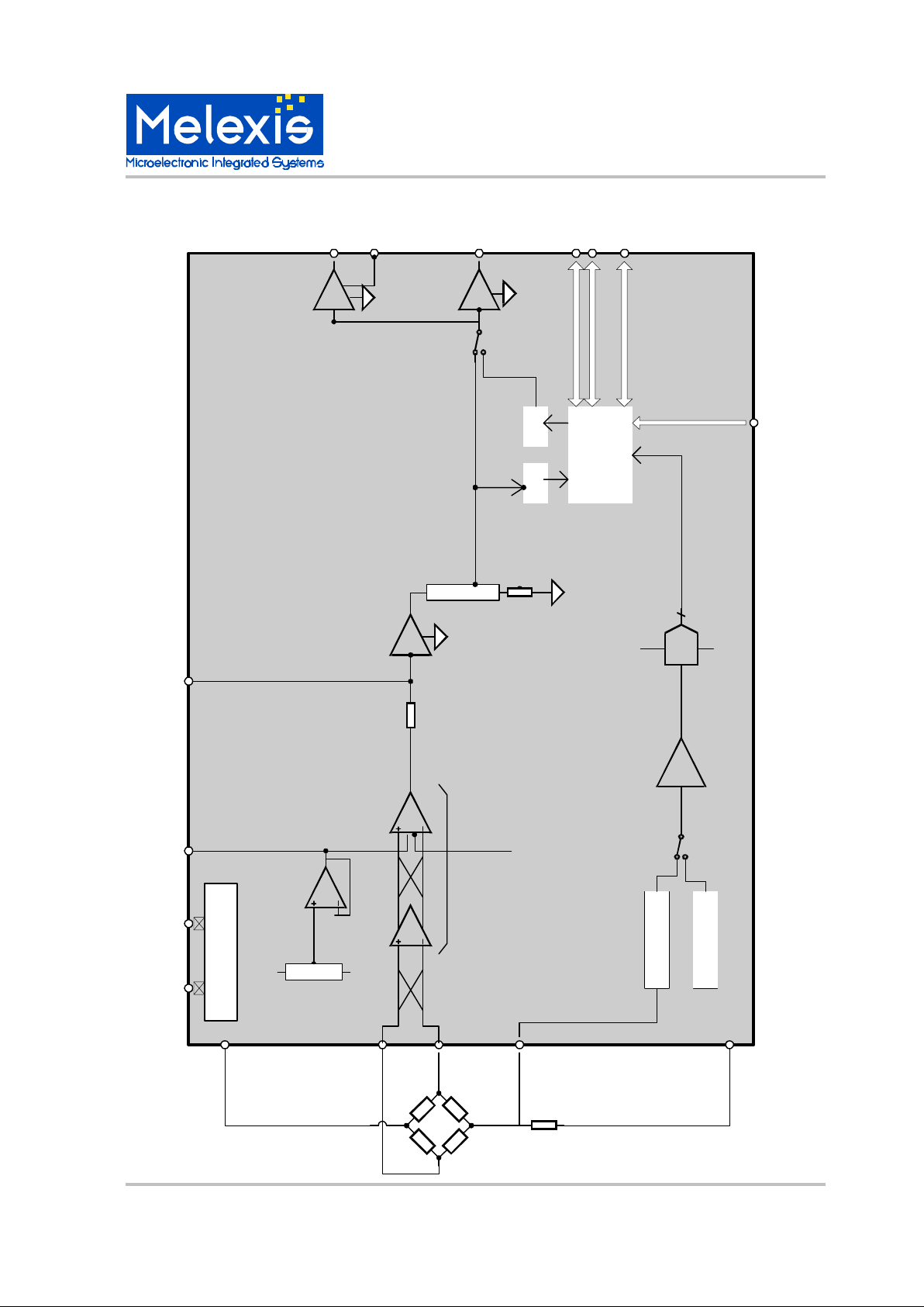
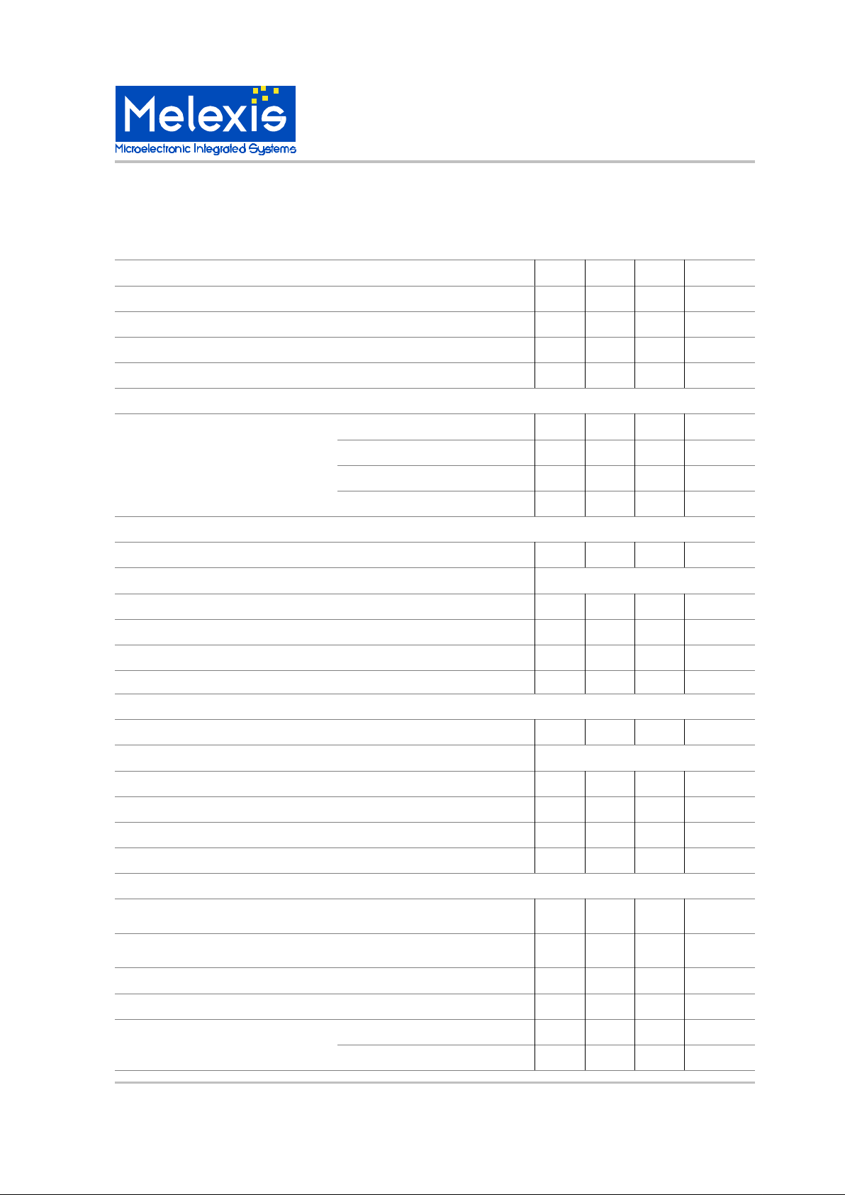
x 35
GAIN
External
Temp Sensor
Internal
Temp Sensor
INV
x2
ADC
3.5V
0V
Temp Amp Gain
GNTP [1:0]
Temperature signal. Used by
microproscessor to perform
temperature linearity corrections.
Hardware Gain = 70
0.97V/V
0.48V/V
1.24kOhm
GAIN
Fine Gain DAC
ADC DAC
Micro-
Processor
Analog
Digital
2-bit
CSGN
1-bit
CSGN
Supply Regulator
VDD
VBP
VBN
TMP
GND
VMO
IO1
IO2
COMS
FLTOFC
OPA
0V
3.5V
DAC_Offset
Coarse Offset
VDD1FET
GAIN
Voltage Mode
Current Mode
CMO
CMN
TSTB
Figure 1.
Functional Block Diagram
MLX902xx Name of Sensor Rev Y.X 22/Aug/98 Page 3
MLX90314AB
Programmable Sensor Interface
MLX90314AB Programmable Sensor Interface Page 3 Rev 2.2 23/Oct/01
Table 1. MLX90314 Electrical Specifications
DC operating parameters: TA = -40 to 140oC, V
DD1
= 6 to 35VDC (unless otherwise specified).
Parameter Symbol Test Conditions Min Typ Max Units
Regulator & Consumption
Input voltage range VIN V
DD1
(Regulator connected) 6 35 V
Supply current IDD @ TA = 100ºC Current Mode 2.1 mA
Supply current IDD @ TA = 100ºC Voltage Mode 5.0 mA
Regulated supply voltage V
REG
4.5 4.75 5.2 V
Regulated voltage
temperature coefficient
-600 uV / ºC
Supply rejection ratio PSRR V
DD1
> 6V 90 dB
Instrumentation Amplifier
Differential input range VBP-VBN IINV = 0 -2.88 8.38 mV/V
(Vdd)
Differential input range VBP-VBN IINV = 1 -8.38 2.88 mV/V
(Vdd)
Common mode input range 1/2(VBP+VBN) 38.0 65.0 %VDD
Pin leakage current Pins VBP & VBN to GND, VDD = 8.0 nA
Common mode rejection CMRR 60 dB
Hardware gain 69 84 V/V
Coarse offset control Range CSOF[1:0] = 00 -4.37 -3.97
mV/V
CSOF[1:0] = 01 -1.46 -1.09
mV/V
CSOF[1:0] = 10 1.09 1.46
mV/V
CSOF[1:0] = 11 3.97 4.37
mV/V
Fixed offset control range High 1.71 2.29
mV/V
Low -2.00 -1.43
mV/V
IA chopper frequency 300 kHz
Gain Stage
Course gain CSGN = 000 3.0 3.3 V/V
(Fixed Gain = 1023)
CSGN = 001 4.9 5.4 V/V
CSGN = 010 8.0 8.8 V/V
CSGN = 011 12.8 14.1 V/V
CSGN = 100*
7.9 8.7
V/V
CSGN = 101* 12.7 14.0 V/V
* CSGN = 100 to 111: voltage mode
only, not applicable to current mode.
Output > 6.5V; MSB = 1
Output < 6.5V; MSB = 0
MLX90314AB
Programmable Sensor Interface
MLX90314AB Programmable Sensor Interface Page 4 Rev 2.2 23/Oct/01
Table 1. MLX90314 Electrical Specifications (continued)
DC operating parameters: TA = -40 to 140oC, V
DD1
= 6 to 35VDC (unless otherwise specified).
Parameter Test Conditions Min Typ Max Units
Coarse gain CSGN = 110* 20.4 23.0 V/V
CSGN = 111* 33.1 36.6 V/V
Fixed gain control range 0.480 0.970 V/V
Digital Mode & Current Mode Coarse Gain Stage
Course Gain CSGN = 00 1.05 1.17 V/V
CSGN = 01 1.71 1.89 V/V
CSGN = 10 2.77 3.06 V/V
CSGN = 11 4.48 4.95 V/V
Output voltage span CSGN[2:2] = 0 4.5 6.5 V
Gain 2.74 3.04 V/V
CSGN[2:2] = 1 6.5 11 V
Gain 7.24 7.86 V/V
Minimum output voltage -0.2 V
Output source current 2.0 mA
Output sink current @ 0V output voltage 20 uA
Output resistance Over complete output range 25 Ohms
Digital mode output span CSGN[2:2] = 0 6.5 V
CSGN[2:2] = 1 11.0 V
Digital mode step size VDD = 5V, CSGN[2:2]=0 6.5 mV
VDD = 5V, CSGN[2:2]=1 11.0 mV
Capacitive load VMO pin 10 nF
Current Mode Output Stage
Fixed gain R
SENSE
= 24 ohm 8.4 9.3 mA/V
Output current CMO pin Current mode 27 mA
Current sense resistor 24 Ohms
Digital mode current output span VDD = 5V 23 mA
Digital mode current step Size VDD = 5V,R
SENSE
=24Ù 30 uA
Signal Path ( General)
Overall gain Voltage mode 98 2100 V/V
Current mode = 24Ù 284 2625 mA/V
Overall non-linearity -0.25 0.25 %
Ratiometry Error (4.75V – 5.25V) Overall Gain < 250V/V -1.75 1.75 %
Overall Gain > 250V/V
-4.6
+4.6
%
Voltage Mode Output Stage ( See Voltage Mode)
MLX902xx Name of Sensor Rev Y.X 22/Aug/98 Page 5
MLX90314AB
Programmable Sensor Interface
MLX90314AB Programmable Sensor Interface Page 5 Rev 2.2 23/Oct/01
Table 1. MLX90314 Electrical Specifications (continued)
DC operating parameters: TA = -40 to 140oC, V
DD1
= 6 to 35VDC (unless otherwise specified).
Parameter Test Conditions Min Typ Max Units
Bandwidth (-3dB) 39 nF connected from FLT to GND 2.8 3.5 4.2 KHz
18.0
mVRMS
Temperature Sensor & - Amplifier
Temperature sensor sensitivity 390 uV/ºC
Temperature sensor output voltage 70 380 mV
Temperature Sensor & Amplifier (continued).
Input voltage range TMP pin GNTP[1,0] = 00 207 517 mV
@ VDD = 5.0V
GNTP[1,0] = 01 145 367 mV
GNTP[1,0] = 10 101 263 mV
GNTP[1,0] = 11 71 186 mV
DAC
Resolution 10 Bit
Monotonicity Guaranteed By Design
Ratiometric output range (DAC output) 1 75 % VDD
Offset Error 10 LSB
Differential non-linearly 1 LSB
Integral non-linearity 2 LSB
ADC
Resolution 10 Bit
Monotonicity
Guaranteed by design
Ratiometric input range 1 75 % VDD
Offset error 10 LSB
Differential non-linearly 1 LSB
Integral non-linearity 2 LSB
On-Chip RC Oscillator and Clock
Untrimmed RC oscillator
frequency
40 250 kHz
Trimmed RC oscillator frequency
(Measured at TMP pin with TSTB pin pulled low after power up)
86.9 87.8 88.7 kHz
Frequency temperature coefficiency 26 Hz/ºC
Clock Stability with temperature compensation over full temperature range -3 +3 %
Ratio of f (microcontroller main clock
and (RC oscillator)
TURBO = 0 7
TURBO = 1 28
Noise, VDD = 5V, C
FLT
=39nF, CL=10nF, RL =5KÙ, Analog Mode (Max. gain)
MLX90314AB
Programmable Sensor Interface
MLX90314AB Programmable Sensor Interface Page 6 Rev 2.2 23/Oct/01
Table 1. MLX90314 Electrical Specifications (continued)
DC operating parameters: TA = -40 to 140oC, V
DD1
= 6 to 35VDC (unless otherwise specified).
Parameter Test Conditions Min Typ Max Units
Input & Output Pins (I01 & I02)
Digital input levels
Low
0.5
V
High VDD-0.5
Output Levels @ output current = 5mA low VDD-0.4 0.4 V
@ Output current = 5mA high VDD
TSTB Pin
Input levels Low 0.5 V
High VDD-0.5
Pull-up Resistor 66 kOhms
FLT Pin
Output resistance 1.24 kOhms
Output voltage range VDD = 5V 0.05 3.6 V
OFC Pin
Output voltage range VDD = 5V 0.05 3.75 V
Load capacitor 20 pf
UART & COMS Pin
UART baud rate TURBO = 0 2400 baud
TURBO = 1 9600 baud
COMS pin input levels Low 0.3*VDD V
High 0.7*VDD V
COMS Pin Output Resistance Low 100 Ohms
High 100 kOhms
MLX902xx Name of Sensor Rev Y.X 22/Aug/98 Page 7
MLX90314AB
Programmable Sensor Interface
MLX90314AB Programmable Sensor Interface Page 7 Rev 2.2 23/Oct/01
Table 2. Absolute Maximum Ratings
Supply voltage (ratiometric) V
DD
Max
6V
Supply voltage (ratiometric) VDD Min
4.5V
Supply voltage (operating), V
DD1
Max 35V
Reverse voltage protection -0.7V
Supply current, Current Mode, IDD 3.5mA
Supply current, Voltage Mode, IDD 4.5mA
Output current, I
VMO
8mA
Output current (short to VDD), I
SCVMO
100mA
Output current (short to VSS), I
SCVMO
8mA
Output voltage, V
VMO
+11V
Power dissipation, PD 71mW
Operating temperature range, T
A
-40 to +140°
Storage temperature range, TS
-55 to +150°C
Maximum junction temperature, TJ 150°C
Unique Features
Customization
Melexis can customize the MLX90314 in both
hardware and firmware for unique requirements.
The hardware design provides 64 bytes of RAM, 3
kbytes of ROM, and 48 bytes of EEPROM for use
by the firmware.
Special Information
The output of the sensor bridge is amplified via
offset and gain amplifiers and then converted to the
correct output signal form in one of the output
stages.
The sensitivity and offset of the analog signal chain
are defined by numbers passed to the DAC
interfaces from the microcontroller core (GN[9:0]
and OF[9:0]). The wide range of bridge offset and
gain is accommodated by means of a 2-bit coarse
adjustment DAC in the offset adjustment (CSOF
[1:0]), and a similar one in the gain adjustment
(CSGN[2:0]). The signal path can be directed
through the processor for digital processing. Two I/
O pins are available for analog inputs or digital
outputs. These pins can be used for alarms on
various points on the analog signal path and built-in
or external temperature values.
Programming and Setup
The MLX90314 needs to have the
compensation coefficients programmed for a
particular bridge sensor to create the sensor
system. Programming the EEPROM involves
some minimal communications interface
circuitry, Melexis’ setup software, and a PC.
The communications interface circuitry is
available in a development board. This circuitry
communicates with the PC via a standard RS232 serial communications port.
Cross Reference
There are no known devices which the MLX
90314AB can replace.
ESD Precautions
Observe standard ESD control procedures for
CMOS semiconductors.
MLX90314AB
Programmable Sensor Interface
MLX90314AB Programmable Sensor Interface Page 8 Rev 2.2 23/Oct/01
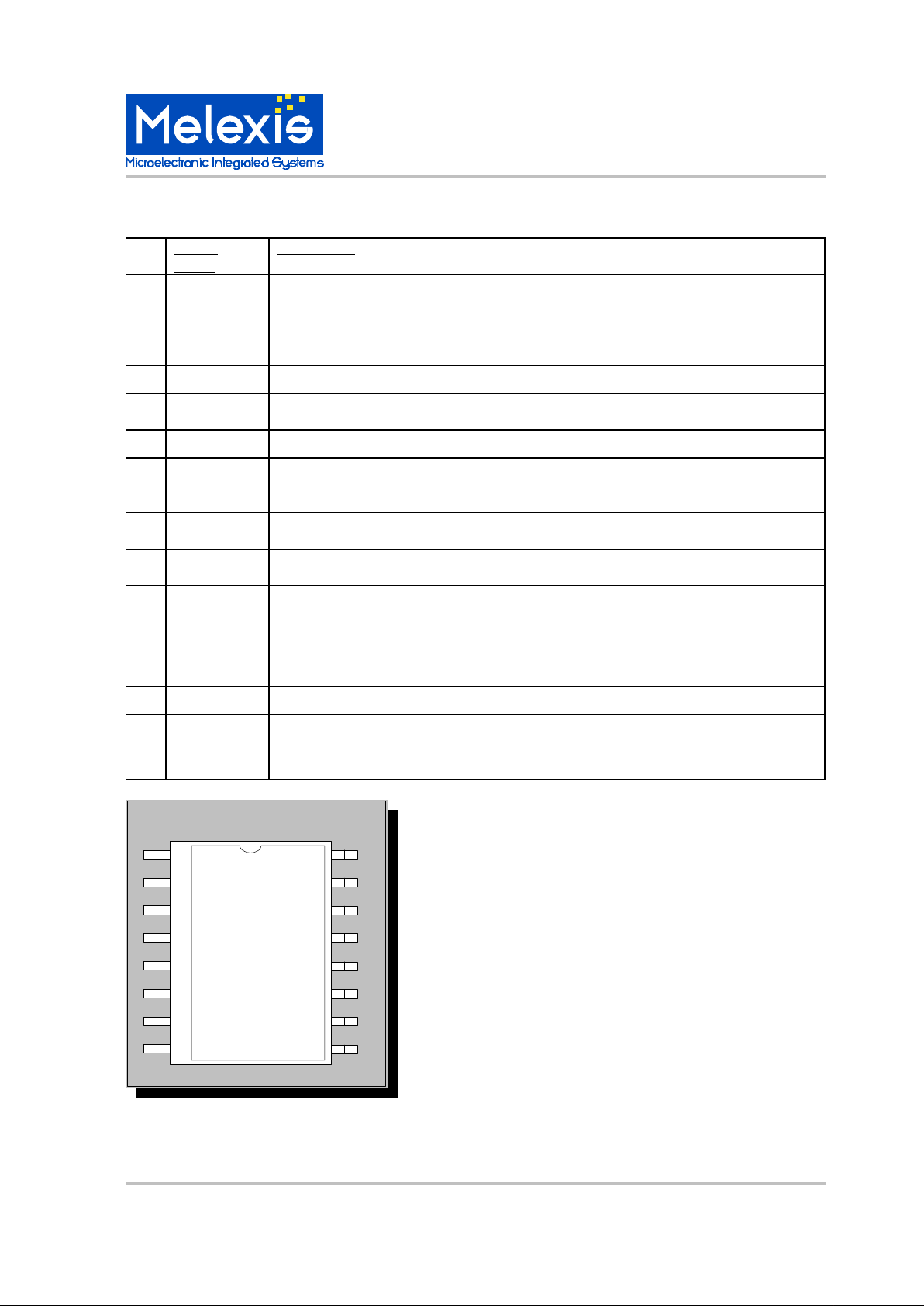
Pin
Signal
Name
Description
1,2 I/O1, 2 Bi-directional I/O. Can also be used as input to A/D converter. I/O can be
controlled by serial communications or by firmware as alarm inputs or level
out. (unconnected when not used)
3 TSTB Test pin for Melexis production testing. (in normal application connected to
VDD)
4 FLT Filter pin; allows for connection of a capacitor to the internal analog path.
5 OFC Offset control output. Provides access to the internal programmed offset
control voltage for use with external circuitry. (unconnected when not used)
6,7 VBN,VBP Bridge inputs, negative and positive.
8 TMP Temperature sensor input. An external temperature sensor can be used in
conjunction with the internal one. The external sensor can provide a
temperature reading at the location of the bridge sensor.
9 VDD Regulated supply voltage. Used for internal analog circuitry to ensure
accurate and stable signal manipulation.
10 FET Regulator FET gate control. For generating a stable supply for the bridge
sensor and internal analog circuitry (generates regulated voltage for VDD).
11 V
DD1
Unregulated supply voltage. Used for digital circuitry and to generate FET
output.
12 VMO Voltage mode output. Compensated sensor output voltage.
13 CMO Current mode output. Compensated sensor output for current mode
operation.
14 CMN Current mode negative rail. Current mode return path.
15 GND Power supply return.
16 COMS Serial communications pin. Bi-directional serial communication signal for
reading and writing to the EEPROM.
Table 3. Pin Description
1
2
3
4
5
6
7
8 9
10
11
12
13
14
15
16
IO1
IO2
TSTB
FLT
OFC
VBN
VBP
TMP
COMS
GND
CMN
CMO
VMO
VDD1
FET
VDD
Figure 2. Pinout (SO16W (LW) Package)
 Loading...