

MELEXIS MLX90255AB Datasheet
MLX90255AA Optical Array Page 1 March 2000
MLX 90255AB Optical array
1. FEATURES
• 128 x 1 Sensor-Element Organization (1 Not Connected, 1 dummy, 128 real, 1 dummy and 1 Dark Pixel)
• 385 Dots-Per-Inch (DPI) Sensor Pitch
• High Linearity and Uniformity for 256 Gray-Scale (8-Bit) Applications
• Optimization: less Gain in order to get better Signal To Noise behavior: up to 13 bits
• Output becomes high impedance after CLK 132
• Extremely low integration times possible: up to 10 µs! (independent of clock speed)
• Output Referenced to Ground
• Low Image Lag ... 0.5% Typ
• Single 5-V Supply
• Replacement of Texas Instruments TSL1301 & TSL1401
• Operation to 1MHz
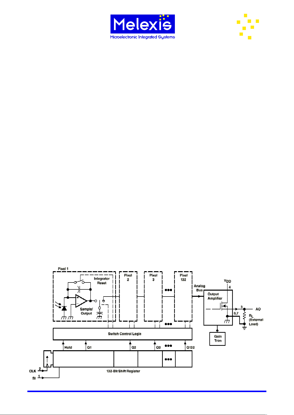
The MLX90255 linear sensor array consists of a 128 × 1 array of photodiodes, associated charge amplifier
circuitry, and a pixel data-hold function that provides simultaneous-integration start and stop times for all
pixels.
The pixels measure 200µm (H) by 66µm (W) and 8 µm spacing between pixels. Operation is simplified by
internal control logic that requires only a serial-input (SI) signal and a clock.
MLX90255AA Optical Array Page 2 March 2000
Detailed description
The sensor consists of 128 photodiodes arranged in a linear array. Light energy falling on a photodiode
generates photocurrent, which is integrated by the active integration circuitry associated with that pixel.
During the integration period, a sampling capacitor connects to the output of the integrator through an analog
switch. The amount of charge accumulated at each pixel is directly proportional to the light intensity and the
integration time. The output and reset of the integrators is controlled by a 132-bit shift register and reset
logic. An output cycle is initiated by clocking in a logic 1 on SI. This causes all 132 sampling capacitors to be
disconnected from their respective integrators and starts an integrator reset period. As the SI pulse is
clocked through the shift register, the charge stored on the sampling capacitors is sequentially connected to
a charge-coupled output amplifier that generates a voltage on analog output AO. Two dummy pixel values
are shifted out first, then the 128 actual pixel bits, followed by two additional dummy pixel bits, for a total of
132 data bits.
The integrator-reset period ends 132 clock cycles after the SI pulse is clocked in. So the light integration
starts after the 132
nd
CLK pulse. The light integration ends at the next SI pulse. Between the end of the
132nd clock pulse and the next SI pulse, a minimum time of 10µs is necessary for an effective S&H function.
So the minimum integration time for the MLX90255AB is 10µs.
The AO is driven by a source follower that requires an external pulldown resistor. (typically 330ohm) After the
132
nd
CLK pulse, the output becomes high impendance.
The output is nominally 125mV for no light input and 2.4V for a nominal full-scale output. There is no cosine
compensation: all 132 pixels have the same gain.
The MLX90255 is intended for use in a wide variety of applications, including: image scanning, mark and
code reading, optical character recognition (OCR) and contact imaging, edge detection and positioning, and
optical linear and rotary encoding. The MLX90255 is a replacement for the Texas Instruments' TSL1301 and
TSL1401 parts.
Timing Waveform
CLK
minimal 10µs
SI
Internal
reset
integration
AO
132 Clock Cycles
Not Integrating
Integrating
2+128+2 clock cycles
high impedance
MLX90255AA Optical Array Page 3 March 2000
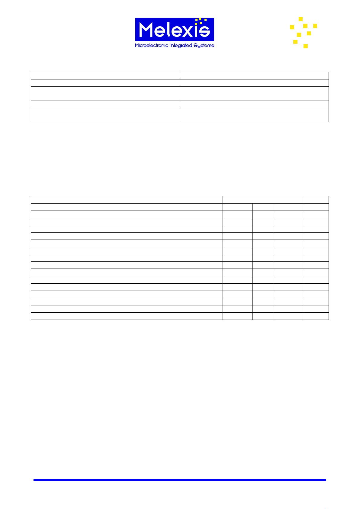
2. ABSOLUTE MAXIMUM RATINGS
Supply Voltage, Vdd +7V
Digital input current range -20 to 20 mA
Operating free-air temperature range, Ta -40degC to +125degC
(automotive compliant optical package)
Storage temperature range, Tstg -40degC to +125degC
Lead temperature
1,6 mm (1/16 inch) from case for 10 seconds
260degC
Stresses beyond those listed under "absolute maximum ratings" may cause permanent damage to the
device.
These are stress ratings only, and functional operation of the device at these or any other conditions beyond
those indicated under "recommended operating conditions" is not implied.
Exposure to absolute-maximum-rated conditions for extended periods may affect device reliability.
3. ELECTRICAL CHARACTERISTICS
Characteristics Limits Unit
Min Typ Max
Supply voltage Vdd 4.5 5 5.5 V
Input voltage, Vi 0 Vdd V
High-level input voltage, Vih Vdd*0.7 Vdd V
Low-level input voltage, Vil 0 Vdd*0.3 V
Wavelength of light source 400 1000 nm
Clock frequency, Fclock 5 1000 kHz
Sensor integration time below 60degC, Tint (1) 0.01 100 ms
Sensor integration time full Temperature range, Tint (2) 0.01 2 ms
Pixel Charge Transfer Time (full Temp range), Tqt 8
µs
Setup time, serial input, Tsu(si) 100 ns
Hold time, serial input, Th(si) (3) 20 ns
Operating free-air temperature, Tamb -40 +125 DegC
Clock Pulse Duration (high), Tw (H) 320 ns
Clock Pulse Duration (low), Tw (L) 320 ns
(1): we reset till clock pulse 132 (on declining flank)
Ö minimum integration time = (132 – 132)*CLK period + 10 µs (this is the time the S&H cap need to follow)
Ö the minimum integration time becomes 0.01ms, independent of clock speed
(2): at 125degC, the integration time should be limited to 2ms
(3): the SI pulse must go low before the rising edge of the next clock pulse
 Loading...