

MELEXIS MLX90215L, MLX90215E Datasheet
*Patent Pending
MLX90215 Programmable Hall Effect Sensor Rev 4.3 7/6/01 Page 1
MLX90215
Precision Programmable*
Linear Hall Effect Sensor
Description
The MLX90215 is a Programmable Linear Hall Effect
sensor IC fabricated utilizing silicon-CMOS
technology. It possesses active error correction
circuitry which virtually eliminates the offset errors
normally associated with analog Hall Effect devices.
All magnetic response functions of the MLX90215 are
fully programmable for even greater versatility. The
VOQ (V
OUT
@ B=0), sensitivity, direction of slope and
the magnitude of sensitivity drift over temperature, are
all programmable.
The ratiometric output voltage is proportional to the
supply voltage. When using the supply voltage as a
reference for an A/D converter, fluctuations of +10%
in supply voltage will not affect accuracy. When
programmed for a conventional sensitivity (with a
positive gain) , the voltage at the output will increase as
a South magnetic field is applied to the branded face of
the MLX90215. Conversely, the voltage output will
decrease in the presence of a North magnetic field. The
MLX90215 has a sensitivity drift of less than +1%
error, and VOQ stability drift of less than +0.4% error,
over a broad temperature range.
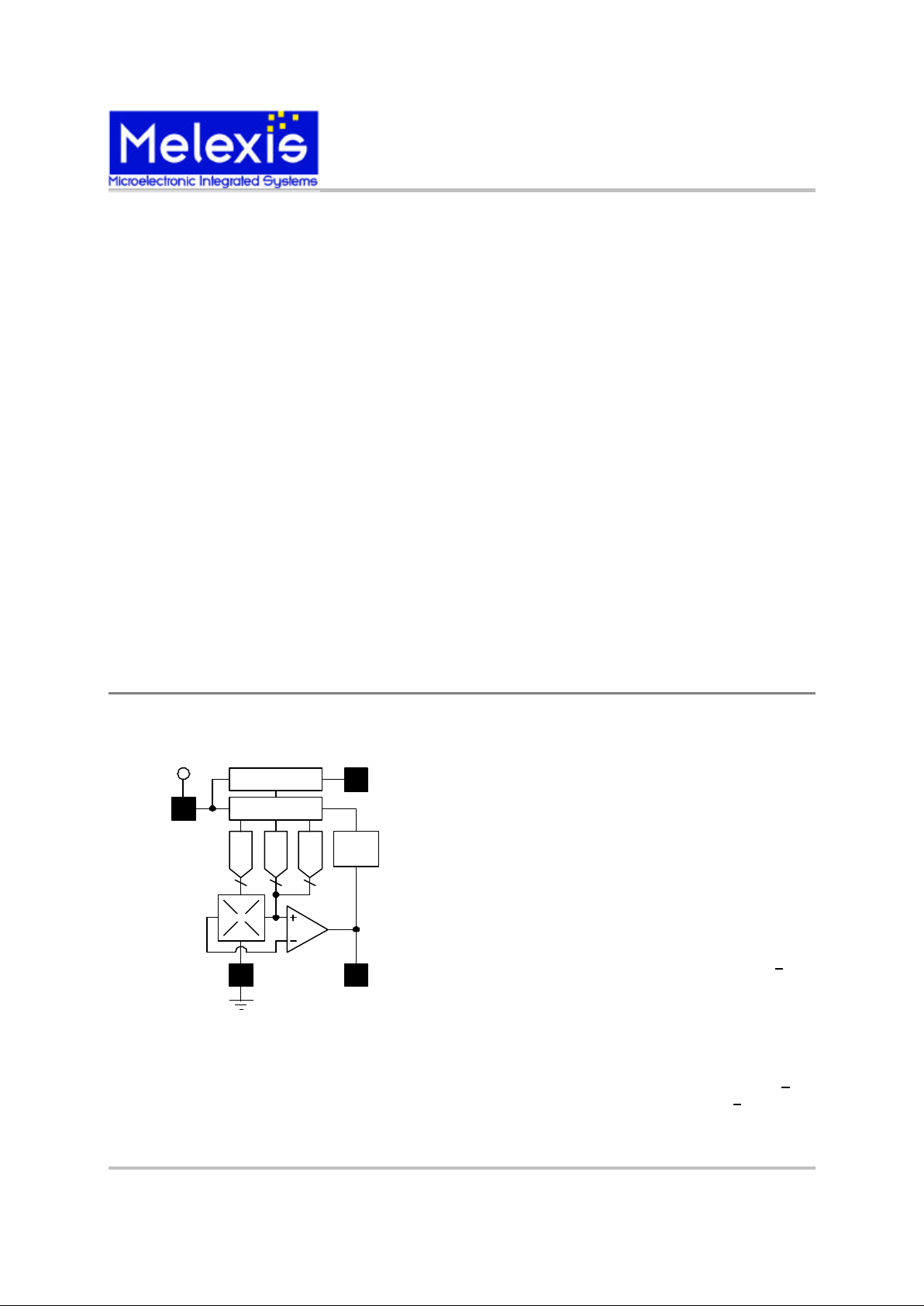
Functional Diagram
Features and Benefits
• Programmable Linear Hall IC
• Quad Switched / Chopper Stabilized
• Ratiometric Output for A/D Interface
• Adjustable Quiescent Voltage (V
OQ
)
• Very Low Quiescent Voltage Temperature Drift
• Adjustable Sensitivity
• Adjustable Temperature Compensation of Sensitivity
Applications
• Linear Position Sensing
• Rotary Position Sensing
• Current Sensing
Ordering Information
Part No. Temperature Suffix Package Temperature Range
MLX90215 L VA(4 Lead SIP) -40°C to 150°C
MLX90215 E VA(4 Lead SIP) -40°C to 85°C
Chopper
Shift Register (RAM)
OTPROM (ROM)
Program
Decoder
1
3
V
DD
2
4
DAC
DAC
DAC
Hall Plate
Pin 1 - VDD (Supply)
Pin 2 - Test/Readback Enable
Pin 3 - VSS (Ground)
Pin 4 - Output
Note: Static sensitive device, please observe ESD precautions.

*Patent Pending
MLX90215 Programmable Hall Effect Sensor Rev 4.3 7/6/01 Page 2
MLX90215
Precision Programmable*
Linear Hall Effect Sensor
Parameter Symbol Test Conditions Min Typ Max Units
Supply Voltage VDD Operating 4.5 5.0 5.5 V
Supply Current IDD B = 0, VDD = 5V, I
OUT
= 0 2.5 4.0 6.5 mA
Output Current
(1)
I
OUT
VDD = 5V + 10% -2 - 2 mA
Quiescent Output Voltage
(2)
VOQ 10-Bit Programmable, B = 0 0.5 - 4.5 V
Output Voltage
(1)
VOH V
DD
= 5V, I
OUT
= -2mA 4.50 4.65 V
Bandwidth
(3)
BW RoughGain @ Min - 1.300 kHz
Bandwidth
(3)
BW RoughGain @ Max 0.130 - kHz
Impulse Response Time
(6)
T
RMIN
RoughGain @ Min 25 - µs
Impulse Response Time
(6)
T
RMIN
RoughGain @ Max 250 µs
Offset Voltage Adjustment
Resolution
∆VOQ B = 0, TA = 25oC -1.5 - 1.5 mV
Offset Voltage Drift
over Temperature
∆VOQ/∆T B = 0, TA = -40oC to 150oC
S < 100mV/mT & VOQ > 0.75V
-20 - 20 mV
Offset Voltage Drift
(2)
over Temperature
∆VOQ/∆T B = 0, TA = -40oC to 150oC
S > 100mV/mT & VOQ < 0.75V
-40 - 40 mV
Range of Sensitivity
(7)
s 13-Bit Programmable 5 - 140 mV/mT
Peak to Peak Noise
(4)
8 25 60 mV
Output Resistance R
OUT
6 Ω
Sensitivity Drift
(5)
TA = 25oC -1 - 1 %
MLX90215 Electrical Specifications
Output Voltage
(1)
VOL VDD = 5V, I
OUT
= 2mA 0.35 0.50 V
Sampling Rate f
SAMP
RoughGain @ Max and Min 4 - 40 kHz
Melexis Inc. reserves the right to make changes without further notice to any products herein to improve reliability, function, or design. Melexis does
not assume any liability arising from the use of any product or application of any product or circuit described herein.
Notes:
(1) If output current and voltage specifications are exceeded, linearity will be degraded.
(2) If VOQ is programmed beyond these limits, the temperature compensation may become a problem at high temperatures. It is not recommended to program values of VOQ below 1V or above 4V when sensitivity exceeds 100
mV/mT. Temperature instability can occur on some devices under these conditions.
(3) Bandwidth is inversely proportional to ROUGHGAIN.
(4) Peak to Peak Noise is a function of ROUGHGAIN setting. See page 5, Peak to Peak Noise versus Sensitivity.
(5) Sensitivity drift is indepe ndent of other parameters and does not include individual tolerances (∆V
OQ
or ∆VOQ/∆T).
The tolerance for sensitivity is + 1% of its initial value. This does not include tolerance stack-up.
(6) If the impulse occurs in the middle of a sample interval, the small signal response delay will double. If a 50% to
100% impulse, slew rate may result in double or triple delay.
(7) 1 mT = 10 Gauss
*Patent Pending
MLX90215 Programmable Hall Effect Sensor Rev 4.3 7/6/01 Page 3
MLX90215
Precision Programmable*
Linear Hall Effect Sensor
How does it Work?
The MLX90215 programming is done through the
output pin, by changing supply voltage levels. Please
note that the VDD is raised to approximately 13V and
18V during programming. Any connected
components must also tolerate this voltage
excursion. When the supply voltage is at 4.5V to
5.5V, the output behaves normally. If the supply
voltage is raised to 13V, the output then behaves as an
input, or LOAD mode, allowing the 31 -bit word to be
clocked in. All data is loaded through a single line,
with no dedicated clock signal. Clock and data are
integrated into one signal which is initiated with the
beginning of the LOAD sequence, then clocked with
the positive edge of each bit. Variables are changed
with the PC software and loaded into the te mporary
register of the device (RAM) via the timings of the
programmer’s microcontroller. Data can be loaded as
many times as desired while in LOAD mode. Once a
word is loaded, results are checked by observing the
output voltage. This can be done with an external
Voltmeter attached directly to pin 4 of the device, or
with the internal ADC of the programmer. Once the
desired program is loaded, the word can be “Zapped”
permanently into ROM.
This is done when the supply voltage rises above 18V,
or ZAP mode, creating enough current to “Zap” 31
zener diodes which correspond to the temporary
register. The ZAP function is a one-time function and
cannot be erased.
The above description is only for reference. The
voltage levels and data transfer rates are completely
controlled by the ASIC programmer. For more
information on the programmer hardware, contact
Melexis and request a datasheet for the SDAP
programmer.
Programming The Quiescent Offset Voltage (VOQ)
10 bits, 1024 steps of resolution, are allotted to adjust
the Quiescent Offset Voltage (VOQ). By utilizing the
HALFVDD function, the VOQ can be set to one of two
ranges. With the HALFVDD function disabled, the
VOQ can be programmed within a range of 10% to 90%
VDD with about 5mV per step resolution. With the
HALFVDD function enabled, the device may be
programmed within a 2V to 3V window with less than
1mV per step resolution
Programming the Sensitivity (Gain)
The sensitivity is programmed with a ROUGHGAIN
and a FINEGAIN adjustment. The ROUGHGAIN is
adjusted by utilizing three bits, or 8 increments. The
FINEGAIN is programmed with 10 bits or 1024
increments. The sensitivity can be programmed within
a range of 5mV/mT to 140mV/mT. Another 1-bit
function allows the direction of the sensitivity to be
reversed. The INVERTSLOPE function, when
activated, will cause the Voltage output of the
MLX90215 to decrease in the presence of a South
magnetic field, and to increase in the presence of a
North magnetic field. Table 2 expresses examples of
sensitivity resulting from programming ROUGH
GAIN and FINE GAIN codes, with the INVERT
SLOPE function turned off.
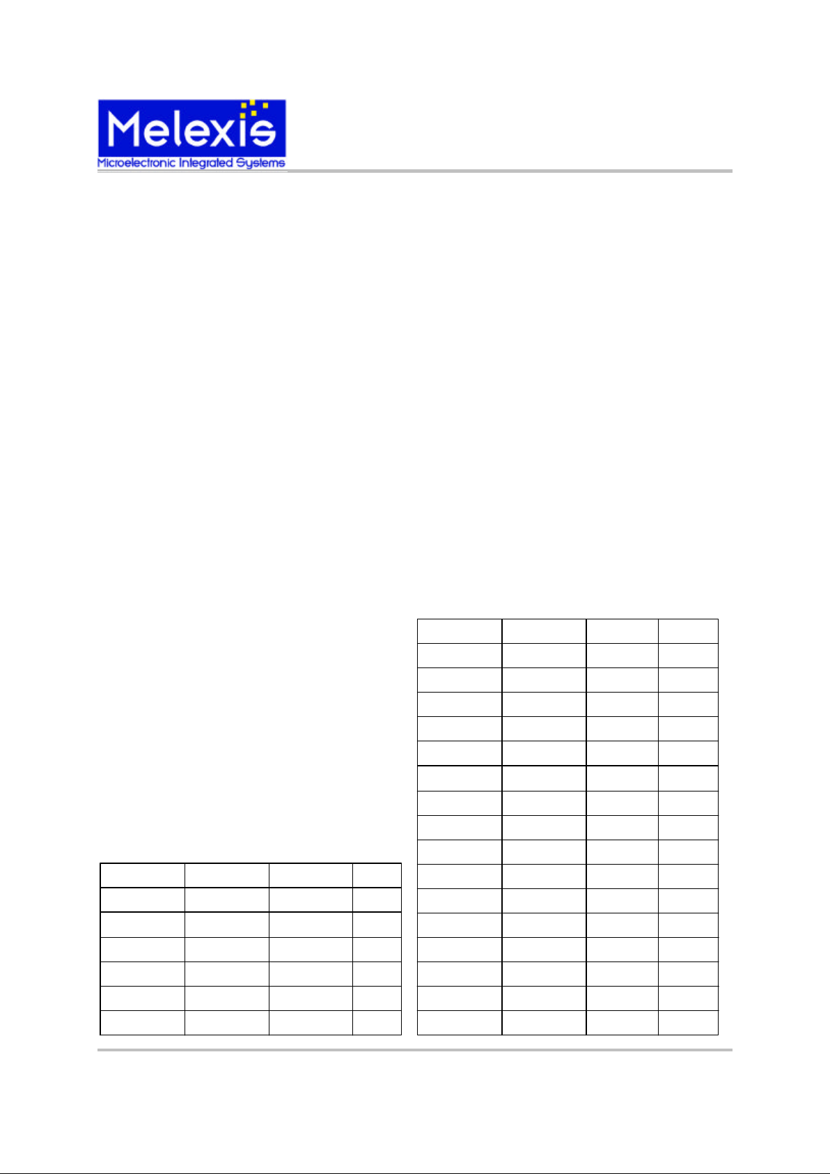
Note: Tables 1 and 2 are examples how various codes affect the
UnitsHalfVDD OffsetDAC Output
0
0
0
1
1
1
0
512
1023
0
512
1023
4.97
2.47
0.03
3.07
2.45
1.83
V
V
V
V
V
V
Table 1 - Programming Offset Voltage (VOQ)
RoughGain FineGain Output Units
0
0
1
1
2
2
0
1023
1023
0
4.1
9.4
6.2
14.6
9.5
22.4
mV/mT
Table 2 - Programming Sensitivity
mV/mT
mV/mT
mV/mT
mV/mT
mV/mT
3
3
4
4
5
5
0
1023
1023
0
14.2
33.1
21.5
50.4
31.3
72.5
mV/mT
mV/mT
mV/mT
mV/mT
mV/mT
mV/mT
6
6
46.2
107
mV/mT
mV/mT
7
7
68.9
140
mV/mT
mV/mT
0
1023
0
1023
0
1023
0
1023
 Loading...