MELEXIS MLX90109 Datasheet

MLX90109
125kHz RFID Integrated Transceiver
Features and Benefits
- Highly Integrated transmitter-receiver for 125kHz ASK transponders
- Parallel antenna gives factor of Qreader improved power efficiency over serial antenna
implementations
- Minimum reader PCB size with SO8 reader IC and minimum external components
- Integrated hardwired decoding for Biphase and Manchester ASK, 2kbit and 4kbit
transponders.
- Direct amplitude modulation on the reader antenna for downlink to transponder.
- Power down mode with Brown out protection
- Optimized system cost
- Fast design-in, ease of implementation.
Applications
Car Immobilizers, portable readers, battery powered door locks, house held appliances, …
Ordering Information
Part No. Temperature Range Package
MLX90109 25oC SO: 150mils 8pins SOIC
-40oC to 85oC
Production parts available Q1 2001
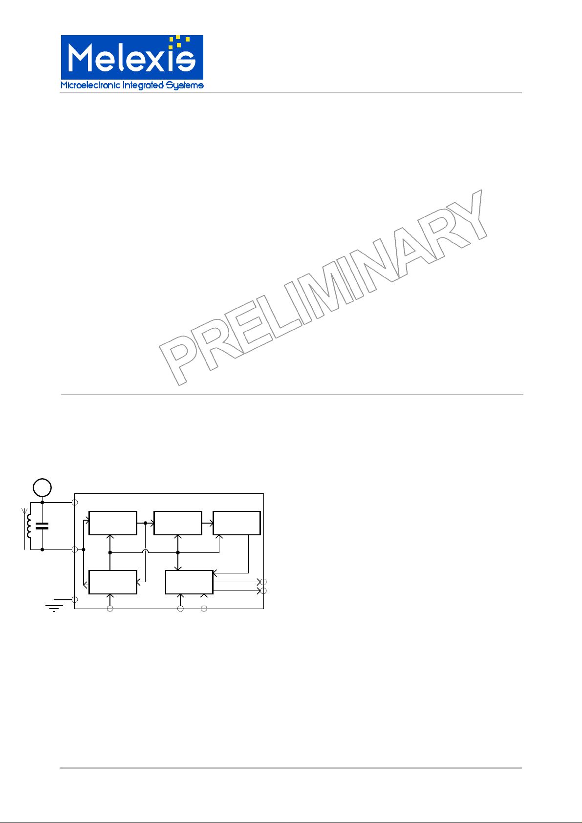
Functional Diagram Description
The MLX90109 is a single chip inductive RFID
transmitter-receiver for the 125kHz range. It has
VDD
VDD
COIL
GND
Peak Det. SC filt
Clock
Loop Gain+
Osc.
MODU SPEED MODE
Digital
demod.
MLX90109
Comparator
Dataout
Clockout
DATA
CLOCK
been conceived for minimum system cost, and
minimum power consumption, whilst offering all
required flexibility for a state of the art AM ReadWrite base station.
An external L and C are connected as a parallel
resonant circuit, which will determine the carrier
frequency and the oscillator frequency of the
reader. This eliminates zero modulation effects,
and avoids the need for an external oscillator.
The antenna amplitude can be adjusted
externally on the fly. This allows straightforward
modulation of the antenna amplitude to write to
the transponder.
The reader IC can easily be switched to power
down by switching the antenna amplitude to
zero.
The MLX90109 can be configured to decode the
transponder signal on-chip. In this case the
decoded signal is available through a 2-wire
interface of clock and data. For minimum
interface wiring, the undecoded transponder
signal can also be made available on a single
wire interface.
MLX90109 Parallel Resonant transceiver Page 1 of 9 Rev 1.4 19-Dec-00

MLX90109
125kHz RFID Integrated Transceiver
MLX90109 Electrical Specifications
DC Operating Parameters TA = -40oC to 85oC, VDD = 5V (unless otherwise specified)
General test conditions (see test set up blockdiagram) Creader= 21pF, Qreader=17, Lreader =75uH, Zant=1kOhm
T: 100% tested, C: guaranteed by Design & Characterization
Parameter Symbol Test Conditions Min Typ Max Units
Supply Voltage VDD 4.5 5 5.5 V T
Operating Resonance Freq. Fres 100 150 kHz C
Fres Temperature detuning
Quality factor Antenna Qant See footnote
∆(T)Fres
1
Antenna Impedance Zant 1 10
-1 +1 % T
10 50 C
kΩ
Power down Current IDDsleep MODU = 5V 1 uA T
Max. Operating Current IDDmax MODU = 1V, excluding antenna driver
0.6 1.5 mA T
current
Coil pin clamping Voltage Vclamp 21 26 V T
Max Antenna Driver Current Idrivemax DC equivalent, See footnote
MODU power up current Imodupor See footnote
MODU power down voltage Vmodupd See footnote
MODU minimum voltage Vmodumin See footnote
3
4
5
2
5 8.5 mA C
60 uA C
4.2 4.35 4.5 V C
0.8 V C
Max. Antenna Voltage swing Vantmax MODU = 1V 8.0 8.6 Vpp T
Modulation depth
1
A minimum Quality factor is required in order for the reader to recover the transponder signal. The maximum
∆Vant
MODU switched between 0.5 and 1.5V, 1.4 2 2.6 V T
quality factor is not limited, since the transponder signal is picked up even.
C
2
Antenna driver current is dimensioned, so as to guarantee that for Zant, within the specified range, the antenna
driver can act as a perfect current source to drive the resonant circuit.
For a typical Zant~ωL*Q = 1kOhm (e.g. L= 67uH, Q=19), and MODU at 1V, MLX90109 will force 4V antenna
amplitude, therefore should supply 4mA current amplitude on the first harmonic sine wave.
Duty cycle is 50%, therefore the equivalent DC current consumption for such a system is 1.3mA.
3
Power up is realized by forcing a current into MODU through the external correction network. This will release
an internal strap to VDD of the MODU pin.
4
The MLX90109 goes in power down mode when the MODU pin is brought to VDD.
5
Voltages below Vmodumin, may cause the antenna Voltage to drop below VSS+0.3V. This will degrade the
performance of the current driver. There is always a slight overshoot of the antenna voltage due to the antenna
resonance.
6
Since the modulation is realized by altering (∆duty )the duty cycle around the 50% value, the driver current
setting influences directly the modulation depth, as Moddepth=Zant*Idrive*∆duty.
MLX90109 Parallel Resonant transceiver Page 2 of 9 Rev 1.4 19-Dec-00

MLX90109
125kHz RFID Integrated Transceiver
See footnote
Modulation depth range See footnote
6
7
68 % C
White Noise rejection Schmitt trigger hysteresis 5 3 mV C
Sensitivity Vsens
40 3 mV T
Filter Gain 28 dB C
Filter ripple 3 dB C
Filter 3db BW slow SPEED = 1 400 – 3.6k Hz C
Filter 3db BW fast SPEED = 0 800 - 7.2k Hz C
Output voltage DATA and
Vout Isink = 2.5mA 0.4 V C
CLOCK pin
Start up time MODU = 5V to 1V 8 ms C
AM demodulation Delay time
0 us C
MODU-IN ANTENNA-OUT
AM demodulation Delay time
Antenna input to Data output
2kHz square wave modulation
Falling edge on antenna
25 periods C
MODE= floating (See footnote 8)
AM demodulation Delay time
Antenna input to Data output
2kHz square wave modulation
Rising edge on antenna
29 periods C
MODE= floating (See footnote 8)
Modulation pulse width
deviation Antenna input to
Data output
Antenna pulse width versus output pulse
width.
MODE= floating (See footnote 8)
-4 0 +4 periods C
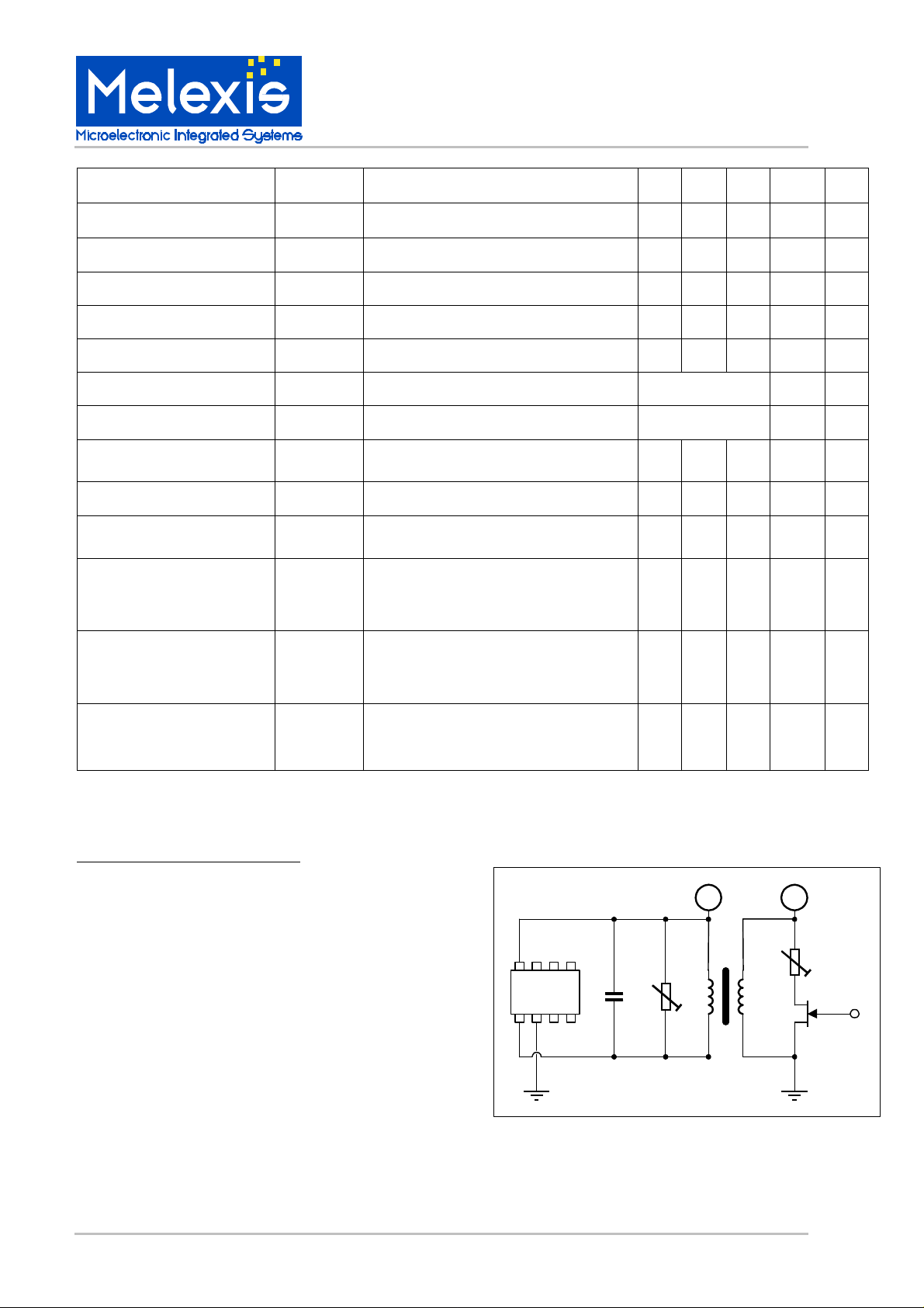
Test set up Block diagram
7
Modulation on the reader antenna is limited towards
maximum modulation depth, to prevent the reader from
VDD
going into power down.
Modudepth = (VPPmax-VPPmin)/( VPPmax+VPPmin)
Since Vppmin (Vmodu=4.2V)=1.6V,
and Vppmax (Vmodu=0.8V)=8.4, modudepthmax=68%.
8
The data slicer samples every 4 clock periods(=1/Fres),
8
7 6 5
90109
1 2 3 4
therefore any pulse on the output can be 4 periods off.
C
R
R
L
par
R
MLX90109 Parallel Resonant transceiver Page 3 of 9 Rev 1.4 19-Dec-00
VDD
L
tag
R
damp
 Loading...