

Page 1
MLX75305
2 - OUT
1 - Vss
3 - Vdd
E
e
VDD
Vref
Light-to-Voltage SensorEyeC
1. Features and Benefits
Converts light intensity to voltage
High linearity
Low temperature dependency
Supply voltage range 3V to 5.5V
Open drain output voltage output
Automotive Cavity SO8 package
Designed for automotive applications
Solder reflow 260degC, MSL3
Automotive qualified AEC-Q100 Grade 1
Operating temperature -40 up to 125degC
RoHS compliant lead-free
2. Application Examples
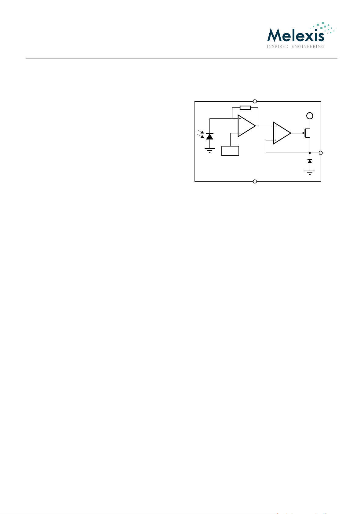
3. Functional Diagram
Figure 1
4. General Description
General
Ambient Light Sensor
LCD Backlight Sensor
LED Power Monitoring
Automotive
Automatic light dimming of instrument
panels and displays
Electrochrome Dimming
Headlights on/off control
Printers/Copiers
Paper feed detection
Paper size and orientation detection
Toner cartridge presence detection
The Melexis SensorEyeC series are CMOS
integrated optical sensor ICs including
photodiode, transimpedance amplifier and output
transistor on one chip. These sensors are designed
for high-volume automotive and non-automotive
applications.
The MLX75305 Light-to-Voltage SensorEyeC
converts ambient or LED light intensity into an
output voltage.
The MLX75305 block diagram is shown above and
contains following blocks: a photodiode, a
transimpedance amplifier to convert and amplify
the photocurrent of the photodiode and an open
drain output buffer stage.
REVISION 9 - OCTOBER 17, 2016
[390107530501]
Page 2
MLX75305
REVISION 9 - OCTOBER 17, 2016
Product
Temperature
Package
Option Code
Packing Form
MLX75305
K (-40°C to 125°C)
XD
AAA-000
RE
MLX75305
K (-40°C to 125°C)
XD
ABA-000
RE
Temperature Code:
K for Temperature Range -40°C to 125°C
Package Code:
XD for SOIC-8 package
Option Code:
AAA-xxx: Responsivity Gain10
ABA-xxx: Responsivity Gain1
Packing Form:
RE for Reel
Ordering Example:
MLX75305EXD-AAA-000-RE
Datasheet
5. Ordering Information
Legend:
Table 1
[390107530501]
Page 2 of 12
Page 3

MLX75305
REVISION 9 - OCTOBER 17, 2016
Datasheet
Contents
1. Features and Benefits ............................................................................................................................ 1
2. Application Examples ............................................................................................................................. 1
3. Functional Diagram ............................................................................................................................... 1
4. General Description ............................................................................................................................... 1
5. Ordering Information ............................................................................................................................ 2
6. Pin Definitions and Descriptions ............................................................................................................ 4
7. Absolute Maximum Ratings ................................................................................................................... 4
8. General Electrical Specifications ............................................................................................................ 5
9. Spectral Responsivity and Linear Optical Response Curve ..................................................................... 7
10. Timing diagrams .................................................................................................................................. 8
11. Applications Information ..................................................................................................................... 8
12. SO8 Open Cavity Package Information ................................................................................................ 9
13. Standard Information ........................................................................................................................ 11
14. ESD Precautions ................................................................................................................................. 11
15. Disclaimer .......................................................................................................................................... 11
16. Contact .............................................................................................................................................. 12
[390107530501]
Page 3 of 12
Page 4

MLX75305
REVISION 9 - OCTOBER 17, 2016
Pin #
Name
Description
Type
1
Vss
Ground connection
Ground
2
OUT
Analog output
Open drain output
3
Vdd
Power supply
Supply
4
N.C.
Not connected
Floating
5..8
N.C.
Not connected
Floating
Symbol
Rating
Value
Unit
Vdd
Supply Voltage, VDD (over voltage)
-0.3 to 7
V
Vout
DC Output Voltage
-0.3 to Vdd+0.3
V
Iout
DC Output Current, per Pin
±20
mA
TStg
Storage Temperature Range, TS
-40 to 125
°C
VESD-HBM
ESD Sensitivity (Human Body Model
according to CDF-AEC-Q100)
4
kV
VESD-MM
ESD Sensitivity (Machine Model according
to CDF-AEC-Q100)
200
V
Datasheet
6. Pin Definitions and Descriptions
Table 2
7. Absolute Maximum Ratings
Valid for all MLX75305 versions. All voltages are referenced to Vss.
Table 3
Exceeding the absolute maximum ratings may cause permanent damage. Exposure to absolute maximum rated conditions for extended periods may affect device reliability.
[390107530501]
Page 4 of 12
Page 5

MLX75305
REVISION 9 - OCTOBER 17, 2016
Symbol
Parameter
Conditions
Min
Typ
Max
Unit
Tes
t1
Vdd
Supply Voltage
3
5.5 V V
Idd
Static Power Supply Current
At Vdd=5.5V,
unloaded output
2
mA
V
Vdark
Dark level
(a), (c) Ee=0
Tamb=-40 .. 85˚C
Tamb=85 .. 125˚C
4
4
160
210
mV
mV
V
V
Re10
Responsivity Gain 10 (option
code A)
(a), Vout range =
50mV..4.5V, 25˚C
-15%
70
+15%
mV/(µW/
cm2)
V
Re1
Responsivity Gain 1 (option
code B)
(a), Vout range =
50mV..4.5V, 25˚C
-15%
7
+15%
mV/(µW/
cm2)
V
NLAO
RMS Non Linearity
(a), in the 10..90%
Output Range
+/-2 % V
TC
Temperature Coefficient
(b), Ee=46µW/cm²
For visual light:
For NIR (λ=850nm):
-0.16
0.06
%/C
%/C
X
X
λ0.3
Spectral Bandwidth
Tamb=25˚C
500
1000
nm
X
Emax
Absolute Maximum Irradiance
Vdd=5V, λ=850nm,
Tamb=25˚C
50*E
Vout
µW/cm2
X
Spd
Area of photodiode
0.36 mm2
D
VOH
Maximum Output voltage high
(a),
Ee=15*EVout...Emax
4.9
4.95 V
V
tVdd_rise
Vdd rise time
10..90% of Vdd
4
µs
V
tsetup
Electrical setup-time
(a), Vout within Vdd/2
+/- 5%
70
140
µs
V
1
Datasheet
8. General Electrical Specifications
All voltages are referenced to Vss.
The co lumn Tes t indicates if t he s pecific par ameter i s tested in prod ucti on. Follow ing symbols are use d:
V: the spec ific parameter is tested in produ ctio n
X: the spec ific parameter is verified in chara cterizat ion, but is not test ed in produc tion (e.g. timings and capa citances)
D: the s pecific parameter is gu aran teed by design a nd is not tes ted as such in produ ction
[390107530501]
Page 5 of 12
Page 6

MLX75305
REVISION 9 - OCTOBER 17, 2016
ton
Turn-on time
(a), Vout > VOH_min
6 50
µs
toff
Turn-off time
(a), Vout > VOH_min
6 50
µs
V
tr
Rise time
(a), Vout > VOH_min
10
22
µs
V
tf
Fall time
(a), Vout > VOH_min
10
22
µs
V
TA
Operating Temperature Range
Temperature Code K
-40
125
°C
V
Datasheet
Table 4
(a) Vdd=5V, RL=10kOhm, CL=50pF, λ= 850nm
(b) Vdd=5V, RL=10kOhm, CL=50pF
(c) The dark level is ratio metric with the Vdd power supply voltage
[390107530501]
Page 6 of 12
Page 7

MLX75305
REVISION 9 - OCTOBER 17, 2016
Relative Spectral Response
0
0.2
0.4
0.6
0.8
1
1.2
350 400 450 500 550 600 650 700 750 800 850 900 950 1000 1050
Wave Length [nm]
Relative Spectral Response
Datasheet
9. Spectral Responsivity and Linear Optical Response
Curve
Figure 2
Figure 3
[390107530501]
Page 7 of 12
Page 8

MLX75305
REVISION 9 - OCTOBER 17, 2016
Definition of the electrical setup-time
Definition of the rise and fall times
Vdd
R
L
C
L
1
3
2
MLX75305
E
e
OUT
V
dd
V
dd
t
V
OUT
0.95V
OUT
t
t
setup
Stable V
dd
Unstable V
dd
1.05V
OUT
V
OUT
=0.5V
dd
E
Ee>1mW/cm²
t
V
OUT
0.5V
OUT
t
0.1V
OUT
t
f
t
r
t
on
t
off
0.9V
OUT
Datasheet
10. Timing diagrams
Figure 4
11. Applications Information
A typical connection diagram is shown in the figure below. A load resistor RL is needed to get the voltage level out. The load
capacitance CL is typically formed by the input capacitance of the component that is connected to the sensor output, the
wiring capacitance and the output capacitance of the sensor itself.
Figure 5
Decoupling capacitors between Vdd and Vss (1uF in parallel with 100nF) are highly recommended in all configurations.
Recommendation: every change in the application should be agreed by both parties.
[390107530501]
Page 8 of 12
Page 9

MLX75305
REVISION 9 - OCTOBER 17, 2016
Datasheet
12. SO8 Open Cavity Package Information
SO8 open cavity package, MSL3, 260˚C soldering profile.
Dimensions and marking for MLX75305EXD-AAA-000-RE and MLX75305KXD-AAA-000-RE (gain 10)
Figure 6
[390107530501]
Page 9 of 12
Page 10

MLX75305
REVISION 9 - OCTOBER 17, 2016
Datasheet
Dimensions and marking for MLX75305EXD-ABA-000-RE and MLX75305KXD-ABA-000-RE (gain 1)
Figure 7
[390107530501]
Page 10 of 12
Page 11

MLX75305
REVISION 9 - OCTOBER 17, 2016
Datasheet
13. Standard Information
Our products are classified and qualified regarding soldering technology, solderability and moisture
sensitivity level according to standards in place in Semiconductor industry.
For further details about test method references and for compliance verification of selected soldering
method for product integration, Melexis recommends reviewing on our web site the General
Guidelines soldering recommendation. For all soldering technologies deviating from the one mentioned in
above document (regarding peak temperature, temperature gradient, temperature profile etc), additional
classification and qualification tests have to be agreed upon with Melexis.
For package technology embedding trim and form post-delivery capability, Melexis recommends to consult
the dedicated trim&form recommendation application note: lead trimming and forming recommendations
Melexis is contributing to global environmental conservation by promoting lead free solutions. For more
information on qualifications of RoHS compliant products (RoHS = European directive on the Restriction Of
the use of certain Hazardous Substances) please visit the quality page on our
website: http://www.melexis.com/en/quality-environment
14. ESD Precautions
Electronic semiconductor products are sensitive to Electro Static Discharge (ESD).
Always observe Electro Static Discharge control procedures whenever handling semiconductor products.
15. Disclaimer
The information furnished by Melexis herein is believed to be correct and accurate. Melexis disclaims (i) any and all
liability in connection with or arising out of the furnishing, performance or use of the technical data or use of the
product as described herein, (ii) any and all liability, including without limitation, special, consequential or incidental
damages, and (iii) any and all warranties, express, statutory, implied, or by description, including warranties of fitness
for particular purpose, non-infringement and merchantability. No obligation or liability shall arise or flow out of
Melexis’ rendering of technical or other services.
The information contained herein is provided "as is” and Melexis reserves the right to change specifications and/or
any other information contained herein at any time and without notice. Therefore, before placing orders and/or prior
to designing this product into a system, users or any third party should obtain the latest version of the relevant
information to verify that the information being relied upon is current. This document supersedes and replaces all
prior information regarding the product(s) as described herein and/or previous versions of this document.
Users or any third party must further determine the suitability of the Melexis’ product(s) described herein for its
application, including the level of reliability required and determine whether it is fit for a particular purpose.
The information contained herein is proprietary and/or confidential information of Melexis. The information contained
herein or any use thereof does not grant, explicitly or implicitly, to any party any patent rights, licenses, or any other
intellectual property rights, whether with regard to such information itself or anything described by such information.
This document as well as the product(s) described herein may be subject to export control regulations. Please be
aware that export might require a prior authorization from competent authorities.
[390107530501]
Page 11 of 12
Page 12

MLX75305
REVISION 9 - OCTOBER 17, 2016
Europe, Africa
Telephone: +32 13 67 04 95
Email : sales_europe@melexis.com
Americas
Telephone: +1 603 223 2362
Email : sales_usa@melexis.com
Asia
Email : sales_asia@melexis.com
Datasheet
The product(s) as described herein is/are intended for use in normal commercial applications. Unless otherwise agreed
upon in writing, the product(s) described herein are not designed, authorized or warranted to be suitable in
applications requiring extended temperature range, unusual environmental requirements. High reliability
applications, such as medical life-support or life-sustaining equipment are specifically not recommended by Melexis.
The product(s) may not be used for the following applications subject to export control regulations: the development,
production, processing, operation, maintenance, storage, recognition or proliferation of 1) chemical, biological or
nuclear weapons, or for the development, production, maintenance or storage of missiles for such weapons: 2) civil
firearms, including spare parts or ammunition for such arms; 3) defense related products, or other material for
military use or for law enforcement; 4) any applications that, alone or in combination with other goods, substances or
organisms could cause serious harm to persons or goods and that can be used as a means of violence in an armed
conflict or any similar violent situation.
Products sold by Melexis are subject to the terms and conditions as specified in the Terms of Sale, which can be found
at https://www.melexis.com/en/legal/terms-and-conditions.
Melexis NV © - No part of this document may be reproduced without the prior written consent of Melexis. (2016)
ISO/TS 16949 and ISO14001 Certified
16. Contact
For the latest version of this document, go to our website at www.melexis.com.
For additional information, please contact our Direct Sales team and get help for your specific needs:
[390107530501]
Page 12 of 12
 Loading...