

Page 1
P
R
L
I
M
I
N
A
R
Y
Programming Software Manual
MLX71122 RF Receiver
Programming Software Manual
Software Version v3.2
SW71122
MLX71122 RF Receiver
Software Revision History
Software Version Date Changes Doc. Rev.
v2.0 28.08.2006 Initial Version for MLX71122A 001
v2.1 03.01.2007 Adaptation of software to 2nd version of MLX71122A 002
v3.1 10.04.2008 Adaptation of software to 2nd version of MLX71122B 003
v3.2 26.08.2011 Description for USB-SPI converter added 004
39011 71122 01 Page 1 of 21 SW71122-Manual
Rev. 004 Aug/11
E
Page 2

P
R
L
I
M
I
N
A
R
Y
SW71122
MLX71122 RF Receiver
Programming Software Manual
Content
1 General Description ...................................................................................................4
2 Hardware and Software Requirements ....................................................................5
3 Installation and Files..................................................................................................5
4 Using the Software.....................................................................................................6
4.1 Software Start Up .............................................................................................................. 6
4.2 Menus................................................................................................................................ 7
4.2.1 File.............................................................................................................................................7
4.2.2 LPT ............................................................................................................................................7
4.2.3 Settings......................................................................................................................................7
4.2.4 About .........................................................................................................................................8
4.3 Send to IC - Button ............................................................................................................ 9
4.4 Tuning Info - Frame ........................................................................................................... 9
4.5 Program Status Line.......................................................................................................... 9
4.6 IC Status - Frame ............................................................................................................ 10
4.7 Frequency Pre-Selection - Frame.................................................................................... 10
5 Description of the Control Tabs..............................................................................11
5.1 Mode Control – Tab......................................................................................................... 11
5.1.1 Operation Mode.......................................................................................................................11
5.1.2 Multi Functional Output Mode..................................................................................................12
5.1.3 Function of LDRSSIL bit ..........................................................................................................12
5.1.4 Bit Slicer Mode ........................................................................................................................12
5.1.5 DTAO Polarity..........................................................................................................................12
5.1.6 Demodulation Type .................................................................................................................12
E
5.2 Gain Control – Tab .......................................................................................................... 13
5.2.1 LNA..........................................................................................................................................13
5.2.2 IF Filter ....................................................................................................................................13
5.2.3 1st Mixer Gain ..........................................................................................................................13
5.2.4 2nd Mixer Gain..........................................................................................................................14
5.2.5 Demodulator Gain ...................................................................................................................14
5.2.6 RSSI Gain................................................................................................................................14
5.2.7 Enable AGC.............................................................................................................................14
5.2.8 Delay Settings .........................................................................................................................14
5.2.9 Delay Mode .............................................................................................................................14
5.3 PLL Control – Tab ........................................................................................................... 15
5.3.1 LDTIME ...................................................................................................................................15
5.3.2 LDERR ....................................................................................................................................15
5.3.3 CPCUR....................................................................................................................................15
5.3.4 ROCUR ...................................................................................................................................16
5.3.5 PRESCUR ...............................................................................................................................16
5.3.6 PFDPOL ..................................................................................................................................16
39011 71122 01 Page 2 of 21 SW71122-Manual
Rev. 004 Aug/11
Page 3

P
R
L
I
M
I
N
A
R
Y
SW71122
MLX71122 RF Receiver
Programming Software Manual
5.3.7 VCO Range .............................................................................................................................16
5.3.8 VCO Buffer Current .................................................................................................................16
5.3.9 VCO Core Current ...................................................................................................................16
5.4 Frequency and IFF Control – Tab.................................................................................... 17
5.4.1 Auto Adjustment ......................................................................................................................17
5.4.2 Halt ..........................................................................................................................................17
5.4.3 RIFF Divider ............................................................................................................................17
5.4.4 IFF Preset Value......................................................................................................................18
5.4.5 IFF centre freq. ........................................................................................................................18
5.4.6 f
5.4.7 R Divider..................................................................................................................................18
5.4.8 fRF............................................................................................................................................18
5.4.9 A ..............................................................................................................................................18
5.4.10 N ..............................................................................................................................................18
5.4.11 N
5.4.12 Calculate Button ......................................................................................................................18
5.4.13 LO1..........................................................................................................................................19
5.4.14 LO2..........................................................................................................................................19
5.4.15 LO2DIV....................................................................................................................................19
5.5 Register Set - Tab ........................................................................................................... 19
..........................................................................................................................................18
XTAL
.........................................................................................................................................18
TOT
E
39011 71122 01 Page 3 of 21 SW71122-Manual
Rev. 004 Aug/11
Page 4
P
R
L
I
M
I
N
A
R
Y
SW71122
FSK
DEMOD
Control
BIAS
V
E
E
A
N
A
V
C
C
D
I
G
V
E
E
D
I
G
OA2
DFO
OA1
PKDET+
PKDET
SLC
PDP
PDN
DTAO
D
F
2
D
F
1
27
26
25
32
22
A
/
S
C
L
K
B
/
S
D
T
A
C
/
S
D
E
N
18
19710
200k
200k
SW2
SW1
2
0
0
k
1
M
1
M
ASK
FSK
L
N
A
O
E
L
N
A
V
C
C
A
N
A
V
E
E
I
F
M
I
X
N
M
I
X
P
R
S
S
I
IFA
IF2
MLX71122 RF Receiver
Programming Software Manual
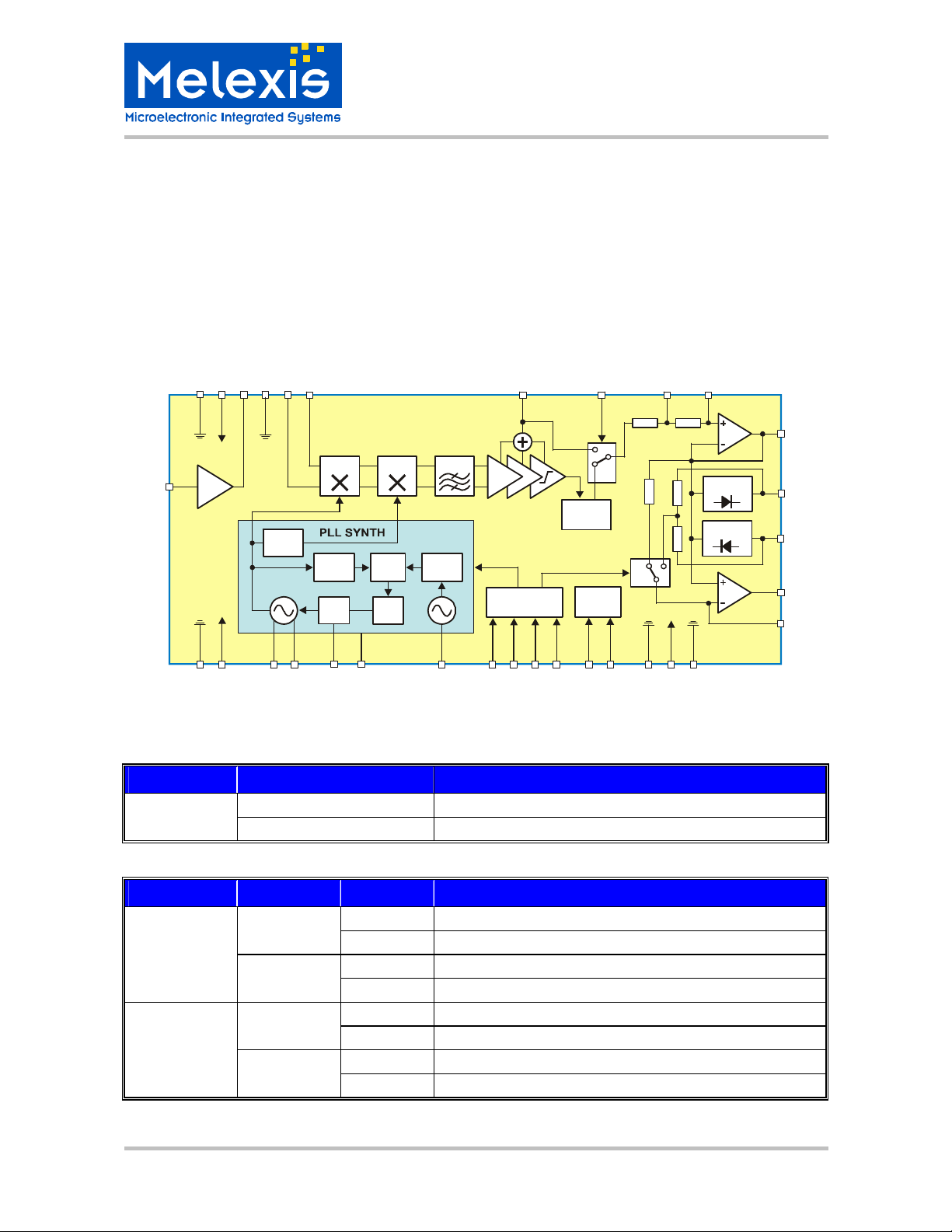
1 General Description
The PC programming software can be used to control the operational modes of the MLX71122 RF receiver at
its Serial Programming Interface (SPI) through the three pins A/SCLK, B/SDTA and C/SDEN. The pin
SPISEL must be at logic HIGH in order to set the MLX71122 to SPI mode. Otherwise the receiver operates in
stand-alone (or ABC) mode and cannot be programmed via the three pins A/SCLK, B/SDTA and C/SDEN.
In SPI mode, it is possible to write in and read out the seven control registers R0 to R6. Register R7 is a
read-only register for status information. In ABC mode, 8 predefined frequency channels between 369.5 MHz
and 395.9 MHz can be selected by parallel programming at the three pins A/SCLK, B/SDTA and C/SDEN.
A block diagram of the receiver is shown below.
2
1
VE
5
6
43
8
9
28
MODSEL
29
LO2
RO
R
counter
24
IFF
_
SLCSEL
Logic
30
ROI
17
SPISEL
2016 21
ENRX
RBIAS
LNAI
31
MIX1 MIX2
N / A
counter
LF
15
LO1
LF
IF1
PFD
CP
MFO
23
LNA
LO2DIV
VCO
TNK1 TNK2
VCCVCO
VEEVCO
1411
12 13
The following tables show the functionality of the three digital control pins that are used for general operating
mode selection.
E
Pin Value Function
SPISEL
0 ABC mode - stand-alone mode, 8 pre-defined frequencies
1 SPI mode - programmable mode, full control via SPI
Pin Value SPISEL Function
0
MODSEL
1
0
ENRX
1
0 FSK receive mode
1 no effect
0 ASK receive mode
1 no effect
0 Receiver in shutdown mode
1 Receiver in last programmed operational mode
0 Receiver in receive mode
1 Receiver in receive mode
39011 71122 01 Page 4 of 21 SW71122-Manual
Rev. 004 Aug/11
Page 5
P
R
L
I
M
I
N
A
R
Y
SW71122
MLX71122 RF Receiver
Programming Software Manual
2 Hardware and Software Requirements
The MLX71122 program has been developed for Windows XP and has been tested for later Windows versions. The program uses TVicPort I/O driver to interface to the parallel port.
The EVB71122 can be used either with a USB-SPI converter connected to the PC’s USB port or it can be
directly connected to the PC’s printer port (LPT). If the LPT port is used then port addresses 0x278, 0x378
and 0x3BC (hexadecimal) are supported. A programming cable with a male 25-pole SUB-D connector can be
purchased together with the evaluation board EVB71122.
The following LPT ports can be connected to the corresponding IC pins:
LPT port Direction IC pin Cable pin
BUSY (pin11) ←
GND (pin18-25)
D1 (pin3)
D2 (pin4) →
D0 (pin2) →
If the PC’s USB port is used, a USB-SPI converter is required. It is available on request or can be purchased
together with the evaluation board EVB71122.
Note that pin 7 of the MLX71122 (SPISEL) is connected to logic HIGH on the EVB71122. This is to set the
receiver to SPI mode.
→
MFO (pin 23) Connected (1)
GND
A/SCLK (pin 19) Connected (3)
B/SDTA (pin 18) Connected (4)
C/SDEN (pin17) Connected (5)
Connected (2)
3 Installation and Files
The installation program will ask you for a folder where you want to install the files. By default, the program
installs the software in the directory:
C:\Program Files\Melexis\MLX71122_V32
The following files will be installed:
File Function
MLX71122_V32.exe Main program executable
unins000.exe Program to uninstall the software
unins000.dat Uninstall data file
MLX71122.ini Init file for windows start of main program
TVicPort.dll Dynamic library to support parallel port programming
ReadMe.txt ReadMe file
mpusbapi.dll Dynamic library to support USB interface
\MLX_SPIUSB_Driver\mchpusb.cat USB driver
\MLX_SPIUSB_Driver\MLX-SPIUSB.inf USB driver
\MLX_SPIUSB_Driver\mchpusb.sys USB driver
\MLX_SPIUSB_Driver\mchpusb64.sys USB driver
Copyrights:
TVicPort I/O driver, © En Tech Taiwan
Windows XP, © Microsoft Corporation.
39011 71122 01 Page 5 of 21 SW71122-Manual
Rev. 004 Aug/11
E
Page 6
P
R
L
I
M
I
N
A
R
Y
SW71122
MLX71122 RF Receiver
Programming Software Manual
We recommend creating the icon of the main program on your PC’s desktop to easily access the program.
The working directory folder of the link should be set to the installation folder.
4 Using the Software
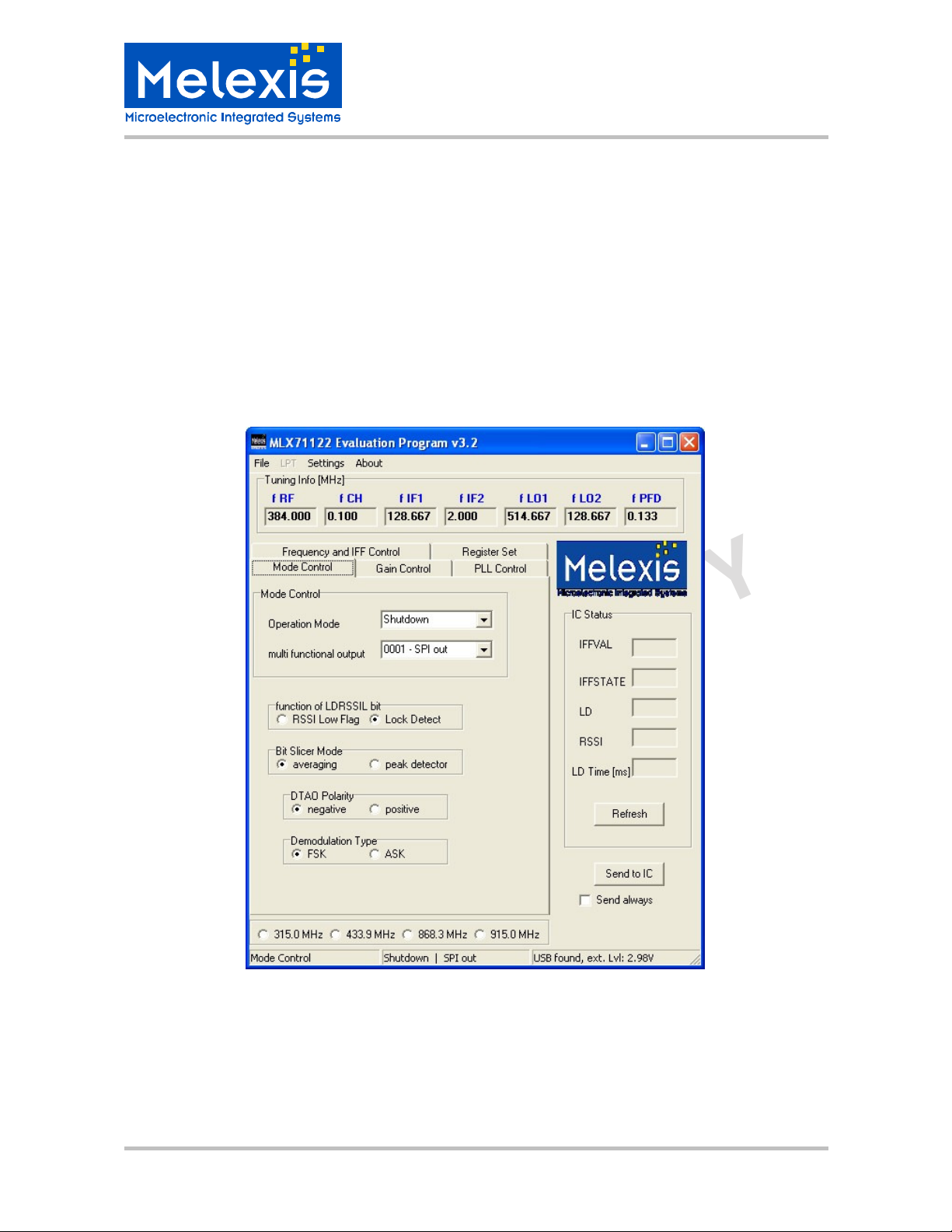
4.1 Software Start Up
Please make sure the evaluation board EVB71122 and the USB-SPI converter (or the LPT cable) are connected to the PC. This ensures that the software automatically detects whether the USB or the LPT port are
used.
The software can be started by double clicking on the main program icon in the installation directory or by
double clicking on the link. During start-up the software reads out the corresponding init-file and restores all
settings that were active when the software was regularly closed the last time.
E
A typical first menu view of the program is shown in the figure above. The program starts up with the tab
Mode Control activated.
Data is only sent to the IC if the Send to IC button is pressed or Send always is activated.
39011 71122 01 Page 6 of 21 SW71122-Manual
Rev. 004 Aug/11
Page 7

P
R
L
I
M
I
N
A
R
Y
SW71122
MLX71122 RF Receiver
Programming Software Manual
4.2 Menus
4.2.1 File
The menu File contains three menu items:
• Load Config load a previously defined config-file and activate the new state
• Save Config save the actual state in a new config-file
The Exit field in the window frame has the same function as the Exit menu item. After a configuration is
loaded its file name is displayed in the window title as reminder.
4.2.2 LPT
This menu enables the user to choose a LPT port address to use for the programming. Three port addresses
are supported (in hexadecimal):
The port address is displayed in the Program Status Line at the lower-right corner of the program window.
Note that if the USB-SPI converter is used the LPT menu cannot be selected (LPT appears gray shaded).
The Program Status Line shows that the USB-SPI converter has been found.
4.2.3 Settings
The menu Settings contains three menu items:
The Defaults menu item of this menu restores the state that is hard-coded on the MLX71122 and that is active after powering up the IC. The default receive frequency is 384MHz. After recovering the default settings
the text Default Settings is displayed in the window title as reminder.
The Set Vpwm menu item activates the internal reference voltage of the USB-SPI converter. It is freely programmable in a range of 0 to 5V. The voltage should be entered in millivolts.
If ext. Vref menu item is selected, the Set Vpwm menu item cannot be selected (appears gray shaded).
If the LPT port is used the ext. Vref and Set Vpwm menu items cannot be selected (appear gray shaded).
If the ext. Vref menu item is selected, but no external reference voltage is connected to the USB-SPI converter the SPI logical high level will be set internally to about 1.83V.
• Exit close the program and save the state into the init-file
• 0x278
• 0x378 (default)
• 0x3BC
• Defaults restores the state that is hard-coded on the MLX71122
• ext. Vref SPI logical high level set by external reference voltage (e.g. provided by supply
voltage of EVB71122)
• Set Vpwm SPI logical high level set by internal reference voltage
E
39011 71122 01 Page 7 of 21 SW71122-Manual
Rev. 004 Aug/11
Page 8

P
R
L
I
M
I
N
A
R
Y
4.2.4 About
SW71122
MLX71122 RF Receiver
Programming Software Manual
This menu displays a window with information about the LPT-port to pin connections.
E
This menu displays a window with information about the USB-SPI converter (only available if the USB-SPI
converter is used).
39011 71122 01 Page 8 of 21 SW71122-Manual
Rev. 004 Aug/11
Page 9

P
R
L
I
M
I
N
A
R
Y
4.3 Send to IC - Button
SW71122
MLX71122 RF Receiver
Programming Software Manual
After pressing the Send to IC button the registers R0 to R6 of the IC will be programmed with the data from
the actual state.
If the checkbox Send always is activated this operation is performed every time a control field is changed.
This can be used to simplify monitoring of single setting changes but it can produce unwanted intermediate
states if more than one setting has to be changed.
4.4 Tuning Info - Frame
The values of seven important frequencies are displayed in the tuning info frame:
• fRF: actual receive frequency
• fCH: channel step width
• f
: first intermediate frequency after the first mixer
IF1
• f
: second intermediate frequency after the second mixer
IF2
• f
• f
All frequencies are given in MHz with three post decimal positions.
• f
: VCO output frequency or LO input frequency of first mixer
LO1
: LO input frequency of second mixer (depends on f
LO2
: working frequency of the phase-frequency detector of the PLL
PFD
E
)
LO1
4.5 Program Status Line
The Status Line at the bottom of the program window displays three status values. The name of the actual
tab field is shown on the left hand side. The middle part displays the selected operation mode and the output
mode of the MFO pin separated by a vertical bar. On the right hand side is shown:
• the actual LPT port address if LPT port is used
• external reference voltage for SPI high logic level if USB-SPI converter is used and the ext. Vref
menu item is selected
• internal reference voltage for SPI high logic level if USB-SPI converter is used and Set Vpwm
menu item is selected.
39011 71122 01 Page 9 of 21 SW71122-Manual
Rev. 004 Aug/11
Page 10

P
R
L
I
M
I
N
A
R
Y
SW71122
MLX71122 RF Receiver
Programming Software Manual
4.6 IC Status - Frame
The IC Status frame displays information about the internal state of the IC if the Multi Functional Output
(MFO) mode is set to SPI out (left figure). A click on the Refresh button reads out the data from the MFO-pin
of the IC.
The following data is displayed:
Field Value Meaning
IFFVAL Integer number between 0 and 255 Tuning value of the internal IF filter
tuned Filter tuned or auto-tuning disabled
IFFSTATE
LD
RSSI
LD Time Time in ms Approximate PLL lock time
LD is only displayed if Lock Detect is selected in function of LDRSSIL bit or MFO-mode is set to
LD-out. In LD-out mode the additional field LD Time is displayed (right figure) and the PLL lock in time is
measured every time when data is send to the IC.
tune up Tuning up the filter frequency
tune dn Tuning down the filter frequency
CCO fail Master oscillator of filter does not work
locked PLL locked in
Not locked PLL not locked in
Low V
In range V
High V
E
in lower region
RSSI
in mid region
RSSI
in upper region
RSSI
4.7 Frequency Pre-Selection - Frame
Four fixed receive frequencies at 315.0MHz, 433.9MHz, 868.3MHz or 915.0MHz can be pre-selected to ease
the initialization of the receiver. All settings of the receiver are affected and are reset to their default value
with respect to the receive frequency.
39011 71122 01 Page 10 of 21 SW71122-Manual
Rev. 004 Aug/11
Page 11

P
R
L
I
M
I
N
A
R
Y
Programming Software Manual
5 Description of the Control Tabs
The user can select five tabs for different control settings of the SPI-mode.
5.1 Mode Control – Tab
SW71122
MLX71122 RF Receiver
The Mode Control tab displays all dialog fields that are used to change the operating modes of the circuit. On
top are the controls for the Operation Mode and the mode of the Multi Functional Output (MFO).
5.1.1 Operation Mode
Selections are:
• Shutdown all blocks deactivated, only SPI active (default)
• Receive receiving data from LNAI at selected frequency
• RO and bias only only biasing system and reference oscillator are working
The first operation mode consumes virtually no current. The circuit is dead except of the SPI that can listen to
commands. In Receive mode all necessary blocks are turned on to receive data at the programmed
frequency.
The last two operation modes can be used to accelerate the start-up of the circuit after periods of silence.
With RO and biasing only, the long start-up time of the reference oscillator (RO) can be circumvented. RO
and biasing consume not as much current as the whole receiver. With Synthesizer only the full PLL is
already working and locked in. Current consuming blocks as the LNA, the IF-filter and the FSK-demodulator
are turned off in this state. The last mode is useful if the receiver has to listen in short periods.
39011 71122 01 Page 11 of 21 SW71122-Manual
Rev. 004 Aug/11
• Synthesizer only only biasing system, reference oscillator and PLL are working
E
Page 12

P
R
L
I
M
I
N
A
R
Y
SW71122
MLX71122 RF Receiver
Programming Software Manual
5.1.2 Multi Functional Output Mode
Selections are:
• Z-State MFO pin is in high impedance mode
• SPI-out MFO pin is digital serial output for data of register R7 (default)
• Logic-0 MFO pin is pulled to ground
• Logic-1 MFO pin is pulled to VCC
• RO-out MFO pin is buffered, analogue output of RO frequency
• IF-out MFO pin is buffered, analogue output of IF2 signal after the IF-filter
All other visible selections are only for test purposes and have no significant value if the circuit is operating on
the evaluation board.
Z-State, Logic-0 and Logic-1 can be used to control an additional digital input on the board if no microcontroller output is available. With RO-out a 10MHz clock frequency is available on the board that can also be used
to save one quartz crystal by driving the RO of another MLX71122 receiver. IF-out provides the internal IF2
signal amplified by a factor of 5 if the MFO-pin is unloaded. The output resistance is about 610Ω in this mode.
The IF-out mode can be used to further filter the IF2 signal. In this case an external limiting amplifier and
demodulator must be used.
With LD-out the state of the PLL can be detected. The lock state is also displayed in the LD field of the IC
Status frame. An additional field in the IC Status frame appears that can display the approximate lock in
time in ms measured by the PC. This is not very accurate!
In SPI-out mode the data of register R7 can be read out and the different circuit states are displayed in the IC
Status frame.
• LD-out MFO pin represents lock state of PLL
5.1.3 Function of LDRSSIL bit
Unfortunately there is more information available than bits in R7. So, these radio buttons select the output
that is multiplexed to bit 11 of register R7. One can either select the output of the RSSI low flag or the Lock
Detection flag (default) of the PLL. The selection affects the output displayed in the IC Status frame.
5.1.4 Bit Slicer Mode
These radio buttons control which data slice mode is used. One can either select averaging mode (default)
that uses a RC-low pass to generate the reference voltage or peak detector mode that uses the median as
reference for the output comparator.
5.1.5 DTAO Polarity
At positive polarity (default) the DTAO output is high if the DFO voltage is higher than the reference voltage
and vice versa.
5.1.6 Demodulation Type
This selects the type of demodulator to use. In case of ASK demodulation the FSK demodulator is turned off
and the RSSI pin is internally connected to the data filter. In FSK mode (default) the FSK demodulator output
is connected to the data filter but the RSSI voltage is still available at the RSSI pin.
E
39011 71122 01 Page 12 of 21 SW71122-Manual
Rev. 004 Aug/11
Page 13

P
R
L
I
M
I
N
A
R
Y
5.2 Gain Control – Tab
SW71122
MLX71122 RF Receiver
Programming Software Manual
The Gain Control tab is split up into an upper part defining the static gain of different receiver blocks and a
lower part for controlling the Automatic Gain Control (AGC).
The frame Receiver Gain Settings contains the following controls:
5.2.1 LNA
Four different LNA gain settings are possible. Since the absolute gain depends on the input matching of the
LNA and on the quality factor of the tank circuit, only settings relative to the default gain are selectable. The
gain is controlled by the core current of the LNA.
Possible selections are: Default -20dB, Default -6dB, Default -2dB, Default
5.2.2 IF Filter
The Intermediate Frequency Filter (IFF) has four gain settings: -14dB, -6dB, 0dB (default), +6dB.
These are absolute voltage gains from the filter input to the input of the Intermediate Frequency Amplifier
(IFA). Default gain is +6dB. If MFO is set to IF-out, 14dB have to be added for the gain from the filter input to
the unloaded MFO-pin and -9dB have to be added for the gain from the filter input to the MFO-pin with 50Ω
load. The output resistance of the MFO-buffer is about 610Ω.
5.2.3 1st Mixer Gain
These radio buttons set the MIX1GAIN bit. It specifies the gain of the 1st mixer.
Possible selections are: 0dB, +14dB (default)
E
39011 71122 01 Page 13 of 21 SW71122-Manual
Rev. 004 Aug/11
Page 14

P
R
L
I
M
I
N
A
R
Y
SW71122
MLX71122 RF Receiver
Programming Software Manual
5.2.4 2nd Mixer Gain
These radio buttons set the MIX2GAIN bit. It specifies the gain of the 2nd mixer.
Possible selections are: -2dB, +9dB (default)
5.2.5 Demodulator Gain
These radio buttons control the frequency to voltage conversion gain of the FSK-demodulator:
• low 12mV/kHz (default)
The Automatic Gain Control (AGC) enables the circuit to keep its internal voltage amplitude levels in the
linear operation range of the different front end blocks. By default the gain settings are high to keep the noise
contribution of the active IF-filter as low as possible. If the input signal increases the filter will soon become
nonlinear because the input level is too high. A digital control circuit of the MLX71122 can be used to lower
the gains of the previous blocks to maintain the linear input range of the IF-filter as far as possible. First the
gain of mixer 2 is lowered, then mixer 1 and in the end the LNA gain.
5.2.6 RSSI Gain
The RSSIGAIN setting determines the RSSI gain of the IFA:
The output voltage range of the RSSI voltage will also be affected by this setting.
• high 14.5mV/kHz
• low 39mV/dB
• high 51mV/dB (default)
5.2.7 Enable AGC
This checkbox enables or disables (default) the AGC feature. Make sure that RSSIGAIN is high to use AGC.
5.2.8 Delay Settings
The AGC circuit uses the RSSIL and RSSIH flags to specify whether the gains have to be increased or
decreased. In order to make the gain switching independent of short signal fluctuations, four delay times are
selectable that specify how long the RSSIL or RSSIH flags have to be set before the gains are changed. The
delays are related to the reference frequency of the IF-filter adjustment circuit f
frequency is 10MHz then f
• Selectable delays are 0 / f
• or for 10 MHz RO frequency 0µs (default), 1µs, 5µs, 10.3µs
5.2.9 Delay Mode
These radio buttons specify whether the delay is only applied at gain increase and not at decrease (default),
or for both, increase and decrease.
should be equal to 3MHz.
IFF
E
(default), 3 / f
IFF
IFF
, 15 / f
. If the reference oscillator
IFF
IFF
, 31 / f
IFF
39011 71122 01 Page 14 of 21 SW71122-Manual
Rev. 004 Aug/11
Page 15

P
R
L
I
M
I
N
A
R
Y
5.3 PLL Control – Tab
SW71122
MLX71122 RF Receiver
Programming Software Manual
The PLL Control tab contains settings for the PLL and the VCO.
5.3.1 LDTIME
This selection box specifies the minimum time delay before a lock in of the PLL occurs after start of the PLL.
It is related to the reference frequency fR of the PFD.
Four possible time delays are selectable: 2 / fR, 4 / fR, 8 / fR, 16 / fR (default)
5.3.2 LDERR
These radio buttons specify how long the up and down pulses of the PFD can be different without loosing the
lock in state. If the PLL is locked in, these times of different up and down signals should be very small since
there is no correction of the VCO frequency necessary. If not, the power of the reference spurs in the VCO
output signal will increase. This can be the case for leaky capacitors in the loop filter. If the default for LDERR
of 15ns is not sufficient to keep the lock in state, it can be increased to 30ns.
5.3.3 CPCUR
This selection box specifies the charge pump current which is important to know for the design of the PLL
loop-filter. The charge pump is controlled by a Phase-Frequency-Detector (PFD) that makes it possible to
control phase as well as frequency deviations of the VCO. Four different settings are selectable:
• 100µA ±100µA (default)
• 400µA ±400µA
• 400µA Dn drains 400µA from pin LF to ground; static down
• 400µA Up sources 400µA from VCC to pin LF; static up
E
39011 71122 01 Page 15 of 21 SW71122-Manual
Rev. 004 Aug/11
Page 16

P
R
L
I
M
I
N
A
R
Y
SW71122
MLX71122 RF Receiver
Programming Software Manual
5.3.4 ROCUR
This selection box sets the core current of the reference oscillator. It should not be changed unless there is a
reason to do it.
Four current selections are available: 85µA, 170µA, 270µA, 355µA (default)
5.3.5 PRESCUR
The PRESCUR radio buttons specify the bias current of the PLL prescaler. The prescaler is a block that
works at the highest operating frequency of the circuit since it divides the VCO output signal. At high VCO
frequencies and under certain ambient conditions it may be necessary to increase its bias current from the
20µA (default) to 30µA to keep it dividing correctly.
5.3.6 PFDPOL
The polarity of the PDF should not be changed if the standard test circuit is used where only a tank inductor is
placed between pins TNK1 and TNK2. Default value is negative. If the loop filter voltage to frequency characteristic changes the sign of its slope, then it is necessary to change the PDF polarity. This can be the case if
an external VCO is used or if an additional element with controllable reactance is connected between the pins
TNK1 and TNK2.
5.3.7 VCO Range
The MLX71122 is designed for V
used down to 3V if this value is set to 3V. The most critical part at lower supply voltages is the VCO range
which can be adjusted with this setting. For supply voltages in between, the optimal setting must be found by
experiment.
5.3.8 VCO Buffer Current
The output buffer of the VCO works at the highest operating frequency of the circuit. Since it has to drive the
prescaler with a digital signal, the core current of the buffer can be increased from about 900µA (default) to
1040µA if it is necessary at high VCO frequencies and under certain ambient conditions.
5.3.9 VCO Core Current
The VCO core works at the highest operating frequency of the circuit. Its core current can be increased from
about 450µA (default) to 520µA if it is necessary at high VCO frequencies and under certain ambient
conditions.
= 5V so the default value of this setting is 5V. Nevertheless, it can be
CC
E
39011 71122 01 Page 16 of 21 SW71122-Manual
Rev. 004 Aug/11
Page 17

P
R
L
I
M
I
N
A
R
Y
5.4 Frequency and IFF Control – Tab
SW71122
MLX71122 RF Receiver
Programming Software Manual
The Frequency and IFF Control tab contains settings for the IF-filter auto-adjustment circuit and for the
control of the receive frequency.
The IF-Filter Auto-Adjustment Control uses a digitally controlled oscillator that works like a digital PLL. Its
reference frequency, which is by default at about 3MHz, is derived from the RO frequency by dividing fRO by
RIFF Divider and multiplying it by 200. The digital control word of the filter oscillator also controls the centre
frequency of the filter (2MHz). This is possible because it uses the same transconductance cells as the oscillator. The tab offers several fields to control the adjustment circuit.
5.4.1 Auto Adjustment
This checkbox controls whether the auto-adjustment is turned on or off. If it is turned on (default), it corrects
continuously the centre frequency of the filter. If it is turned off, then the actual IFF Preset Value is loaded
into the digital control word and the auto-tuning stops with this value. The filter works with this IFF Preset
Value if auto-adjustment is deactivated and the IFFSTATE (see section 4.6) changes to tuned. After enabling
the auto-tuning again the process starts with the previously loaded IFF Preset Value.
5.4.2 Halt
This checkbox interrupts the auto-tuning process but leaves the last control value in the internal register. After
deactivating this box the tuning process continues with this value.
5.4.3 RIFF Divider
This value controls the ratio of the IF filter oscillator frequency to the RO frequency. Default value is 684.
E
39011 71122 01 Page 17 of 21 SW71122-Manual
Rev. 004 Aug/11
Page 18

P
R
L
I
M
I
N
A
R
Y
SW71122
MLX71122 RF Receiver
Programming Software Manual
5.4.4 IFF Preset Value
This value is the start value of the digitally controlled filter oscillator. It is loaded into the internal control word
register after start-up or if the auto-tuning is deactivated. Default value is 91.
5.4.5 IFF centre freq.
This field displays the actual centre frequency of the filter with respect to all settings. It should be 2MHz
because it is the IF2. Also slightly different IF-frequencies are possible in order to correct frequency deviations caused by an inappropriate channel step width.
5.4.6 f
This is the oscillator frequency of the quartz crystal oscillator. The IC is designed for a f
5.4.7 R Divider
This is the reference divider value by that the RO frequency is divided to provide the reference frequency for
the PFD. Default value is 75.
5.4.8 fRF
It is possible to enter the desired receive frequency in this field. The N and A counter values are calculated
from this entry when the calculate button is pressed. Default receive frequency is 384MHz.
5.4.9 A
This is the A counter of the pulse swallow feedback divider of the PLL. The total feedback divider value is
calculated with N
5.4.10 N
This is the N counter of the pulse swallow feedback divider of the PLL. The total feedback divider value is
calculated with N
XTAL
= 32·N+A. Default value is 20.
TOT
E
= 32·N+A. Default value is 120.
TOT
of 10MHz!
XTAL
5.4.11 N
This is the total feedback divider value which is calculated with N
can not be changed.
5.4.12 Calculate Button
The Calculate button triggers the calculation of new N and A counter values from the entered fRF with
respect to all other settings.
39011 71122 01 Page 18 of 21 SW71122-Manual
Rev. 004 Aug/11
TOT
=32·N+A. Default value is 3860. This field
TOT
Page 19

P
R
L
I
M
I
N
A
R
Y
SW71122
MLX71122 RF Receiver
Programming Software Manual
5.4.13 LO1
The frame Injection Side defines the injection side of the LO signals into the mixers. At high side injection
the LO signal has a higher frequency than the other input signal of the mixer and vice versa. The LO1 value
is only used for calculation reasons since it has no effect on the register settings. On the other hand it has
much impact on the required LO1 frequency. Default value is high. The effect of the LO1 setting can be
observed in the Tuning Info frame (see figure in section 4.4).
5.4.14 LO2
Since mixer 2 is an image rejection mixer, we can select the right mixing product by selecting the right injection side for LO2. Default value is high. The effect of the LO2 setting can be observed in the Tuning Info
frame (see figure in section 4.4).
5.4.15 LO2DIV
These radio buttons specify the divider ratio by that the LO2 frequency is lower than the LO1 frequency. LO1
is injected into mixer 1 and LO2 is injected into mixer 2.
5.5 Register Set - Tab
E
The Register Set tab gives an overview of all actual control word registers of the IC (see Data Sheet
section 4). Registers R0 to R7 with all their bits are displayed from top to bottom. The most significant bits are
on the left hand side. Red fields mean the bit is high, blue fields mean the bit is low. For ease of use the corresponding word value in hexadecimal notation is shown on the right hand side of each control word.
Single bits can be manipulated in this tab. If the mouse pointer is moved over a field, then the bit name will be
displayed in the status field at the bottom of the dialog window and directly at the location of the mouse
pointer. A single click on a bit field toggles the state of this bit between low and high.
39011 71122 01 Page 19 of 21 SW71122-Manual
Rev. 004 Aug/11
Page 20

P
R
L
I
M
I
N
A
R
Y
Your Notes
SW71122
MLX71122 RF Receiver
Programming Software Manual
E
39011 71122 01 Page 20 of 21 SW71122-Manual
Rev. 004 Aug/11
Page 21

P
R
L
I
M
I
N
A
R
Y
SW71122
MLX71122 RF Receiver
Programming Software Manual
For the latest version of this document, go to our website at:
Or for additional information contact Melexis Direct:
Europe and Japan: All other locations:
Phone: +32 1367 0495 Phone: +1 603 223 2362
E-mail: sales_europe@melexis.com E-mail: sales_usa@melexis.com
E
www.melexis.com
ISO/TS16949 and ISO14001 Certified
39011 71122 01 Page 21 of 21 SW71122-Manual
Rev. 004 Aug/11
 Loading...