

Page 1

Analog-Digital Converter Module type AJ65SBT-64AD
User,s Manual
Mitsubishi Programmable Logic Controller
Page 2
SAFETY PRECAUTIONS
(Always read these precautions before using this equipment.)
Before using this product, please read this manual and the relevant manuals introduced in this manual
carefully and pay full attention to safety to handle the product correctly.
The precautions given in this manual are concerned with this product. Refer to the user’s manual of the
CPU module to use for a description of the PLC system safety precautions.
In this manual, the safety instructions are ranked as "DANGER" and "CAUTION".
DANGER
!
CAUTION
!
Note that the !CAUTION level may lead to a serious consequence according to t he circumstances.
Always follow the precautions of both levels because they are important t o personal safety.
Please save this manual to make it accessible when required and always forw ard it to the end user.
Indicates that incorrect handling may cause hazardous conditions,
resulting in death or severe injury.
Indicates that incorrect handling may cause hazardous conditions,
resulting in medium or slight personal injury or physical damage.
[Design Precautions]
!
DANGER
When there are communication problems with the data link, the data for the master module will
be held.
Configure an interlocking circuit in a sequence program so that the safety of the overall sy stem
is always maintained.
!
CAUTION
Do not bunch the control wires or communication cables with the main circuit or power wires, or
install them close to each other.
They should be installed 100mm (3.9inch) or more from each other.
Not doing so could result in noise that would cause erroneous operation.
A - 1
Page 3

[Installation Precautions]
!
CAUTION
Use the PLC in the environment that meets the general specifications contain ed in this Manual.
Using the PLC outside the range of the general specifications may result in electr ic shock, fire or
malfunction, or may damage or degrade the module.
Securely fix the module to a DIN rail or with mounting screws, and securely tighten the mounting
screws within the specified torque range.
Undertightening can cause a drop or malfunction.
Overtightening can cause a drop or malfunction due to damage of the screws or module.
Do not touch the conducted area or electric parts of the module.
Doing so may cause module malfunctioning or breakdowns.
[Wiring Precautions]
!
CAUTION
Always switch power off externally in all phases before starting installation, w iring and other
works.
Not doing so can cause the product to be damaged or malfunction.
Always earth the FG and FG1 terminals to the protective earth conductor.
Not doing so can cause a malfunction.
Wire the module correctly after confirming the rated voltage and terminal layout of the product.
Not doing so can cause a fire or failure.
Tighten the terminal screws within the specified torque range.
Undertightening can cause a short circuit or malfunction.
Overtightening can cause a short circuit or malfunction due to damage of the screws or module.
Ensure that no foreign matter such as chips and wire-offcuts enter the module.
Foreign matter can cause a fire, failure or malfunction.
A - 2
Page 4
[Wiring Precautions]
!
CAUTION
When connecting the communication and power supply cables to the module, alway s run them
in conduits or clamp them.
Not doing so can damage the module and cables due to loose, moved or accidentally pulled
cables or can cause a malfunction due to a cable connection fault.
When disconnecting the communication and power supply cables from the module, do not hold
and pull the cable part.
Disconnect the cables after loosening the screws in the portions connected t o the module.
Pulling the cables connected to the module can damage the module and cables or can cause a
malfunction due to a cable connection fault.
[Starting and Maintenance Precautions]
!
CAUTION
Do not touch the terminals while the power is on. Doing so may cause malfunctioning.
Always start cleaning or terminal screw retightening after switching power off externally in all
phases.
Not doing so can cause the module to fail or malfunction.
Undertightening can cause a drop, short circuit or malfunction.
Overtightening can cause a drop, short circuit or malfunction due to damage of the screws or
module.
Never disassemble or modify the module.
This may cause breakdowns, malfunctioning, injury and/or fire.
Do not drop the module or give it hard impact since its case is made of resin. Doing so can
damage the module.
Mount or dismount the module to or from an enclosure after switching power off externally in all
phases.
Not doing so can cause the module to fail or malfunction.
[Disposal Precautions]
!
CAUTION
When disposing of this product, treat it as industrial waste.
A - 3
Page 5

REVISIONS
* The manual number is given on the bottom left of the back cov er.
Print Date * Manual Number Revision
Oct., 2000 SH (NA) 080106-A First printing
Japanese Manual Version SH-080087-A
This manual confers no industrial property rights or any rights of any other kind, nor doe s it confer any patent licenses.
Mitsubishi Electric Corporation cannot be held responsible for any problems inv olv ing industria l property rights which
may occur as a result of using the contents noted in this manual.
2000 MITSUBISHI ELECTRIC CORPORATION
A - 4
Page 6

INTRODUCTION
Thank you for choosing a Mitsubishi MELSEC-A Series General Purpose Programmable Controller.
Before using your new PLC, please read this manual thoroughly to gain an understanding of its functions so
you can use it properly.
CONTENTS
SAFETY PRECAUTIONS..............................................................................................................................A- 1
REVISIONS....................................................................................................................................................A- 4
About Manuals ...............................................................................................................................................A- 7
Conformation to the EMC Directive and Low Voltage Instruction ................................................................A- 7
About the Generic Terms and Abbreviations ................................................................................................A- 8
Product components......................................................................................................................................A- 9
1. OVERVIEW 1- 1 to 1- 2
1.1 Features ...................................................................................................................................................1- 1
2. SYSTEM CONFIGURATION 2- 1 to 2- 2
2.1 Overall Configuration ...............................................................................................................................2- 1
2.2 Applicable System....................................................................................................................................2- 2
3 SPECIFICATION 3- 1 to 3- 16
3.1 General Specification...............................................................................................................................3- 1
3.2 Performance Specification.......................................................................................................................3- 2
3.3 I/O Conversion Characteristics................................................................................................................3- 3
3.3.1 Voltage input characteristics.............................................................................................................3- 4
3.3.2 Current input characteristics ............................................................................................................. 3- 5
3.3.3 Relationship between the offset/gain setting and digital output value............................................. 3- 6
3.3.4 Accuracy............................................................................................................................................3- 6
3.3.5 Conversion speed .............................................................................................................................3- 7
3.4 Function List .............................................................................................................................................3- 8
3.4.1 Sampling processing.........................................................................................................................3- 9
3.4.2 Moving average processing..............................................................................................................3- 9
3.5 Remote I/O Signals.................................................................................................................................3- 10
3.5.1 Remote I/O signal list.......................................................................................................................3- 10
3.5.2 Functions of the remote I/O signals.................................................................................................3- 11
3.6 Remote Register.....................................................................................................................................3- 13
3.6.1 Remote register allocation...............................................................................................................3- 13
3.6.2 A/D conversion enable/prohibit specification (Address RWwm)....................................................3- 14
3.6.3 Input range setting (Address RWwm+1).........................................................................................3- 15
3.6.4 Moving average processing count setting (Address RWwm+2) ....................................................3- 16
3.6.5 CH.
Digital output value (Address RWrn to RWrn+3).................................................................3- 16
A - 5
Page 7

4 SETUP AND PREPARATION BEFORE OPERATION 4- 1 to 4- 10
4.1 Pre-Operation Procedure.........................................................................................................................4- 1
4.2 Precautions When Handling....................................................................................................................4- 1
4.3 Name of Each Part...................................................................................................................................4- 3
4.4 Offset/Gain Setting...................................................................................................................................4- 5
4.5 Station Number Setting............................................................................................................................4- 7
4.6 Facing Direction of the Module Installation .............................................................................................4- 7
4.7 Data Link Cable Wiring ............................................................................................................................4- 8
4.7.1 Instructions for handling the CC-Link dedicated cables...................................................................4- 8
4.7.2 Connection of the CC-Link dedicated cables...................................................................................4- 8
4.8 Wiring........................................................................................................................................................4- 8
4.8.1 Wiring precautions.............................................................................................................................4- 8
4.8.2 Module connection example.............................................................................................................4- 9
4.9 Maintenance and Inspection....................................................................................................................4- 9
5 PROGRAMMING 5- 1 to 5- 18
5.1 Programming Procedure..........................................................................................................................5- 1
5.2 Program Examples .................................................................................................................................. 5- 2
5.2.1 Program examples for use of the ACPU/QCPU (A mode) (FROM/TO instructions)...................... 5- 2
5.2.2 Program examples for use of the ACPU/QCPU (A mode) (dedicated instructions).......................5- 7
5.2.3 Program examples for use of the QnACPU....................................................................................5- 12
5.2.4 Program examples for use of the QCPU (Q mode)........................................................................5- 15
6 TROUBLESHOOTING 6- 1 to 6- 6
6.1 Using the Remote Input Signals to Check Errors...................................................................................6- 1
6.2 Using the LED Indications to Check Errors............................................................................................. 6- 2
6.3 When the digital output value cannot be read.........................................................................................6- 4
6.4 Troubleshooting for the Case where the "ERR." LED of the Master Station Flickers ...........................6- 5
APPENDIX Appendix- 1 to Appendix- 4
Appendix1 Comparison between This Product and Conventional Product....................................Appendix- 1
Appendix2 External dimension diagram...........................................................................................Appendix- 3
A - 6
Page 8

About Manuals
Related Manu al s
The following manuals are also related to this product.
In necessary, order them by quoting the details in the tables below.
Manual Name
CC-Link System Master/Local Module User's Manual ty pe AJ61BT11/A1SJ61BT 11
Describes the system configuration, performance specifications, functions, handling, wiring and
troubleshooting of the AJ61BT11 and A1SJ61BT11. (Optionally available)
CC-Link System Master/Local Module User's M anual type AJ61Q BT 11/A1SJ61QBT11
Describes the system configuration, performance specifications, functions, handling, wiring and
troubleshooting of the AJ61QBT11 and A1SJ61QBT11. (Optionally available)
CC-Link System Master/Local Module User's Manual ty pe QJ61BT 11
Describes the system configuration, performance specifications, functions, handling, wiring and
troubleshooting of the QJ61BT11. (Optionally available)
Programming Manual type AnSHCPU/AnACPU/AnUCPU/QCPU-A (A Mode) (Dedicated
Instructions)
Explains the instructions extended for the AnSHCPU/AnACPU/AnUCPU/QCPU-A (A Mode).
(Optionally available)
Manual Number
(Model Code)
IB-66721
(13J872)
IB-66722
(13J873)
SH-080016
(13JL91)
IB-66251
(13J742)
Conformation to the EMC Directive and Low Voltage Instruction
When complying with EMC Directives and Low-Voltage Directives by assembling a
Mitsubishi PLC compa t ibl e wi th EM C Di re ctiv e an d Low -V olta ge Di r e ctive s in to th e
user product, refer to Chapter 3 "EMC Directives and Low-Voltage Directives" in the
User’s Manual (Hardware) for the CPU module being used.
The CE logo is printed on the rating plate on the main body of the PLC that conforms
to the EMC directive and low voltage instruction.
A - 7
Page 9

About the Generic Terms and Abbreviations
Unless otherwise specified, the following generic terms and abbreviations are used in
this manual to describe Type AJ65SBT-64AD analog-digital converter module.
Generic Term/Abbreviation Description
GPPW Abbreviation for the SW4D5C-GPPW-E or later GPP function software.
Generic term for A0J2CPU, A0J2HCPU, A2CPU, A2CPU-S1, A3CPU, A1SCPU,
A1SCPU-S1, A1SCPUC-24-R2, A1SHCPU, A1SJCPU, A1SJCPU-S3, A1SJHCPU,
ACPU
QnACPU
QCPU (A mode) Generic term for Q02CPU-A, Q02HCPU-A, Q06HCPU-A
QCPU (Q mode) Generic term for Q02CPU, Q02HCPU, Q06HCPU, Q12HCPU, Q25HCPU
Master station
Local station
Remote I/O station
Remote device station
Remote station
Intelligent device station
Master module
SB
SW
RX
RY
RWw
RWr
A1NCPU, A2NCPU, A2NCPU-S1, A3NCPU, A3MCPU, A3HCPU, A2SCPU, A2SCPUS1, A2SHCPU, A2SHCPU-S1, A2ACPU, A2ACPU-S1, A3ACPU, A2UCPU, A2UCPUS1, A2ASCPU, A2ASCPU-S1, A2ASCPU-S30, A2USHCPU-S1, A3UCPU, A4UCPU
Generic term for Q2ACPU, Q2ACPU-S1, Q2ASCPU, Q2ASCPU-S1, Q2ASHCPU,
Q2ASHCPU-S1, Q3ACPU, Q4ACPU, Q4ARCPU
Station that controls the data link system.
One master station is required for each system.
Station having a PLC CPU and the ability to communicate with the master and other
local stations.
Remote station that handles bit unit data only. (Performs input and output with external
devices.) (AJ65BTB1-16D, AJ65SBTB1-16D)
Remote station that handles bit unit and word unit data only. (Performs input and output
with external devices, and analog data exchange.)
Generic term for remote I/O station and remote device station.
(Controlled by the master station)
Station that can perform transient transmission, such as the AJ65BT -R 2 (including lo cal
stations).
Generic term for QJ61BT11, AJ61BT11, A1SJ61BT11, AJ61QBT11, and
A1SJ61QBT11 when they are used as master stations.
Link special relay (for CC-Link)
Bit unit information that indicates the module operating status and data lin k status of the
master station/local station. (Expressed as SB for convenience)
Link special register (for CC-Link)
16 bit unit information that indicates the module operating status and data l ink st atus of
the master station/local station. (Expressed as SW for convenience)
Remote input (for CC-Link)
Information entered in bit units from the remote station to the master statio n. (Expressed
as RX for convenience)
Remote output (for CC-Link)
Information output in bit units from the master station to the remote station. (Expressed
as RY for convenience)
Remote register (Write area for CC-Link)
Information output in 16-bit units from the master station to the remote dev ice st ation.
(Expressed as RWw for convenience)
Remote register (Read area for CC-Link)
Information entered in 16-bit units from the remote device station to the master stat ion.
(Expressed as RWr for convenience)
A - 8
Page 10

Product components
This product consists of the following.
Product Name Quantity
Type AJ65SBT-6 4AD an alo g- dig it al conv e rte r module
Type AJ65SBT-64AD analog-digital converter module user's manual (hardware)
1
1
A - 9
Page 11

MEMO
A - 10
Page 12

1 OVERVIEW
1 OVERVIEW
1.1 Features
MELSEC-A
1
This user's manual explains the specifications, handling, programming methods and
others of Type AJ65SBT-64AD analog-digital converter module (hereafter abbreviated
to the "AJ65SBT-64AD") which is used as a remote device station of a Control &
Communication Link (hereafter abbreviated to "CC-Link") system.
The AJ65SBT-64AD conv e rt s the anal og sig nal s (vol ta g e o r cur ren t inpu t ) fr om th e
PLC's external source to a 16-bit encoded binary data digital value.
This section gives the features of the AJ65SBT-64AD.
(1) High accuracy
This module performs A/D conversion at the accuracy of ±0.4% relative to the
maximum value of the digital output value at the operating ambient temperature
of 0 to 55°C, o r at ± 0 .2 % rel a tive to the maximum v a lu e o f the di gi ta l ou t pu t val ue
at the operating ambient temperature of 25±5°C.
(2) Input range selectable per channel
You can choose the analog input range per channel to change the I/O conversion
characteristics.
(3) High resolution of 1/±4000
By changing the input range, you can choose and set the digital value resolution
to either 1/4000 or 1/±4000 (when the -10 to +10V range or user range setting 1
is selected) to p rov id e hi gh -re so lution digital value s.
(4) Designation of sampling processing or movi ng av erage pr ocessing
As a conversion method, you can specify sampling processing or moving
average processing per channel.
(5) Smaller than the conventional A/D converter module
This module is 60% smaller in installation area and 38% less in volume than the
conventional CC -Lin k A/ D co nve rt e r modul e (A J65B T-6 4A D) .
(6) Up to 42 modules connectable
You can connect up to 42 AJ65SBT-64AD modules to one master station.
1 - 1
Page 13

1 OVERVIEW
MEMO
MELSEC-A
1 - 2
Page 14

2 SYSTEM CONFIGURATION
2 SYSTEM CONFIGURATION
This chapter describes the system configuration for use of the AJ65SBT-64AD.
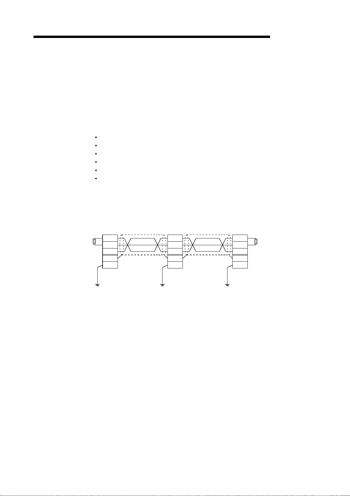
2.1 Overall Configuration
The overall configuration for use of the AJ65SBT-64AD is shown below.
MELSEC-A
2
CC-Link master/local module (master station)
(AJ61BT11, A1SJ61BT11, AJ61QBT11,
A1SJ61QBT11, QJ61BT11)
Terminal resistor
(Intelligent device st a t io n) (Remote I/O station)
Terminal resistor
AJ65SBT-64AD
(Remote device station)
CC-Link master/local module (local station)
(AJ61BT11, A1SJ61BT11, AJ61QBT11, A1SJ61QBT11, QJ61BT11)
CC-Link dedicated cable
(Remote device station)
1 station occupied
RX/RY: 32 points each
RWr/RWw: 4 points each
Object whose
voltage/current
will be detected
2 - 1
Page 15

2 SYSTEM CONFIGURATION
2.2 Applicable System
This section explains the applicable system.
(1) Applicable master modules
The following master modules can be used with the AJ65SBT-64AD.
AJ61BT11
A1SJ61BT11
AJ61QBT11
A1SJ61QBT11
QJ61BT11
(2) Restrictions on use of CC-Link dedicated instructi ons
The CC-Link dedicated instructions may not be used depending on the PLC CPU
or master module used.
For details of the restrictions, refer to the A series master module user's manual.
MELSEC-A
2 - 2
Page 16
3 SPECIFICATION
3 SPECIFICATION
This chapter provides the specifications of the AJ65SBT-64AD.
3.1 General Specification
Table 3.1 indicates the general specifications of the AJ65SBT-64AD.
MELSEC-A
Table 3.1 General specification
Item Specification
Usage ambient temperature 0 to 55°C
Storage ambient temperature -20 to 75°C
Usage ambient humidity 10 to 90%RH, no condensation
Storage ambient humidity 10 to 90%RH, no condensation
When there is intermittent vibration
Frequency Acceleration Amplitude Sweep count
10 to 57Hz —
2
Vibration durability
Shock durability
Usage environment No corrosive gas
Usage height Less than 2000 m (less than 6562 ft.)
Installation area Within the control board
Over-voltage category *
Pollution level *
1
2
*1 Indicates the location where the device is connected from the public cable network to the device structure wiring
area.
Category II applies to the devices to which the power is supplied from a fixed equipment.
Surge withstand voltage for devices with up to 300V of rated voltage is 2500V.
Conforming to JIS B
3501, IEC 1131-2
Conforming to JIS B 3501, IEC1131-2 (147m/s
57 to 150Hz
When there is continuous vibration
Frequency Acceleration Amplitude
10 to 57Hz —
57 to 150Hz
9.8m/s
2
4.9m/s
Less than II
Less than 2
0.075mm
(0.0030inch)
—
0.035mm
(0.0013inch)
—
2
, 3 times each in 3 directions)
3
10 times in each direction
X, Y, Z (80 minutes)
*2 This is an index which indicates the degree of conductive object generation in the environment Pollution level 2 is
when only non-conductive pollution occurs.
A temporary conductivity caused by condensation must be expected occasionally.
3 - 1
Page 17
3 SPECIFICATION
MELSEC-A
3.2 Performance Specification
Table 3.2 indicates the performance specifications of the AJ65SBT-64AD.
Table 3.2 Performance specification
Item Specification
Analog input
Digital output 16-bit signed binary (-4096 to +4095)
I/O characteristi cs, maximum
resolution, a ccu r acy
(accuracy relative to
maximum value of digital
output value)
Maximum conversion speed 1ms/1 channel.
Absolute maximum input Voltage ±15 V, current ±30mA
Analog input points 4 channels/1module
Number of occupied stations 1 station (RX/RY: each 32 points, RWr/RWw: each 4 points)
Connected terminal block
Applicable wire size
Applicable crimping terminal RAV1.25-3.5 (conforming to JIS C2805)
Module mounting screw
Supported DIN rail TH35-7.5Fe, TH35-7.5Al (conforming to JIS-C2B12)
External power supply
24VDC internal current
consumption (A)
Noise immunity By noise simulator of 500Vp-p noise voltage, 1µs noise width and 25 to 60Hz noise frequency
Dielectric withstand voltage Between power supply/communication system batch and analog input batch: 500VAC, 1 minute
Isolation system
Weight (kg) 0.20
Outline dimensions (mm) 118 (W) × 50 (H) × 40 (D)
Voltage DC -10 to +10V (input resistance 1M )
Current DC 0 to +20mA (input resistance 250
Accuracy
Analog input range Digital output
-10 to +10V
User range setting 1
(-10 to +10V)
Voltage
Current
M4 screw × 0.7mm × 16mm or more (tightening torque range: 78 to 108N
Across communication system terminals and all analog input terminals: Photocoupler isolated
Across power supply system terminals and all analog input terminals: Photocoupler isolated
0 to 5V 1.25mV
1 to 5V
User range setting 2
(0 to 5V)
0 to 20mA 5µA
4 to 20mA
User range setting 3
(0 to 20mA)
7-point, 2-piece terminal block (transmission, power supply)
Direct-coupled, 18-point terminal block (analog input section) (M3 screw)
-4000 to +4000 2.5mV
0 to 4000
0 to 4000
0.3 to 0.75mm
Can also be mounted to DIN rail
DC24V (DC20.4V to DC26.4V)
Inrush curren t :8 .5 A, within 2.3ms
0.090
Across channels: Non-isolated
Ambient
temperature
0 to 55°C
±0.4%
(±16 digit*)
2
)
Ambient
temperature
25±5°C
±0.2%
(±8 digit*)
* : digit indicates digital value.
Factory setting is -10 to +10V.
Max.
Resolution
1.0mV
4µA
cm)
3 - 2
Page 18

3 SPECIFICATION
3.3 I/O Conversion Characteristics
The I/O characteristics is the slope created by connecting the offset and gain values,
with a straight line when converting the analog signals (voltage or current input) from
an external source of the PLC to digital values.
The offset value is an analog input value (voltage or current) at which the digital output
value is 0.
The gain value is an analog input value (voltage or current) at which the digital output
value is 4000.
MELSEC-A
3 - 3
Page 19
3 SPECIFICATION
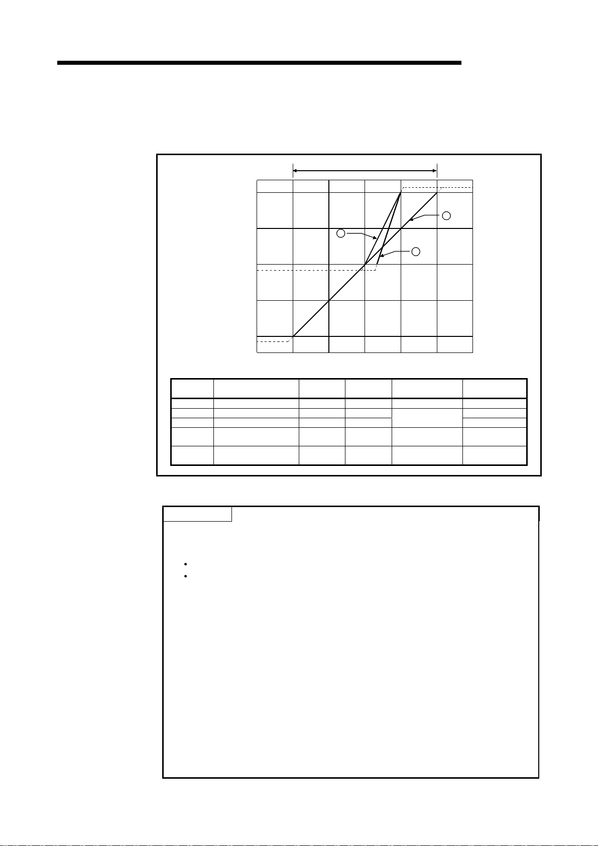
5
3.3.1 Voltage input characteristics
The voltage input characteristic graph is shown below.
Analog input parcitcal value
4095
4000
2000
0
-96
Digital output value
-2000
-4000
-4096
-15 -10 -5 0 5 10 1
2
3
1
Analog input voltage (V)
MELSEC-A
1
Number
1) -10 to +10V 0V 10V -4000 to +4000 2.5mV
2) 0 to 5V 0V 5V 1.25mV
3) 1 to 5V 1V 5V
—
—
Analog Input Range
Setting
User range setting 1
(-10 to +10V)
User range setting 2
(0 to 5V)
Offset
Value
0V 10V -4000 to +4000 2.5mV
0V 5V 0 to 4000 1.0mV
Gain
Value
Digital Output
Value*
0 to 4000
Maximum
Resolution
1.0mV
Fig. 3.1 Voltage Input Characteristic
POINT
(1) Do not input more than ±15V. The element may be damaged.
(2) If the anal og i np u t prov id ed co rre spo nd s to th e di gi tal ou tp ut val ue* bey on d it s
range, the digital output value is fixed to the maximum or minimum.
For 0 to 4000, the digital output value is within the range -96 to 4095.
For -4000 to +4000, the digital output value is within the range -4096 to +4095.
(3) Within the analog input and digital output scopes of each input range, the
maximum resolution and accuracy are within the performance specification
range. Outside those scopes, however, they may not fall within the performance
specification range. (Avoid using the dotted line part in Fig. 3.1.)
(4) Set the offset and gain values of the user range setting within the range
satisfying the fol low i ng cond itio n s.
(a) Setting ran ge when use r ra ng e se ttin g 1 is sele cted : - 1 0 to +10V
(b) Setting ran ge wh en use r ra nge se tt in g 2 is sele ct ed : 0 to 5V
(c) (Gain value) > (Offset value)
If you attempt to make setting outside the setting range of (a) or (b), the "RUN"
LED flickers at 0.5s intervals.
Set the values within the setting range.
If you attempt to make setting outside the setting range of (c), the "RUN" LED
flickers at 0.5s intervals.
Make setting again .
3 - 4
Page 20
3 SPECIFICATION
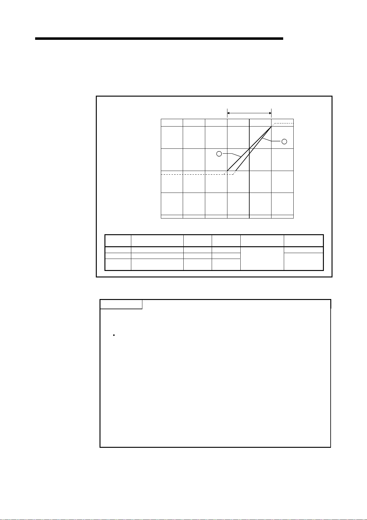
3.3.2 Current input characteristics
The current input characteristic graph is shown below.
4095
4000
2000
MELSEC-A
Analog input
parcitcal value
2
1
0
-96
Digital output value
-2000
-4000
-30 -20 -10 0 10 20 30
Number
1) 0 to 20mA 0mA 20mA 5µA
2) 4 to 20mA 4mA 20mA
—
Analog Input Range
Setting
User range setting 3
(0 to 20mA)
Analog input current (mA)
Offset
Value
0mA 20mA
Gain
Value
4
Digital Output
Value*
0 to 4000
Maximum
Resolution
4µA
Fig. 3.2 Current Input Characteristic
POINT
(1) Do not input more than ±30mA. A breakdown may result due to heat increase.
(2) If the anal og i np u t prov id ed co rre spo nd s to th e di gi tal ou tp ut val ue* bey on d it s
range, the digital output value is fixed to the maximum or minimum.
For 0 to 4000, the digital output value is within the range -96 to 4095.
(3) Within the analog input and digital output scopes of each input range, the
maximum resolution and accuracy are within the performance specification
range. Outside those scopes, however, they may not fall within the performance
specification range. (Avoid using the dotted line part in Fig. 3.2.)
(4) Set the offset and gain values of the user range setting within the range
satisfying the fol low i ng cond itio n s.
(a) Setting ran ge wh en use r ra nge se tt in g 3 is sele ct ed : 0 to 20mA
(b) (Gain value) > (Offset value)
If you attempt to make setting outside the setting range of (a), the "RUN" LED
flickers at 0.5s intervals.
Set the values within the setting range.
If you attempt to make setting outside the setting range of (b), the "RUN" LED
flickers at 0.5s intervals.
Make setting again .
3 - 5
Page 21
3 SPECIFICATION
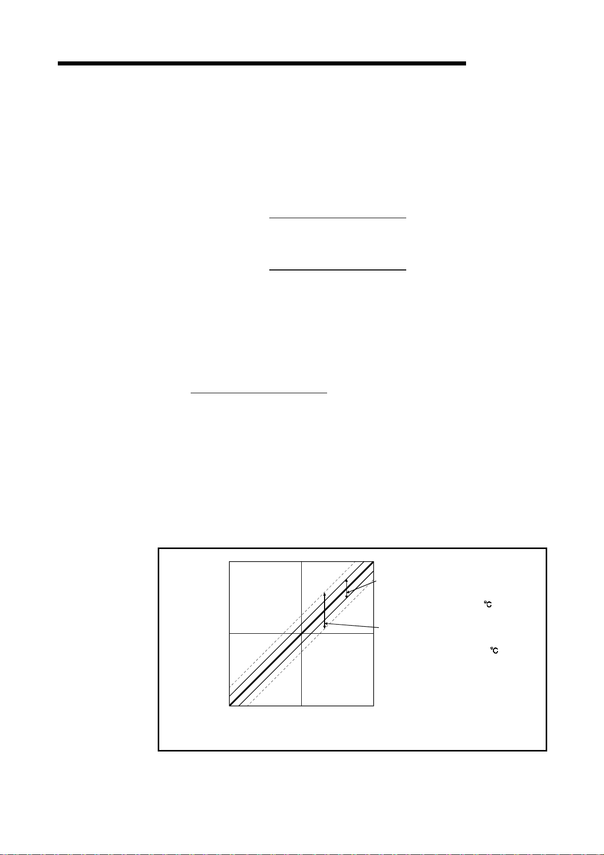
3.3.3 Relationship between the offset/gain setti ng and di g i tal output v al ue
The relationship between the offset/gain setting and digital output value is described.
(1) Resolution
The resolution is obtained by the following formula:
(a) For the voltage input:
MELSEC-A
3.3.4 Accuracy
Resolution =
(Gain value) - (Offset value)
4000
(b) For the current input:
Resolution =
(Gain value) - (Offset value)
4000
(2) Relationship between the max imum r esol uti on and di g i tal output
value
The maximum resolution of the AJ65SBT-64AD is as indicated in the
performance specification.
If the following is satisfied from the offset/gain setting, the digital output value
does not increases /decreases by one.
(Gain value) - (Offset value)
4000
Accuracy is relative to the maximum value of the digital output value.
If you change the offset/gain setting or input range to change the input characteristic,
accuracy does not change and is held within the range indicated in the performance
specifications.
Accuracy is within ±0.2% (±8 digit) at the operating ambient temperature of 25±5°C or
within ±0.4% (±16 digit) at the operating ambient temperature of 0 to 55°C.
< Maximum resolution
4000
Varies within the range of
±0.2% (±8 digit) at operating
ambient temperature of 25±5 .
0
Digital output value
-4000
-10V 10V
0V
Analog input value
Varies within the range of
±0.4% (±16 digit) at operating
ambient temperature of 0 to 55 .
Fig. 3.3 Voltage Input Characteristic Accuracy
3 - 6
Page 22
3 SPECIFICATION
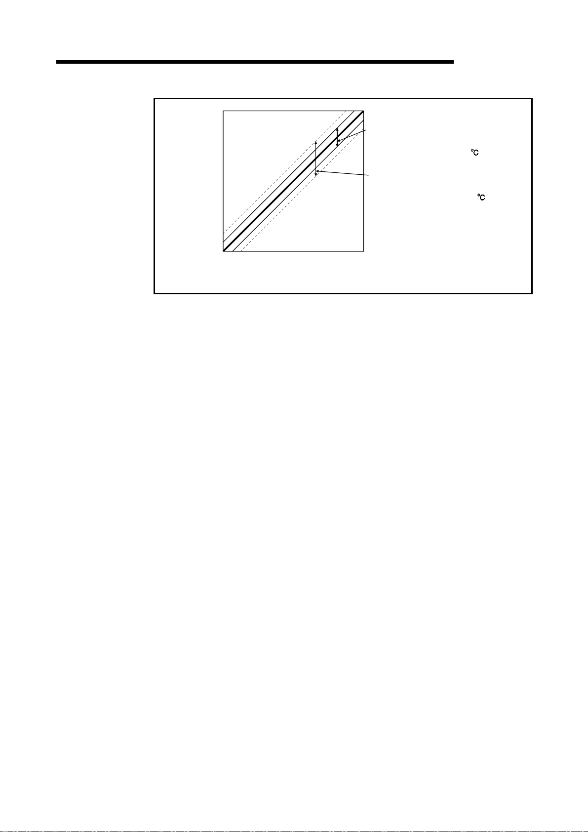
3.3.5 Conversion speed
4000
Varies within the range of
±0.2% (±8 digit) at operating
ambient temperature of 25±5 .
Varies within the range of
±0.4% (±16 digit) at operating
ambient temperature of 0 to 55 .
Digital output value
0
0
Analog input value
20mA
Fig. 3.4 Current Input Characteristic Accuracy
MELSEC-A
Conversion speed in di cat e s ti me fro m chan nel cha ngi ng to A/ D conv e rsio n co mpl etio n.
Conversion speed pe r cha n nel of t he AJ 65S B T-64AD is 1 ms.
Due to the data link processing time of the CC-Link system, there is a transmission
delay until the A/D conversion value is read actually.
For the data link processing time, refer to the user's manual of the master module
used.
Example) Data link processing time taken when the master module is the AJ61BT11 or
A1SJ61BT11
[Calculation expression]
SM+LS×2+remote device station processing time
SM: Scan time of master station sequence program
LS : Link scan time
Remote device station processing time: (Number of channels used+1*) × 1ms
*: Internal processing time of AJ65SBT-64AD
3 - 7
Page 23
3 SPECIFICATION
3.4 Function List
Item D e scription Refer to
Sampling processing
Moving average
processing
A/D conversion
enable/prohibit
specification
Input range changing
function
The AJ65SBT-64AD function list is shown in table 3.3.
Table 3.3 AJ65SBT-64AD function list
Perform A/D conversion of an analog input value one by one and store the result into
the remote register each time.
Average the digital output values of the specified count measured per sampling time.
Specify whether A/D conversion is enabled or disabled per channel.
By prohibiting the conversion for the channels which are not used, the sampling time
can be shortened.
Can set the analog input range per channel to change the I/O conversion
characteristics.
Select the input range setting from among the following 8 types.
Input Range Set Value
-10 to +10V 0H
0 to 5V 1H
1 to 5V 2H
0 to 20mA 3H
4 to 20mA 4H
User range setting 1 (-10 to +10V) 5H
User range setting 2 (0 to 5V) 6H
User range setting 3 (0 to 20mA) 7H
MELSEC-A
Section 3.4.1
Section 3.5.2
Section 3.4.2
Section 3.5.2
Section 3.6.4
Section 3.6.2
Section 3.6.3
Offset/gain setting
The offset/gain setting can be performed volumeless for each channel, and the I/O
conversion characteristics can be changed.
Section 4.4
3 - 8
Page 24
3 SPECIFICATION
3.4.1 Sampling processing
The A/D conver sion is per fo rmed su cce ssively for the analog inp ut , and the con v er te d
digital output values are stored in the remote register.
The processing time to store the digital output value into the remote register after the
sampling pro ce ssi ng differs dependi ng on th e nu mbe r o f A/ D co nve rsio n en ab le d
channels.
(Processing time) Number of A/D conversion enabled channels) 1 (ms)
[Example] When three channels, channels 1, 2, and 3 are enabled for conversion:
3×1 = 3 (ms)
3.4.2 Moving average processing
The specified coun t of di gi ta l ou tpu t val ue s imported per sampli ng ti me a re ave rag ed to
find a value, which is then stored into the remote register.
Since average processing is performed with data shifted per sampling, the most recent
digital output value is available.
Average processing can be performed without changing the conversion speed.
Use moving average processing count setting (address RWwm+2) to set the number
of moving average processings.
The count can be selected from among four types: 4, 8, 16 and 32 times.
MELSEC-A
Maximum conversion speed
Moving average processing at the count setting of 4 times
6
2 3
+ + +
Sampling time
8
7
5
4
A/D conversion value
4000
2000
3
2
1
0
Data transition inside remote register
Stored first time
2 3
1
+ + +
4 4 4
4
5
A/D conversion completion flag ON
Stored second time Stored third time
4
9
10 11
Stored first time
Stored second time
Stored third time
3
4
+ + +
12
Remote register
Digital output value
Time [ms]
65
3 - 9
Page 25
3 SPECIFICATION
MELSEC-A
3.5 Remote I/O Signals
This section describes the assignment and functions of the remote I/O signals.
3.5.1 Remote I/O signal list
Remote inputs (RX) mean the input signals from the AJ65SBT-64AD to the master
module, and remote outputs (RY) mean the output signals from the master module to
the AJ65SBT-64AD.
In communications with the master station, the AJ65SBT-64AD uses 32 points of the
remote inputs (RX) and 32 points of the remote outputs (RY). Table 3.4 indicates the
assignment and names of the remote I/O signals.
Table 3.4 Remote I/O Signals List
Signal direction: AJ65SBT-64AD Master Module Signal direction: Master Module AJ65SBT-64AD
Remote input (RX) Signal name Remote output (RY) Signal name
RXn0 CH.1 A/D conversion completion flag RYn0
RXn1 CH.2 A/D conversion completion flag RYn1
RXn2 CH.3 A/D conversion completion flag RYn2
RXn3 CH.4 A/D conversion completion flag RYn3
RXn4 CH.1 range error flag
RXn5 CH.2 range error flag
RXn6 CH.3 range error flag
RXn7 CH.4 range error flag
RXn8
to
RXnB
RXnC
RXnD
RXnE
RXnF Test mode flag
RX(n+1)0
to
RX(n+1)7
RX(n+1)8 Initial data processing request flag RY(n+1)8 Initial data processing completion flag
RX(n+1)9 Initial data setting completion flag RY(n+1)9 Initial data setting request flag
RX(n+1)A Error status flag RY(n+1)A Error reset request flag
RX(n+1)B Remote READY
RX(n+1)C
to
RX(n+1) F
Reserved
2
E
PROM write error flag
Reserved
Reserved
Reserved
RYn4
to
RY(n+1)7
RY(n+1)8
to
RY(n+1)F
CH.1 moving average processing
specifying flag
CH.2 moving average processing
specifying flag
CH.3 moving average processing
specifying flag
CH.4 moving average processing
specifying flag
Reserved
Reserved
POINT
The reserved devices given in Table 3.4 are used by the system and cannot be
used by the user.
If the user has used (turned on/off) any of them, we cannot guarantee the functions
of the AJ65SBT-64AD.
3 - 10
Page 26

3 SPECIFICATION
3.5.2 Functions of the remote I/O signals
Table 3.5 explains the functions of the remote I/O signals of the AJ65SBT-64AD.
Table 3.5 Remote I/O Signal Details (1/2)
Device No. Signal Name Description
The A/D conversion completion flag turns on at completion of the A/D conversion of
the corresponding channel when the initial data setting request flag (RY(n+1)9) turns
from off to on after power-on.
The A/D conversion completion flag processing is processed only once when the A/D
RXn0
to
RXn3
RXn4
to
RXn7
RXnC
RXnF Test mode flag
CH.
A/D Conversion
completion flag
CH.
E
range error flag
2
PROM write error flag
conversion enable/prohibit specification is changed.
When changing the A/D conversion from prohibit to enable:
When the average processing is specified, the flag turns on after completing the
average processing of the number of times or time, and storing the A/D conversion
digital value in the remote register.
When changing the A/D conversion from enable to prohibit:
The corresponding channel's A/D conversion completion flag turns off.
Turns on when the value set for input range setting is outside the setting range.
Turns on if all channels are not set to any of "user range settings 1 to 3" at offset/gain
setting (in the test mode).
Turns on if the number of E
channel). If this flag has turned on, this module itself has failed (hardware fault) and
therefore this flag cannot be reset (turned off) by the error reset request flag.
Turns on in the test mode.
(Used for interlock to prevent wrong output during offset/gain setting.)
After power-on, the initial data processing request flag is turned on by the AJ65SBT64AD to request the initial data to be set.
Also, after the initial data processing is complete (initial data processing completion
flag RY(n+1)8 ON), the flag is turned off.
2
PROM write times exceeds its limit (100,000 times per
MELSEC-A
RX(n+1)8
RX(n+1)9
Initial data processing
request flag
Initial data setting completion
flag
RX(n+1)8
Initial data processing request flag
RY(n+1)8
Initial data processing completion flag
RX(n+1)9
Initial data setting completion flag
RY(n+1)9
Initial data setting request flag
RX(n+1)B
Remote ready
RXn0 to RXn3
CH. A/D conversion completion flag
: Performed by sequence ladder
: Performed by AJ65SBT-64AD
When the initial data setting request (RY(n+1)9 ON) is made, the flag turns on after
the initial data setting completion is done.
Also, after the initial data setting is complete, the initial data setting completion flag
turns off when the initial data setting request flag turns off.
n: Address allocated to the master module by the station number setting.
3 - 11
Page 27

3 SPECIFICATION
MELSEC-A
Table 3.5 Remote I/O Signal Details (2/2)
Device No. Signal Name Description
RX(n+1)A Error status flag
RX(n+1)B Remote READY
RYn0
to
RYn3
RY(n+1)8
RY(n+1)9
RY(n+1)A Error reset request flag
CH.
processing specifying flag
Initial data processing
completion flag
Initial data setting request
flag
moving average
Turns on when CH.
(RXnC) has turned on.
Does not turn on at occurrence of the watchdog timer error. ("RUN" LED goes off.)
Turns on when initial data setting is completed after power-on or at termination of the
test mode.
(Used for interlocking read/write from/to the master module.)
Set the A/D conversion system to sampling processing or moving average
processing per channel.
Made valid on the leading edge of the initial data processing completion flag
(RY(n+1)8) or initial data setting request flag (RY(n+1)9).
OFF: Sampling processing
ON: Moving average processing
Turns on after initial data processing completion when initial data processing is
requested after power-on or test mode operation.
Turns on at the time of initial data setting or changing.
When this flag turns on, the CH.
off) and the error status flag (RX(n+1)A) is also reset, but the E
flag (RXnC) cannot be rest and therefore the error status flag remains on.
range error flag (RXn4 to RXn7) or E
RX(n+1)A
Error status flag
RXn4 to RXn7
CH. range error flag
RY(n+1)A
Error reset request flag
: Performed by sequence ladder
: Performed by AJ65SBT-64AD
range error flag (RXn4 to RXn7) is reset (turned
2
PROM write error flag
2
PROM write error
n: Address allocated to the master module by the station number setting.
3 - 12
Page 28

3 SPECIFICATION
MELSEC-A
3.6 Remote Register
The AJ65SBT-64AD has a remote resister for data communication with the master
module. The remote register allocation and data structures are described.
3.6.1 Remote register allocation
The remote regist e r all ocat i on i s sh own in Tabl e 3. 6 .
Table 3.6 Remote register allocati on
Communication direction Address Description Default value Reference section
RWwm A/D conversion enable/prohibit specification 0 Section 3.6.2
Master Remote
Remote Master
RWwm+1 Input range setting 0 Section 3.6.3
RWwm+2 Moving average processing count setting 0 Section 3.6.4
RWwm+3 Reserved 0 ——
RWrn CH.1 digital output value 0
RWrn+1 CH.2 digital output value 0
RWrn+2 CH.3 digital output value 0
RWrn+3 CH.4 digital output value 0
Section 3.6.5
m, n: Address allocated to the master module by the station number setting.
POINT
Do not read or write data from or to the reserved area of the remote register. If data
is read or written, we cannot guarantee the functions of the AJ65SBT-64AD.
3 - 13
Page 29

3 SPECIFICATION
3.6.2 A/D conversion enable/prohibit speci fication ( Addr ess RWwm)
(1) Set whether A/D conv e r sion is en abl ed o r disab le d pe r chann el .
(2) By setting the unused channels to conversion prohibit, the sampling cycle can be
shortened.
Example) The sampling cycle when only channels 1 and 3 are set to A/D
conversion enabled:
2 (Number of channels enabled) × 1ms (Conversion speed at one channel) = 2ms
(3) Operation is performed according to the setting made for the leading edges of
initial data setting request flag (RY(n+1)9).
(4) The defaul t set tin g i s A/ D conv e r sion di sa bl e fo r all cha nn els.
b15 b14 b13 b12 b11 b10 b9 b8 b7 b6 b5 b4 b3 b2 b1
MELSEC-A
b0
CH.3CH.4
CH.2 CH.1
Ignored
1: Enable A/D conversion
0: Prohibit A/D conversion
3 - 14
Page 30

3 SPECIFICATION
3.6.3 Input range setting (Address RWwm+1)
(1) Set the analog inpu t ra ng e pe r cha nn el .
(2) Operation is performed according to the setting made for the leading edges of the
initial data setting request flag (RY(n+1)9).
(3) The default setting is -10 to +10V for all channels.
b15 b12 b11 b8 b7 b4 b3 b0to
CH.4
Input Range Set Value
-10 to +10V 0H
0 to 5V 1H
1 to 5V 2H
0 to 20mA 3H
4 to 20mA 4H
User range setting 1 (-10 to +10V) 5H
User range setting 2 (0 to 5V) 6H
User range setting 3 (0 to 20mA) 7H
to
CH.3
to
CH.2
MELSEC-A
to
CH.1
(4) When making offset/gain setting, set all channels to any of "user range settings 1
to 3".
Setting any othe r rang e wi ll re sul t in an err o r and fli cke r t he "R UN" LE D at 0. 1 s
intervals.
3 - 15
Page 31

3 SPECIFICATION
3.6.4 Moving average processing count setting ( Addr ess RWwm+2)
(1) Set the average processing count of the channel for which moving average
processing has been specified in the CH.
specifying flag (RYn0 to RYn3).
moving average processing
MELSEC-A
3.6.5 CH.
(2) Sampling processing is performed for the channel whose CH.
processing specifying flag (RYn0 to RYn3) was not turned on, independently of
the moving average processing count setting.
(3) Operation is performed according to the setting made for the leading edges of the
initial data setting request flag (RY(n+1)9).
(4) The default setting is 4 times for all channels.
Bits b2, b3, b6, b7 , b1 0, b1 1 , b14 an d b1 5 a re ign o red .
b15 b12 b11 b8 b7 b4 b3 b0
b14 b13 b10 b9 b6 b5
Ignored Ignored Ignored Ignored
Digital output value (
moving average
b2
b1
CH.4 CH.3 CH.2 CH.1
Set Count Set Value
4 times 0H
8 times 1H
16 times 2H
32 times 3H
Address RWrn to RWrn+3
)
(1) The digital value after the A/D conversion is stored in the remote register address
from RWrn to RWrn+3 for each channel.
(2) The digital ou tp ut v alue i s exp resse d in a 16 -bi t en cod ed bin a ry.
b15 b14 b13 b12 b11 b10 b9 b8 b7 b6 b5 b4 b3 b2 b1 b0
Date section
b12 to b14 change to 1 when the sign is negative
(1 at b15) and to 0 when it is positive (0 at b15).
(A negative digital value is expressed in 2's complement.)
Sign bit
1: Negative
0: Positive
3 - 16
Page 32
4 SETUP AND PREPARATION BEFORE OPERATION
4 SETUP AND PREPARATION BEFORE OPERATION
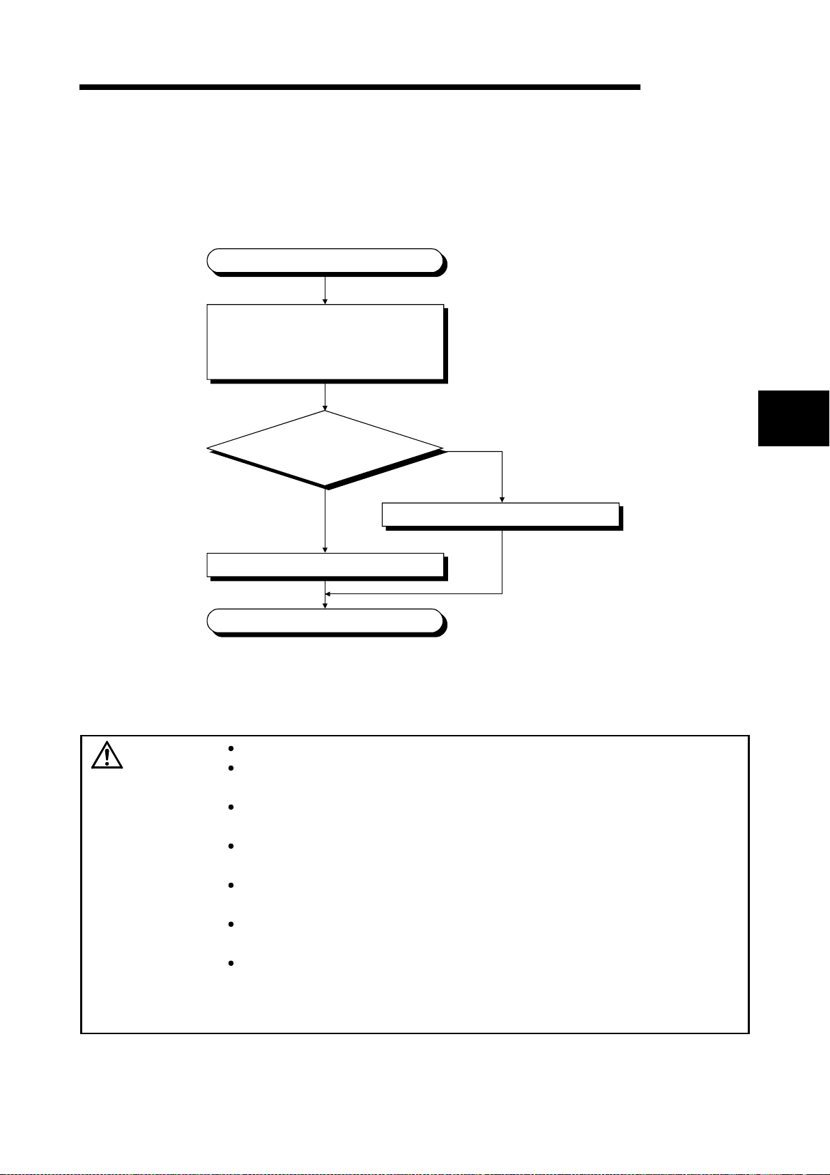
4.1 Pre-Operation Procedure
This section explains the preparatory procedure for operating the AJ65SBT-64AD.
START
Create a program.
(When making offset/gain setting, set all
channels to any of user range settings 1 to 3
in the sequence program.)
Make offset/gain setting?
.......Refer to Chapter 5.
No
MELSEC-A
4
Offset/gain setting (Refer to Section 4.4.)
4.2 Precautions When Handling
The precautions when handling the AJ65SBT-64AD are described below:
CAUTION
Do not touch the terminals while power is on. Doing so can cause a malfunction.
Ensure that no foreign matter such as chips and wire-offcuts enter the module.
Foreign matter can cause a fire, failure or malfunction.
Do not disassemble or modify the module.
Doing so can cause a failure, malfunction, injury or fire.
Do not touch the conductive and electronic parts of the module directly.
Doing so can cause the module to malfunction or fail.
Do not drop the module or give it hard impact since its case is made of resin.
Doing so can damage the module.
Do not touch the conductive parts of the module directly.
Doing so can cause the module to malfunction or fail.
Tighten the terminal screws within the specified torque range.
Undertightening can cause a short circuit or malfunction.
Overtightening can cause a short circuit or malfunction due to damage of the
screws or module.
Yes
Start data link.
END
4 - 1
Page 33
4 SETUP AND PREPARATION BEFORE OPERATION
MELSEC-A
CAUTION
Dispose of the product as industrial waste.
Use the module in the environment indicated in the general specifications given in
this manual.
Not doing so can cause an electric shock, fire, malfunction, product damage or
deterioration.
Securely fix the module to a DIN rail or with mounting screws, and securely tighten
the mounting screws within the specified torque range.
Undertightening can cause a drop or malfunction.
Overtightening can cause a drop or malfunction due to damage of the screws or
module.
Mount or dismount the module to or from an enclosure after switching power off
externally in all phases. Not doing so can cause the module to fail or malfunction.
(1) Perform the tightening of the module installation screws and terminal screws in the
following range.
Screw Location Tightening Torque Range
Module mounting screw (M4 screw) 78 to 108N cm
Terminal block terminal screw (M3 screw) 59 to 88N cm
Terminal block mounting screw (M3.5 screw) 68 to 98N cm
(2) When using the DIN rail adapter, install the DIN rail by making sure of the
following:
(a) Applicable DIN rail models (conforming to the JIS-C2B12)
TH35-7.5Fe
TH35-7.5Al
(b) DIN rail installation screw interval
When installing the DIN rail, tighten the screws with less than 200mm (7.87
inch) pitches.
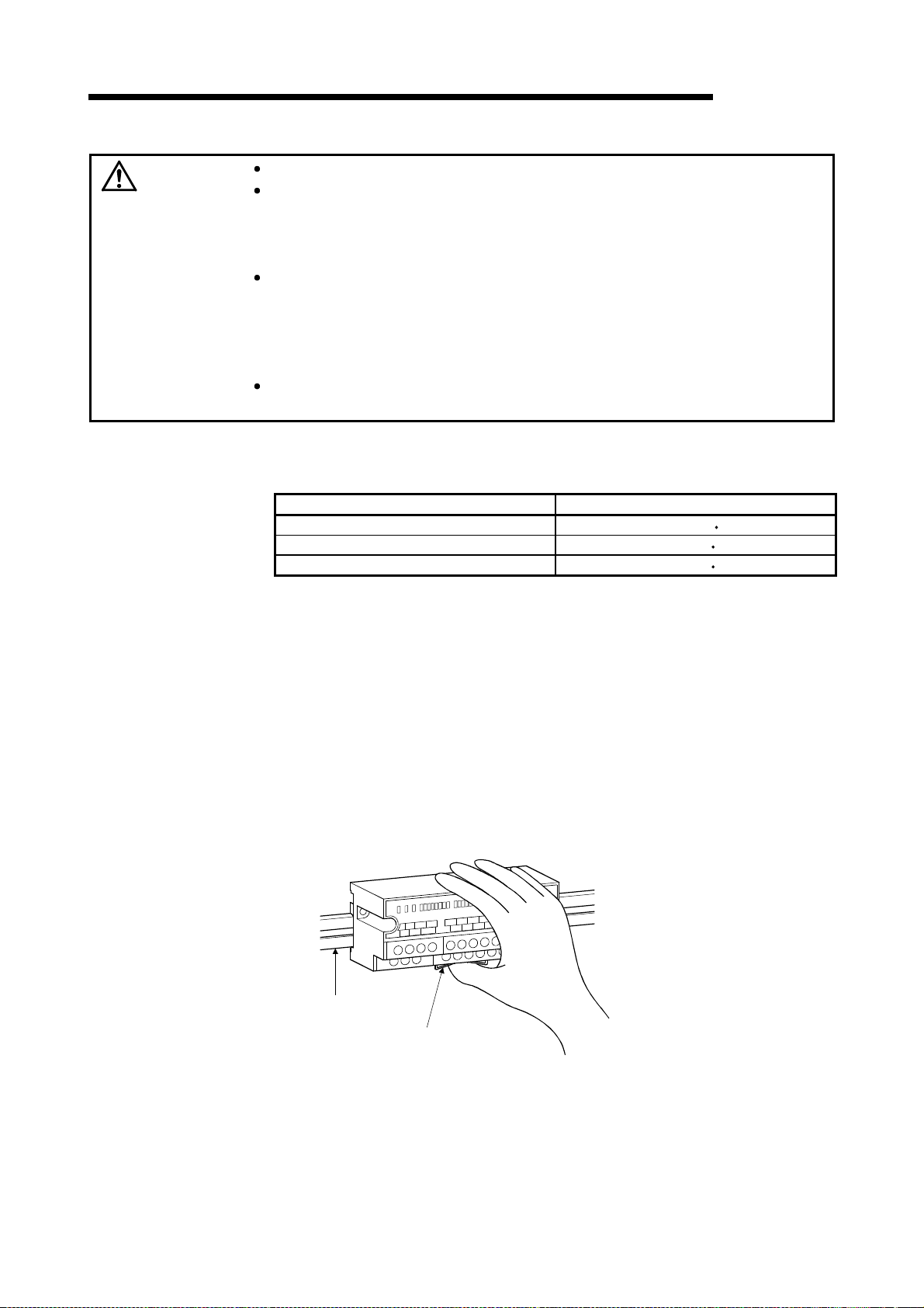
(3) When mounting the AJ65SBT-64AD to the DIN rail, press with your finger the
centerline of the DIN rail hook at the bottom of the module until it clicks.
DIN rail
DIN rail hook
(4) Refer to the Master Module user's manual for the name, specification, and
manufacturers of supported cables for the use with AJ65SBT-64AD.
4 - 2
Page 34
4 SETUP AND PREPARATION BEFORE OPERATION
2
c
s
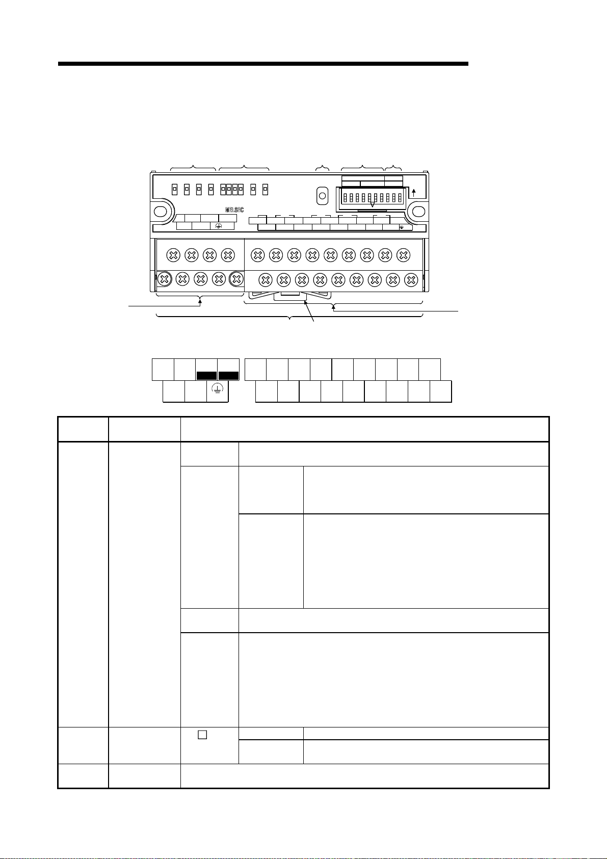
4.3 Name of Each Part
The name of each part in the AJ65SBT-64AD is shown.
MELSEC-A
1)
PW RUN L RUN L ERR. CH1 2 OFFSET GA IN
MITSUBISHI A
DA DG +24V 24G
DB SLD (FG)
-piece
(CC-Link
ommunication
ection)
[Terminal numbers and signal names]
1357
Number
1)
2)
3)
DA DG
Name and
appearance
Operation status
display LED
Offset/gain
adjusting LEDs
SELECT/SET
switch
246
+24V
DB SLD
(FG)
PW LED
RUN LED
L RUN LED
L ERR. LED
CH
OFFSET
GAIN
Used to make offset/gain setting in the test mode.
34
2)
J65SBT-64AD
TEST
TEST
V+ I+
CH1 CH2
V+ I+
SLD
COM
3)
SELECT
SET
COM
4) 5)
STATION NO. B RATE
40 20 10 8 4 2 1 4 2 1
CH3 CH4
SLD
COM
V+ I+
COM
V+ I+
ON
AG
(FG1)
Direct-coupled
(Analog I/O section)
6)
7)
8 1012141618202224
24G
TEST
V+ I+ V+ I+ SLD AG
9 1113151719212325
TEST
SLDCOM COM V+ I+ V+ I+
COM COM
FG1
Description
ON : Power supply on
OFF: Power supply off
On : Normal operation
Normal mode
Flashing : 0.1s intervals indicate an input range setting error.
Off : 24VDC power supply shutoff or watchdog timer error
occurred.
On : Indicates that the SELECT/SET switch is in the SET
position.
Flashing : 0.1s intervals indicate that the input range setting is not
Test mode
any of "user range settings 1 to 3".
0.5s intervals indicate that you attempted to make
offset/gain setting outside the setting range.
Off : Indicates that the SELECT/SET switch is in th e
SELECT or center position.
On : Normal communication
Off : Communication cutoff (time expiration error)
On : Indicates that transmission speed setting or station number setting is
outside the range.
Flicker at fixed intervals : Indicates that transmission speed setting or station
number setting was changed from that at power-on.
Flicker at unfixed intervals : Indicates that you forgot fitting the termination resistor or
the module or CC-Link dedicated cable is affected by
noise.
Off : Indicates normal communications.
Normal mode Normally OFF.
Test mode
The LEDs lit change every time the SELECT/SET switch is moved
to SELECT. (Refer to Section 4.4.)
4 - 3
Page 35
4 SETUP AND PREPARATION BEFORE OPERATION
MELSEC-A
Number
4)
Name and
appearance
Station number
setting switches
Description
Use the switches in STATION NO. "10", "20" and "40" to set the tens of the station number.
Use the switches in STATION NO. "1", "2", "4" and "8" to set the units of the station number.
The switches are all factory-set to OFF.
Always set the station number within the range 1 to 64.
Setting any other number than 1 to 64 will result in an error, flickering the "L ERR." LED.
You cannot set the same station number to two or more stations.
Tens UnitsStation
Number
1 OFF OFF OFF OFF OFF OFF ON
2 OFF OFF OFF OFF OFF ON OFF
3 OFF OFF OFF OFF OFF ON ON
4 OFF OFF OFF OFF ON OFF OFF
10 OFF OFF ON OFF OFF OFF OFF
11 OFF OFF ON OFF OFF OFF ON
64 ON ON OFF OFF ON OFF OFF
(Example) To set the station number to "32", set the switches as indicated below.
Number
32 OFF ON ON OFF OFF ON OFF
40 20 10 8 4 2 1
Tens UnitsStation
40 20 10 8 4 2 1
Set Value
0 OFF OFF OFF 156kbps
Transmission
5)
6) Terminal block Used to connect the module power supply, transmission and I/O signals.
7) DIN rail hook Used to mount the module to the DIN rail.
speed setting
switches
Always set the transmission speed within the above range.
The switches are all factory-set to OFF.
Making any other setting than the above will result in an error, flickering the "L ERR." LED.
1 OFF OFF ON 625kbps
2 OFF ON OFF 2.5Mbps
3 OFF ON ON 5.0Mbps
4 ON OFF OFF 10Mbps
421
Setting Switches
Transmission
Speed
4 - 4
Page 36
4 SETUP AND PREPARATION BEFORE OPERATION
4.4 Offset/Gain Setting
When changing the I/O conversion characteristics, follow the procedure below.
START
Move the SELECT/SET switch to "SET". Confirm that
Set all channels to any of "user range settings 1 to 3"
in the sequence program.
Short the TEST terminals (across 8-9) to enter the
test mode.
TEST
TEST
Power ON
the "RUN" LED is lit* and release your hand.
Change the lit offset/gain adjusting LEDs with the
SELECT/SET switch, and make sure that the LED of
the channel whose offset/gain will be set and the
"GAIN" LED are lit.
RUN SELECT
CH.1 2
SET
Lit
3 4 OFFSET GAIN
MELSEC-A
Start data link.
Make sure that the "RUN" LED is off.
A
Every time the SELECT/SET switch is moved to
"SELECT", the offset/gain adjusting LEDs lit change
as shown below.
CH1 offset
value setting
CH1 gain
value setting
CH2 offset
value setting
CH2 gain
value setting
Change the lit offset/gain adjusting LEDs with the
SELECT/SET switch, and make sure that the LED
of the channel whose offset/gain will be set and the
"OFFSET" LED are lit.
CH.1 2
Lit Lit
3 4 OFFSET GAINCH.1 2
34OFFSET GAIN
Lit
Lit
Add the voltage or current that will be the gain value.
For voltage
For current
V
V+
COM
V+
COM
I+
A
Move the SELECT/SET switch to "SET". Confirm that
the "RUN" LED is lit* and release your hand.
RUN SELECT
SET
Lit
Adjust other channels?
NO
YES
A
Open the TEST terminals (across 8-9).
Add the voltage or current that will be the offset value.
For voltage
For current
V
V+
COM
V+
COM
I+
A
The "RUN" LED is lit.
*: If the "RUN" LED is not lit, E2PROM may have failed. For details, refer to Section 6.1.
4 - 5
TEST
TEST
Power OFF
END
Page 37

4 SETUP AND PREPARATION BEFORE OPERATION
POINT
(1) Set the offset and gain values in the actual usage state.
(2) The offset and gain values are stored on E
are not cleared at power-off.
(3) Shorting the TEST terminals to enter the test mode and executing initial settings
will start A/D conversion on all channels. To judge the test mode, use the test
mode flag as an interlock.
(4) Make offset/gain setting within the range indicated in POINT of Section 3.3.1
and Section 3.3.2. If setting is made outside this range, the maximum
resolution/accuracy may not fall within the performance specifications range.
(5) When making offset/gain setting (in the test mode), set all channels to any of
"user range settings 1 to 3".
Setting any other range will result in an error and flicker the "RUN" LED at 0.1s
intervals.
Refer to Section 3.6.3 for input range setting.
(6) When the grounding indicated in Section 4.8.2 *5 is changed (not performed
perform, or performed to removed), repeat the offset/gain setting from the start.
MELSEC-A
2
PROM in the AJ65SBT-64AD and
4 - 6
Page 38

4 SETUP AND PREPARATION BEFORE OPERATION
4.5 Station Number Setting
The station number setting of the AJ65SBT-64AD determines the buffer memory
addresses of the master module where the remote I/O signals and read/write data are
stored.
For details, refer to the user's manual of the master module used.
4.6 Facing Direction of the Module Installation
The AJ65SBT-64AD module may be installed in any of six directions.
(There are no restrictions on the facing directions.)
Also, a DIN rail may be used for installation.
Ceiling installation
MELSEC-A
DIN rail
Front installatio n
Flat installation
4 - 7
Page 39
4 SETUP AND PREPARATION BEFORE OPERATION
4.7 Data Link Cable Wiring
This section explains the wiring of the CC-Link dedicated cable used for connection of
the AJ65SBT-64AD and master module.
4.7.1 Instructions for handling the CC-Li nk dedicated cabl es
Do not handle the CC-Link dedicated cables roughly as described below. Doing so can
damage the cables.
Compact with a sharp object.
Twist the cable excessiv ely .
Pull the cable hard. (more than the permitted elasticity.)
Step on the cable.
Place an object on the top.
Scratch the cable's protective layer.
4.7.2 Connection of the CC-Link dedicated cables
MELSEC-A
Connect the CC-Link dedicated cable between the AJ65SBT-64AD and master
module as shown below.
Master module side
Termination resistor
4.8 Wiring
This section provides the instructions for wiring the AJ65SBT-64AD and its wiring with
external equipment.
4.8.1 Wiring precautions
To obtain maximum performance from the functions of AJ65SBT-64AD and improve
the system reli ab ili ty , an e xte rnal wi ri ng wi th hig h du rab ili ty agai n s t noise is required.
The precautions when performing external wiring are as follows:
(1) Use separa te cabl e s for t he AC and AJ65SBT-64AD ext e rnal input signals, in
AJ65SBT-64AD I/O module or like
DA
DB
DG
SLD
FG
CC-Link dedicated
cable
DA
DB
DG
SLD
CC-Link dedicated
FG
cable
DA
DB
DG
SLD
FG
order not to be affected by the AC side surge or conductivity.
Termination resistor
(2) Do not bundle or place with load carrying wires other than the main circuit line,
high voltage line or PLC. Noises, surges, or conductivity may affect the system.
(3) Place a one-poi nt grou nd in g on th e PL C side fo r the shie ld ed line or shielded
cable. However, depending on the external noise conditions, it may be better have
a grounding externally.
4 - 8
Page 40
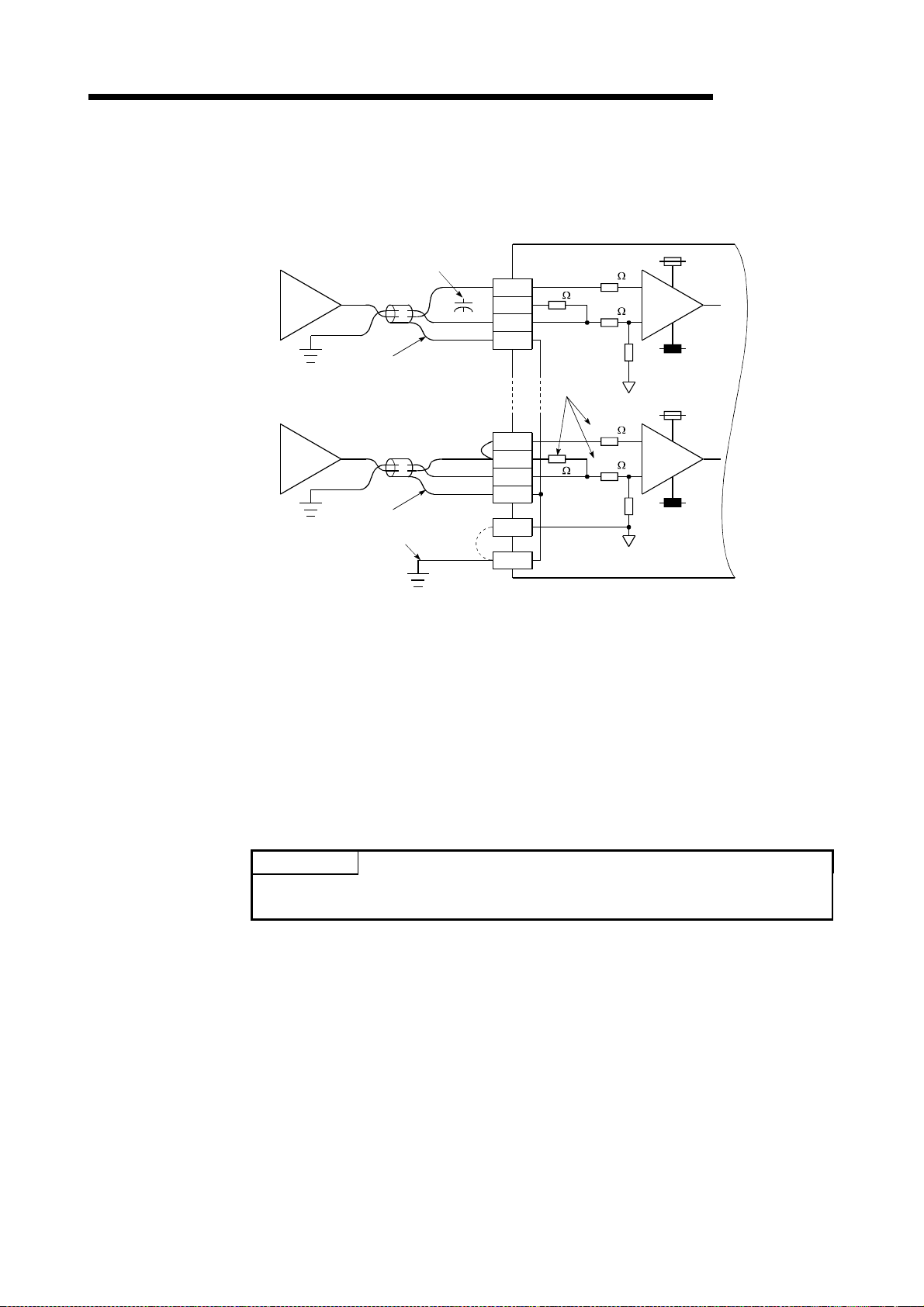
4 SETUP AND PREPARATION BEFORE OPERATION
4.8.2 Module connection example
For voltage input
MELSEC-A
Signal source 0 to ±10 V
For current input
Signal source 0 to ±20mA
*1 Shield
*1 Shield
*5
*4
CH1
V+
250
I+
COM
SLD
CH4
V+
*3
I+
250
COM
SLD
AG
FG1
500k
500k
*2
GND
500k
500k
+15V
-15V
*1 Use a two-core twisted shield line for the power cable.
*2 Indicates the AJ65SBT-64AD input resistor.
*3 For the current input, be sure to connect the (V+) and (I+) terminals.
*4 When noise or ripple occurs with the external cable, connect a condenser with
about 0.1 to 0.47µF (25V or higher voltage-resistant product) between the terminal
V and COM.
*5 Always perform grounding for FG1. When there is a lot of noise, it may be better
ground AG as well.
If the grounding wiring (grounding yes/no) is changed after the offset and gain are
set, perform the setting of the offset/gain values again.
POINT
A/D conversion values are fluctuated by self-heating within approx. 30 minutes after
power is turned ON.
4.9 Maintenance and Inspection
There are no special inspection items for the AJ65SBT-64AD module, but follow the
inspections items describes in the PLC CPU User's Manual so that the system can
always be used in the best condition.
4 - 9
Page 41

4 SETUP AND PREPARATION BEFORE OPERATION
MEMO
MELSEC-A
4 - 10
Page 42

5 PROGRAMMING
5 PROGRAMMING
The programming procedure, basic read/write programs, and program examples for
the AJ65SBT-64AD are described.
Refer to Section 3.6 for the remote registers and to the AnSHCPU/AnACPU/AnUCPU/
QCPU-A (A Mode) programming manual (dedicated instructions) for details of the
dedicated instructions.
5.1 Programming Procedure
Create a program which executes the AJ65SBT-64AD analog/digital conversion by
following the procedure below:
A/D conversion enable/prohibit specification
MELSEC-A
START
Input range setting
Perform moving average processing?
Yes
Moving average processing count setting
Specify the channel for which moving average
processing will be performed.
Read digital output value read
END
5
No
5 - 1
Page 43
5 PROGRAMMING
MELSEC-A
5.2 Program Examples
This section provides the program examples of the AJ65SBT-64AD.
5.2.1 Program examples for use of the ACPU /QC PU ( A mode) ( FR OM /TO instr uctions)
The program examples in this section are created under the following conditions.
A sequence program is used to set the network parameters.
[Relationships between PLC CPU, master module and AJ65SBT-64AD]
PLC CPU
Device X
X100 to X10F
X110 to X11F
Device Y
Y100 to Y10F
Y110 to Y11F
Address
E0
E1
160
161
Master module
Remote input (RX)
H
RX00 to RX0F
H
RX10 to RX1F
Remote output (RY)
H
RY00 to RY0F
H
RY10 to RY1F
AJ65SBT-64AD
(Station number 1)
Remote input (RX)
RX00 to RX0F
RX10 to RX1F
Remote output (RY)
RY00 to RY0F
RY10 to RY1F
Device D
D200
D201
D202
D203
Device D
D300
D301
D302
D303
Remote register (RWw)
H
1E0
1E1
1E2
1E3
H
H
H
RWw0
RWw1
RWw2
RWw3
Remote register (RWr)
H
2E0
H
2E1
H
2E2
H
2E3
RWr0
RWr1
RWr2
RWr3
Remote register (RWw)
RWw (A/D conversion
enable/prohibit specification)
RWw1 (Input range setting)
RWw2 (Moving average processing
count setting)
RWw3 (Reserved)
Remote register (RWr)
RWr (CH.1 digital output value)
RWr1 (CH.2 digital output value)
RWr2 (CH.3 digital output value)
RWr3 (CH.4 digital output value)
[Initial settings]
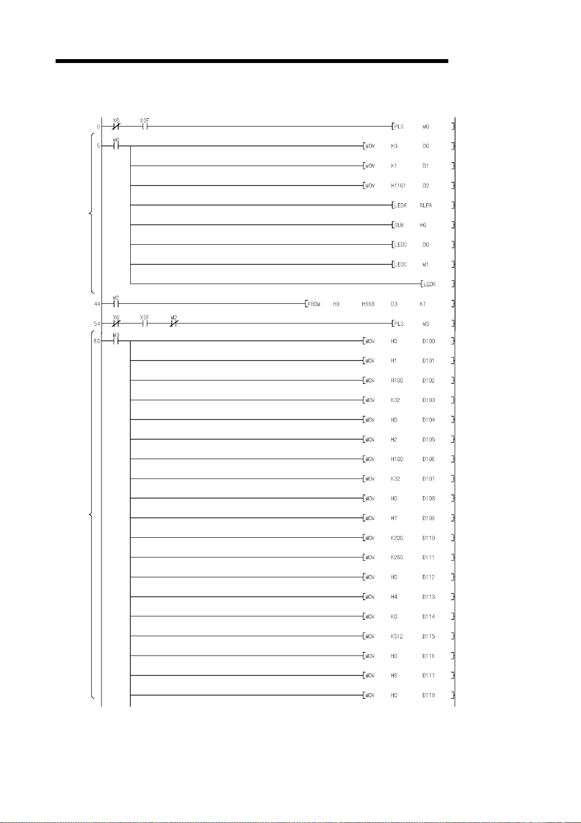
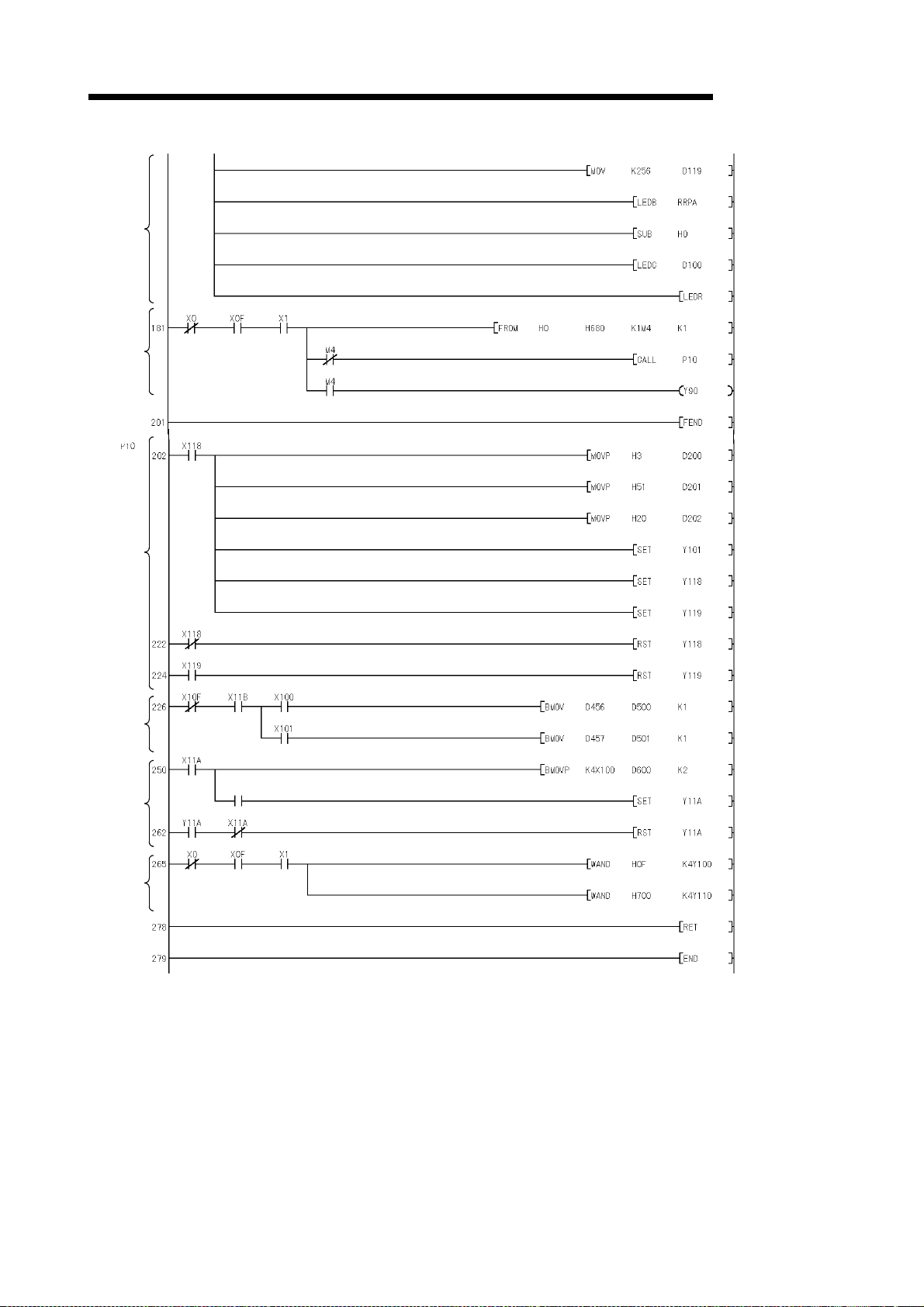
A/D conversion enabled channels.................Channels 1, 2
Moving average processing channel.............Channel 2 count setting = 16 times
Input range setting .........................................Channel 1: 0 to 5V
Channel 2: User range setting 1
5 - 2
Page 44

5 PROGRAMMING
Initial
settings of
master
station
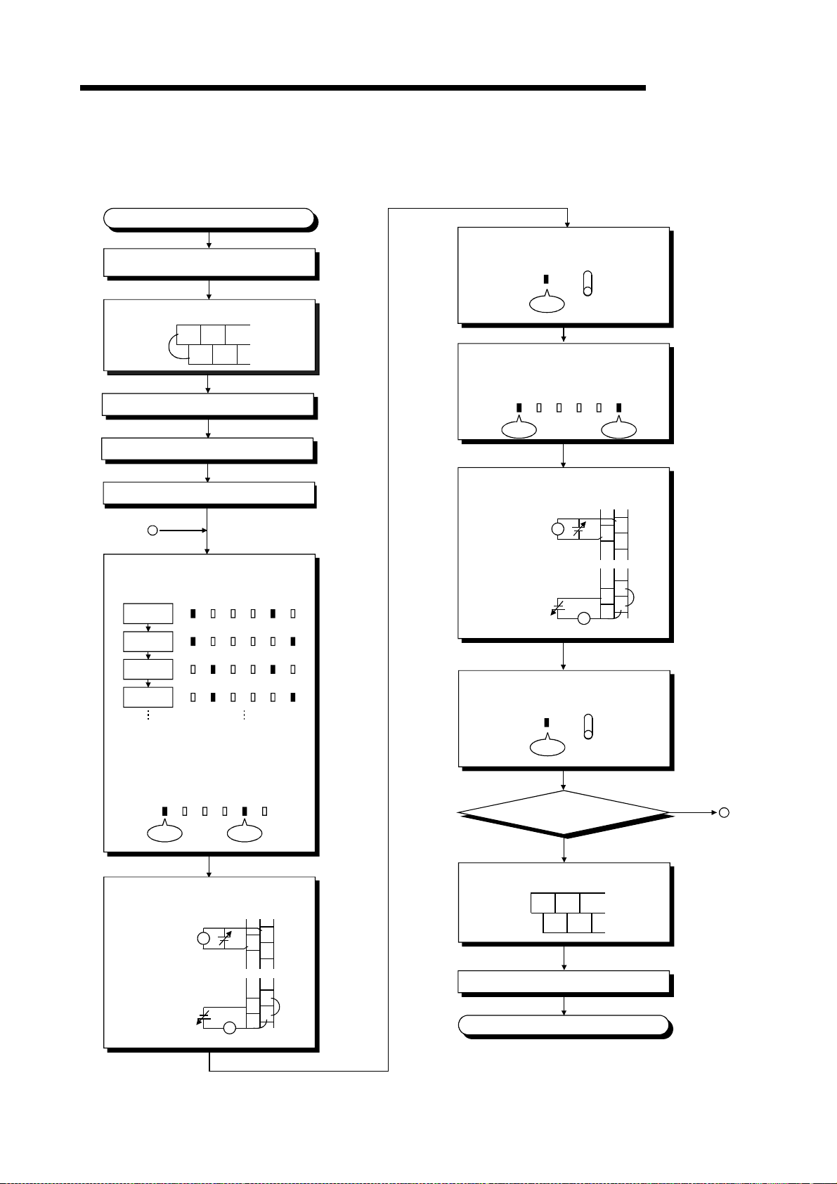
Read of
remote
input
signals
Checking
of
AJ65SBT64AD
status
(1) Program example for pow er - on
Error LED
MELSEC-A
Number of connected
modules: 1
Writes to master station
AJ65SBT-64AD station
information (remote device
station, 1 station occupied,
station No. 1)
Writes to master station
Refresh directive
Data link started by
buffer memory
Turns off start request
signal at normal completion
of start.
Reads parameter status at
abnormal completion of start.
Turns off start request signal
at abnormal completion of start.
RXn0 to RX(n+1)F are read to
X100 to X11F
Reads data link status.
AJ65SBT-64AD data link
normal
AJ65SBT-64AD data link
abnormal
Initial
settings
Read of
digital
values
CH.1, CH.2: A/D conversion
enabled
CH.1: 0 to 5V
CH.2: User range setting 1
CH.2 moving average
processing count: 16 times
Writes to master station.
Turns on CH.2 moving average
processing specifying flag.
Turns on initial data processing
completion flag.
Turns on initial data setting
request flag.
Turns off initial data processing
completion flag.
Turns off initial data setting
request flag.
Reads CH.1 digital value.
Reads CH.2 digital value.
5 - 3
Page 45

5 PROGRAMMING
Processing
at error
occurrence
Masks
disabled
devices.
Write of
remote
output
signals
User designation
MELSEC-A
Reads error.
Turns on error reset
request flag.
Turns off e rror reset
request flag.
Masks RY100 to RY10F
disabled devices.
Masks RY110 to RY11F
disabled devices.
Y100 to Y11F are written
into RYn0 to RY(n+1)F.
5 - 4
Page 46

5 PROGRAMMING
Initial
settings of
master
station
Read of
remote
input
signals
Checking
of
AJ65SBT
-64AD
status
(2) Program example for init ial data chang i ng
Error LED
MELSEC-A
Number of connected
modules: 1
Writes to master station
AJ65SBT-64AD station
information (remote device
station, 1 station occupied,
station No. 1)
Writes to master station
Refresh directive
Data link started by
buffer memor y
Turns off start request
signal at normal completion
of start.
Reads parameter status at
abnormal completion of start.
Turns off start request signal
at abnormal completion of start.
RXn0 to RX(n+1)F are read to
X100 to X11F.
Reads data link status.
AJ65SBT-64AD data link
normal
AJ65SBT-64AD data link
abnormal
Initial
settings
Read of
digital
values
User designatiion
CH.1, CH.2: A/D conversion
enabled
CH.1: 0 to 5V
CH.2: User range setting 1
CH.2 moving average
processing count: 16 times
Writes to master station.
Turns on CH.2 moving average
processing specifying flag.
Turns on initial data setting
request flag.
Turns off initial data setting
request flag.
Reads CH.1 digital value.
Reads CH.2 digital value.
5 - 5
Page 47

5 PROGRAMMING
n
Processing
at error
occurrence
Masks
disabled
devices.
Write of
remote
output
signals
User designation
MELSEC-A
Reads error.
Turns on error reset
request flag.
Turns off error reset
request flag.
Masks RY100 to RY10F
disabled devices.
Masks RY110 to RY11F
disabled devices.
Y100 to Y11F are writte
into RYn0 to RY(n+1)F.
5 - 6
Page 48
5 PROGRAMMING
MELSEC-A
5.2.2 Program examples for use of the ACPU /QC PU ( A mode) ( dedic ated instr ucti ons)
The program examples in this section are created under the following conditions.
A sequence program is used to set the network and automatic refresh parameters.
[Relationships between PLC CPU, master module and AJ65SBT-64AD]
PLC CPU
Device X
X100 to X10F
X110 to X11F
Device Y
Y100 to Y10F
Y110 to Y11F
Address
E0
E1
160
161
Master module
Remote input (RX)
H
RX00 to RX0F
H
RX10 to RX1F
Remote output (RY)
H
RY00 to RY0F
H
RY10 to RY1F
AJ65SBT-64AD
(Station number 1)
Remote input (RX)
RX00 to RX0F
RX10 to RX1F
Remote output (RY)
RY00 to RY0F
RY10 to RY1F
Device D
D200
D201
D202
D203
Device D
D456
D457
D458
D459
Remote register (RWw)
H
1E0
1E1
1E2
1E3
H
H
H
RWw0
RWw1
RWw2
RWw3
Remote register (RWr)
H
2E0
H
2E1
H
2E2
H
2E3
RWr0
RWr1
RWr2
RWr3
Remote register (RWw)
RWw (A/D conversion
enable/prohibit specification)
RWw1 (Input range setting)
RWw2 (Moving average processing
count setting)
RWw3 (Reserved)
Remote register (RWr)
RWr (CH.1 digital output value)
RWr1 (CH.2 digital output value)
RWr2 (CH.3 digital output value)
RWr3 (CH.4 digital output value)
[Initial settings]
A/D conversion enabled channels.................Channels 1, 2
Moving average processing channel.............Channel 2 count setting = 16 times
Input range setting .........................................Channel 1: 0 to 5V
Channel 2: User range setting 1
5 - 7
Page 49
5 PROGRAMMING
S
n
p
S
a
r
p
etting of
etwork
arameters
(1) Program example for pow er - on
MELSEC-A
Synchronization
mode invalid
Number of connected
modules:1
AJ65SBT-64AD station
informat io n (r em o t e
device station, 1 station
occupied, station No. 1)
Dedicated instruction
(RLPA)
Starting I/O number of
master module
Parameter storage
starting device
Device which turns on 1
scan at completion
Reads parameter status
at abnormal completion.
etting of
utomatic
efresh
arameters
Sets RX starting number.
Sets "X".
Sets X100.
Sets 32 points.
Sets RY starting number.
Sets "Y".
Sets Y100.
Sets 32 points.
Sets RW starting number.
Sets "D".
Sets D200.
Sets 260 points.
Sets SB starting number.
Sets "B".
Sets B0.
Sets 512 points.
Sets SW starting number.
Sets "W".
Sets W0.
5 - 8
Page 50
5 PROGRAMMING
Setting of
automatic
refresh
parameters
MELSEC-A
Sets 256 points.
Dedicated instruction
(RRPA)
Starting I/O number of
master module
Parameter storage
starting device
Checking
of AJ65SBT
-64AD status
Initial
settings
Read of
digital values
Processing
at error
occurrence
Masks
disabled
devices.
User designation
Error LED
Reads data link status.
AJ65SBT-64AD data
link normal
AJ65SBT-64AD data
link abnormal
CH.1, CH.2: A/D
conversion enabled
CH.1: 0 to 5V
CH.2: User range
setting 1
CH.2 moving average
processing count:
16 times
Turns on CH.2 moving
average processing
specifying flag.
Turns on initial data
processing completion
flag.
Turns on initial data
setting request flag.
Turns off initial data
processing completion
flag.
Turns off initial data
setting request flag.
Reads CH.1 digital
value.
Reads CH.2 digital
value.
Reads error.
Turns on error reset
request flag.
Turns off error reset
request flag.
Masks RY100 to
RY10F disabled
devices.
Masks RY110 to
RY11F disabled
devices.
5 - 9
Page 51
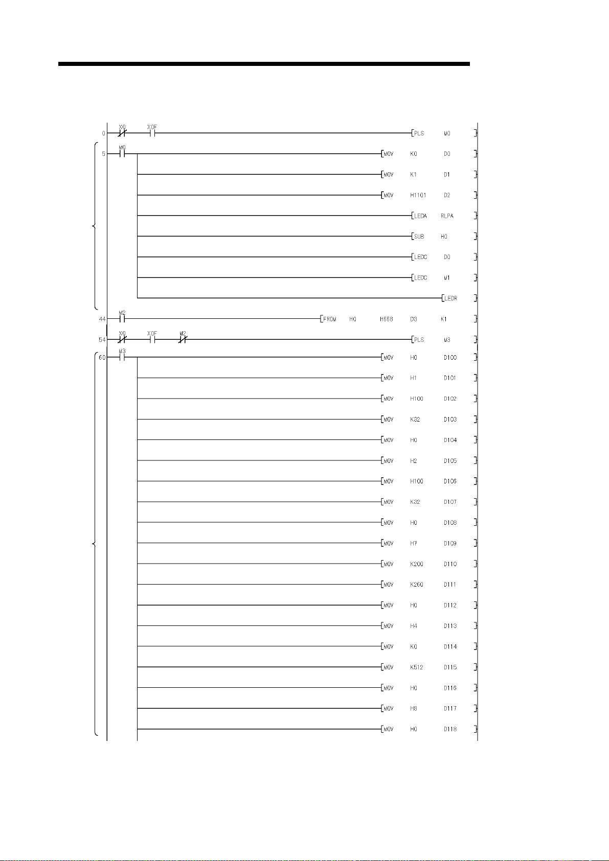
5 PROGRAMMING
.
.
Setting of
network
parameters
(2) Program example for init ial data chang i ng
MELSEC-A
Synchronization
mode invalid
Number of connected
modules:1
AJ65SBT-64AD station
information (remote
device station, 1 station
occupied, station No. 1)
Dedicated instruction
(RLPA)
Starting I/O number of
master module
Parameter storage
starting device
Device which turns on 1
scan at completion
Reads parameter status
at abnormal completion.
Setting of
automatic
refresh
parameters
Sets RX starting number.
Sets "X".
Sets X100.
Sets 32 points.
Sets RY starting number.
Sets "Y".
Sets Y100.
Sets 32 points.
Sets RW starting number
Sets "D".
Sets D200.
Sets 260 points.
Sets SB starting number.
Sets "B".
Sets B0.
Sets 512 points.
Sets SW starting number
Sets "W".
Sets W0.
5 - 10
Page 52
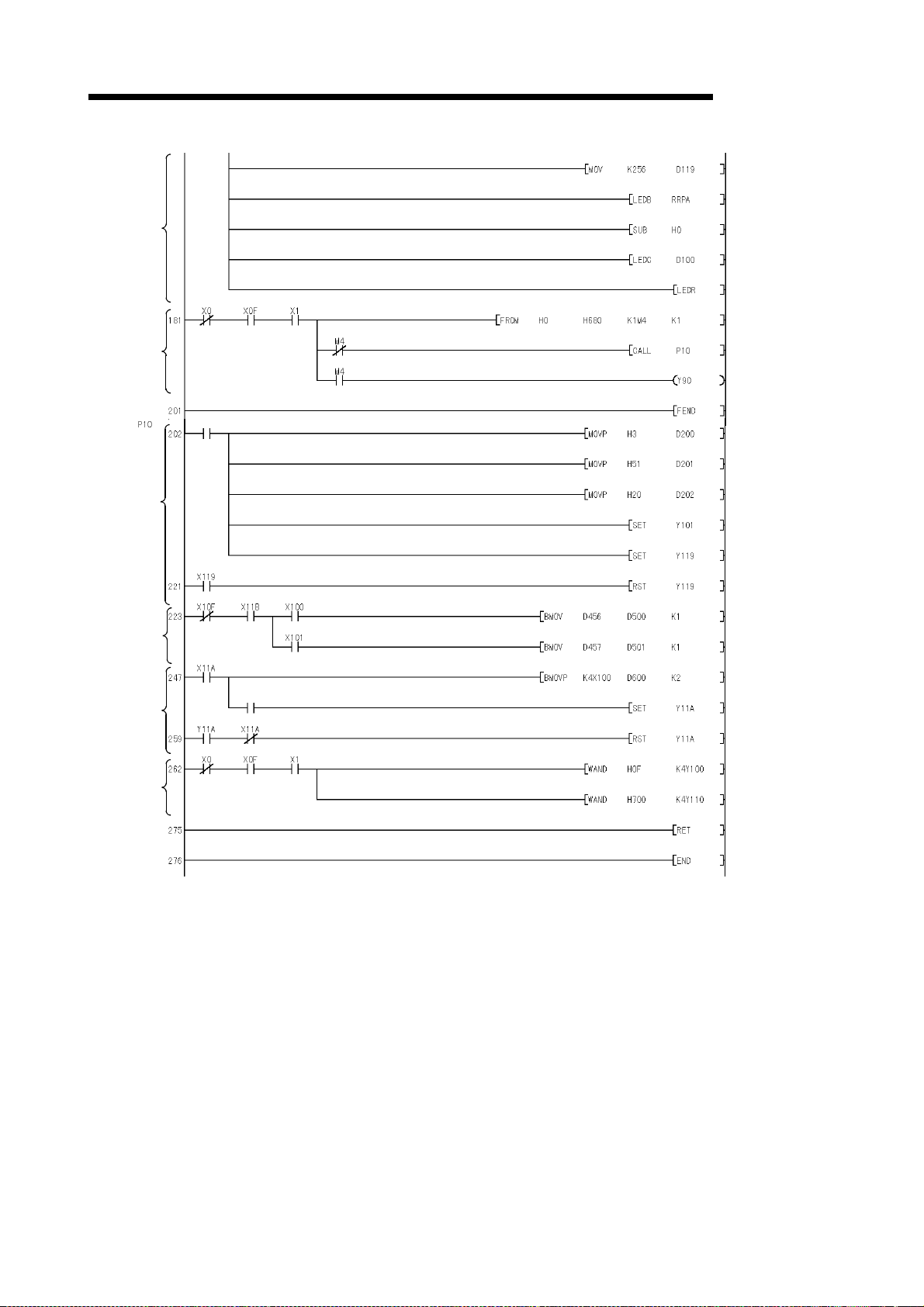
5 PROGRAMMING
Setting of
automatic
refresh
parameters
Checking
of AJ65SBT
-64AD status
MELSEC-A
Sets 256 points.
Dedicated instruction
(RRPA)
Starting I/O number of
master module
Parameter storage
starting device
Reads data link status.
AJ65SBT-64AD data
link normal
AJ65SBT-64AD data
Error LED
link abnormal
Initial
settings
Read of
digital values
Processing
at error
occurrence
Masks
disabled
devices.
User designation
User designation
CH.1, CH.2: A/D
conversion enabled
CH.1: 0 to 5V
CH.2: User range
setting 1
CH.2 moving ave rage
processing count:
16 times
Turns on CH.2 moving
average processing
specifying flag.
Turns on initial data
setting request flag.
Turns off initial data
setting request flag.
Reads CH.1 digital
value.
Reads CH.2 digital
value.
Reads error.
Turns on error reset
request flag.
Turns off error reset
request flag.
Masks RY100 to
RY10F disabled
devices.
Masks RY110 to
RY11F disabled
devices.
5 - 11
Page 53

5 PROGRAMMING
5.2.3 Program examples for use of the QnAC PU
The program examples in this section are created under the following conditions.
GPPW is used to set the network and automatic refresh parameters.
[Relationships between PLC CPU, master module and AJ65SBT-64AD]
PLC CPU
Device X
X100 to X10F
X110 to X11F
Device Y
Y100 to Y10F
Y110 to Y11F
Address
Master module
Remote input (RX)
H
E0
H
E1
Remote output (RY)
H
160
H
161
RX00 to RX0F
RX10 to RX1F
RY00 to RY0F
RY10 to RY1F
MELSEC-A
AJ65SBT-64AD
(Station number 1)
Remote input (RX)
RX00 to RX0F
RX10 to RX1F
Remote output (RY)
RY00 to RY0F
RY10 to RY1F
Device D
D200
D201
D202
D203
Device D
D300
D301
D302
D303
Remote register (RWw)
H
1E0
1E1
1E2
1E3
H
H
H
RWw0
RWw1
RWw2
RWw3
Remote register (RWr)
H
2E0
H
2E1
H
2E2
H
2E3
RWr0
RWr1
RWr2
RWr3
Remote register (RWw)
RWw (A/D conversion
enable/prohibit specification)
RWw1 (Input range setting)
RWw2 (Moving average processing
count setting)
RWw3 (Reserved)
Remote register (RWr)
RWr (CH.1 digital output value)
RWr1 (CH.2 digital output value)
RWr2 (CH.3 digital output value)
RWr3 (CH.4 digital output value)
[Initial settings]
A/D conversion enabled channels.................Channels 1, 2
Moving average processing channel.............Channel 2 count setting = 16 times
Input range setting .........................................Channel 1: 0 to 5V
Channel 2: User range setting 1
[Network parameter setting]
5 - 12
Page 54
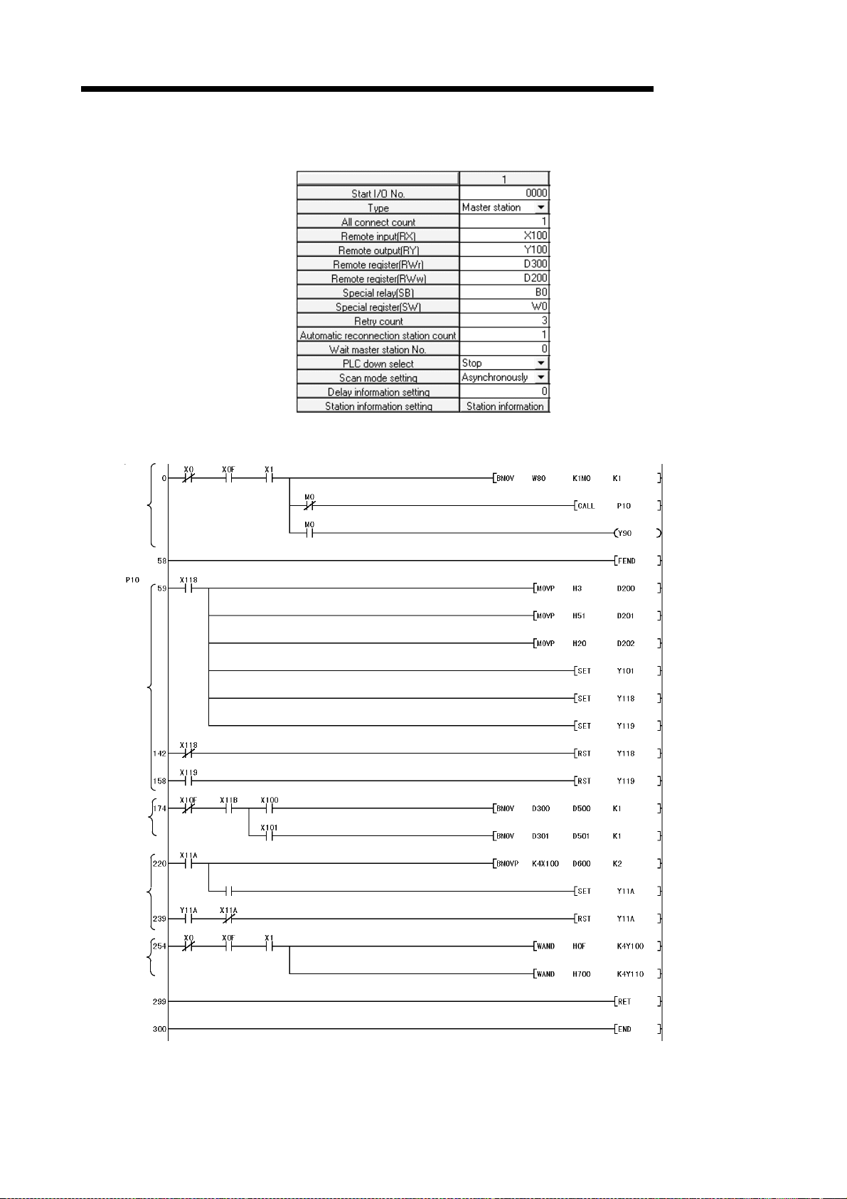
5 PROGRAMMING
MELSEC-A
[Automatic refresh parameter setting]
(1) Program example for pow er - on
Checking
of AJ65SBT
-64AD status
Initial
settings
Read of
digital values
Processing
at error
occurrence
Masks
disabled
devices.
User designation
Error LED
Reads data link status.
AJ65SBT-64AD data
link normal
AJ65SBT-64AD data
link abnormal
CH.1, CH.2: A/D
conversion enabled
CH.1: 0 to 5V
CH.2: User range
setting 1
CH.2 moving average
processing count:
16 times
Turns on CH.2 moving
average processing
specifying flag.
Turns on initial data
processing completion
flag.
Turns on initial data
setting request flag.
Turns off initial data
processing completion
flag.
Turns off initial data
setting request flag.
Reads CH.1 digital
value.
Reads CH.2 digital
value.
Reads error.
Turns on error reset
request flag.
Turns off error reset
request flag.
Masks RY100 to
RY10F disabled
devices.
Masks RY110 to
RY11F disabled
devices.
5 - 13
Page 55
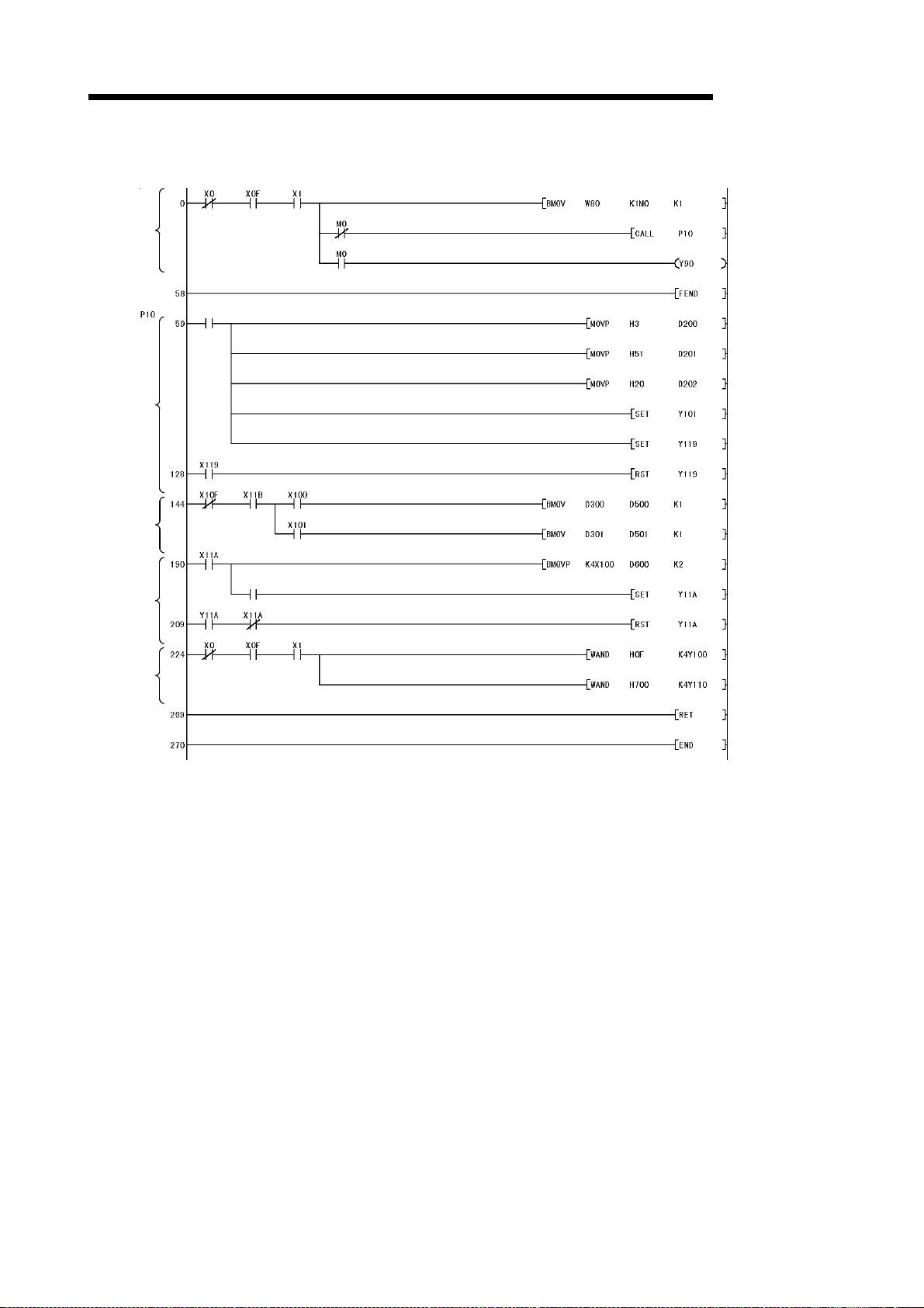
5 PROGRAMMING
MELSEC-A
(2) Program example for init ial data chang i ng
Checking
of AJ65SBT
-64AD status
Initial
settings
Read of
digital values
Processing
at error
occurrence
Masks
disabled
devices.
User designation
User designation
Error LED
Reads data link status.
AJ65SBT-64AD data
link normal
AJ65SBT-64AD data
link abnormal
CH.1, CH.2: A/D
conversion enabled
CH.1: 0 to 5V
CH.2: User range
setting 1
CH.2 moving average
processing count:
16 times
Turns on CH.2 moving
average processing
specifying flag.
Turns on initial data
setting request flag.
Turns off initial data
setting request flag.
Reads CH.1 digital
value.
Reads CH.2 digital
value.
Reads error.
Turns on error reset
request flag.
Turns off error reset
request flag.
Masks RY100 to
RY10F disabled
devices.
Masks RY110 to
RY11F disabled
devices.
5 - 14
Page 56
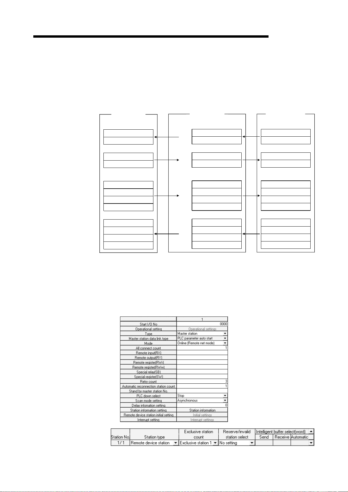
5 PROGRAMMING
5.2.4 Program examples for use of the QC PU ( Q mode)
The program examples in this section are created under the following conditions.
GPPW is used to set the network and automatic refresh parameters.
[Relationships between PLC CPU, master module and AJ65SBT-64AD]
PLC CPU
Device X
X100 to X10F
X110 to X11F
Device Y
Y100 to Y10F
Y110 to Y11F
Address
Master module
Remote input (RX)
H
E0
H
E1
Remote output (RY)
H
160
H
161
RX00 to RX0F
RX10 to RX1F
RY00 to RY0F
RY10 to RY1F
MELSEC-A
AJ65SBT-64AD
(Station number 1)
Remote input (RX)
RX00 to RX0F
RX10 to RX1F
Remote output (RY)
RY00 to RY0F
RY10 to RY1F
Device D
D200
D201
D202
D203
Device D
D300
D301
D302
D303
Remote register (RWw)
H
1E0
1E1
1E2
1E3
H
H
H
RWw0
RWw1
RWw2
RWw3
Remote register (RWr)
H
2E0
H
2E1
H
2E2
H
2E3
RWr0
RWr1
RWr2
RWr3
Remote register (RWw)
RWw (A/D conversion
enable/prohibit specification)
RWw1 (Input range setting)
RWw2 (Moving average processing
count setting)
RWw3 (Reserved)
Remote register (RWr)
RWr (CH.1 digital output value)
RWr1 (CH.2 digital output value)
RWr2 (CH.3 digital output value)
RWr3 (CH.4 digital output value)
[Initial settings]
A/D conversion enabled channels.................Channels 1, 2
Moving average processing channel.............Channel 2 count setting = 16 times
Input range setting .........................................Channel 1: 0 to 5V
Channel 2: User range setting 1
[Network parameter setting]
5 - 15
Page 57
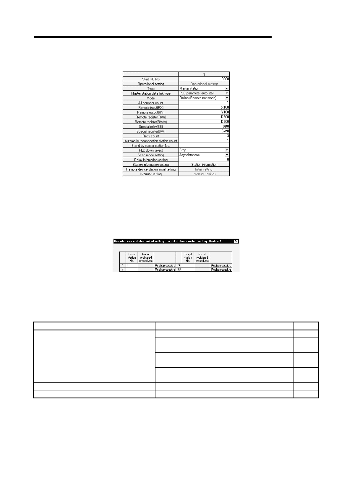
5 PROGRAMMING
MELSEC-A
[Automatic refresh parameter setting]
(1) Program for power-on
At power-on, the initial setting of the AJ65SBT-64AD can be made easily using
the remote device station initialization procedure registration function.
(a) Setting the target station number
Set the station number to which initial setting will be made.
Set the target station number to "1".
(b) Setting the procedure registration
When the initial data processing request flag (RX(n+1)8) turns on and the
remote device station initialization procedure registration (SB0D) is set, the
following data are registered to the AJ65SBT-64AD.
Procedure Execution Condition Execution Number
Channels 1, 2 are set to A/D conversion enable. 1)
Input range setting of channel 1 is set to 0 to 5V.
Input range setting of channel 2 is set to user range setting 1.
Initial data processing request flag (RX(n+1)8) turns on
Initial data processing request flag (RX(n+1)8) turns off Initial data processing completion flag (RY(n+1)8) is turned off. 7)
Initial data setting completion flag (RX(n+1)9) turns on Initial data setting request flag (RY(n+1)9) is turned off. 8)
Moving average processing count of channel 2 is set to 16 times. 3)
Channel 2 is set to moving average processing. 4)
Initial data processing completion flag (RY(n+1)8) is turned on. 5)
Initial data setting request flag (RY(n+1)9) is turned on. 6)
2)
5 - 16
Page 58

5 PROGRAMMING
Checking
of AJ65SBT
-64AD status
(c) Setting results
The setting results of 1) to 8) are shown below.
(d) Program example
MELSEC-A
Reads data link status.
AJ65SBT-64AD data
link normal
AJ65SBT-64AD data
Error LED
link abnormal
Initialization
procedure
registration
Read of
digital values
Processing
at error
occurrence
Masks
disabled
devices.
User designation
Turns on initialization
procedure registration
directive.
Turns off initialization
procedure registration
directive.
Reads CH.1 digital
value.
Reads CH.2 digital
value.
Reads error.
Turns on error reset
request flag.
Turns off error reset
request flag.
Masks RY100 to
RY10F disabled
devices.
Masks RY110 to
RY11F disabled
devices.
5 - 17
Page 59

5 PROGRAMMING
s
MELSEC-A
(2) Program for initial data changi ng
When any initial data (conversion processing system, input range, A/D
conversion ena bl e/di s able chan ne l ) is chan ge d, th e re mote devi ce sta tio n
initialization procedure registration function is unusable.
Using a sequence program, change the initial data.
The program ex a mpl e fo r ini ti al dat a ch anging is shown below .
Checking
of AJ65SBT
-64AD status
Initial
ettings
Read of
digital values
Processing
at error
occurrence
Masks
disabled
devices.
User designation
User designation
Error LED
Reads data link status.
AJ65SBT-64AD data
link normal
AJ65SBT-64AD data
link abnormal
CH.1, CH.2: A/D
conversion enabled
CH.1: 0 to 5V
CH.2: User range
setting 1
CH.2 moving average
processing count:
16 times
Turns on CH.2 moving
average processing
specifying flag.
Turns on initial data
setting request flag.
Turns off initial data
setting request flag.
Reads CH.1 digital
value.
Reads CH.2 digital
value.
Reads error.
Turns on error reset
request flag.
Turns off error reset
request flag.
Masks RY100 to
RY10F disabled
devices.
Masks RY110 to
RY11F disabled
devices.
5 - 18
Page 60

6 TROUBLESHOOTING
6 TROUBLESHOOTING
The details of th e er rors whi c h may occur when usin g t h e AJ65S B T-6 4AD and
troubleshooting are described.
6.1 Using the Remote Input Signals to Check Er ror s
In the AJ65SBT-64AD, occurrence of a write error turns on any of the following remote
input signals.
Device No. Signal Name Description
RXn4 CH.1 range error flag
RXn5 CH.2 range error flag
RXn6 CH.3 range error flag
RXn7 CH.4 range error flag
2
E
RXnC
RX(n+1)A Error status flag
PROM write error flag
Turns on when the value set for input range setting is outside the setting
range.
Turns on if all channels are not set to any of "user range settings 1 to 3" at
offset/gain setting (in the test mode).
Turns on if value write failed due to excess of the E
its limit at the time of offset/gain setting.
If this flag has turned on, this module itself has failed (hardware fault) and
therefore this flag cannot be reset (turned off) by the error reset request flag.
Turns on when CH.
error flag (RXnC) has turned on.
This flag can be reset (turned off) by turning on the error reset request flag.
However, for the E
be reset, either.
range error flag (RXn4 to RXn7) or E2PROM write
2
PROM write error which cannot be reset, this flag cannot
MELSEC-A
2
PROM write count over
6
(1) For the input range setting error (RXn4 to RXn7), the "RUN" LED flickers at
intervals of 0.1 s an d A/ D co nver sio n is not per for med on all chan ne l s .
2
(2) For the E
If the E
PROM write error (RXnC), power on the AJ65SBT-64AD again.
2
PROM write error (RXnC) turns on after power is switched on again, it
indicates a hardware fault. Contact your nearest Mitsubishi representative.
6 - 1
Page 61

6 TROUBLESHOOTING
6.2 Using the LED Indications to Check Error s
This section explains how to check errors using the LED indications of the AJ65SBT64AD.
Refer to the PLC CPU and master module user's manual for issues regarding the PLC
CPU and master module.
(1) When the AJ65SBT-64AD "PW" LED is off
Check item Corrective action
Is 24VDC power on? Check the external power supply.
Is the voltage of the 24VDC power supply within the
specified value?
(2) When the AJ65SBT-64AD "RUN" LED is flashing
Check item Corrective action
Is the LED flickering at 0.1s intervals in the normal
mode?
Is the LED flickering at 0.1s intervals in the test
mode?
Is the LED flickering at 0.5s intervals in the test
mode?
MELSEC-A
Set the voltage value to within the range 20.4 to
26.4V.
1. Using the remote input signals (RXn4 to RXn7),
check the channel at which the input range
setting error has occurred.
2. Make correction to the sequence program or
GPPW setting.
Set all channels to any of "user range settings 1 to
3" in input range setting.
Change the offset/gain adjustment to within the
available setting range.
(3) When the AJ65SBT-64AD "RUN" LED is off
Check item Corrective action
Using the link special registers (SW0084 to
SW0087) of the master module, check the
watchdog timer error and power on the AJ65SBT-
Has the watchdog timer error occurred?
Has the TEST terminals (across 8-9) been shorted
to enter the test mode?
64AD again.
If the "RUN" LED is not lit after power is switched
on again, the possible cause is a hardware fault.
Contact your nearest Mitsubishi representative.
After making offset/gain adjustment, open the TEST
terminals (across 8-9).
(4) When the AJ65SBT-64AD "L RUN" LED is off
Communications are broken.
For details, refer to troubleshooting in the user's manual of the master module
used.
6 - 2
Page 62

6 TROUBLESHOOTING
(5) When the AJ65SBT-64AD "L ERR." LED flickers at fixed intervals
Has the station number or transmission speed
setting switch position been changed during normal
operation?
Is the station number or transmission speed setting
switch faulty?
(6) When the AJ65SBT-64AD "L ERR." LED flickers at unfixed intervals
Have you forgotten fitting the terminal resistor?
Is the module or CC-Link dedicated cable affected
by noise?
MELSEC-A
Check item Corrective action
After correcting the setting sw i tch se tting, switch
power on again.
If the "L ERR." LED has begun flickering though
switch setting change was not made during
operation, the possible cause is a hardware fault.
Contact your nearest Mitsubishi representative.
Check item Corrective action
Check whether the terminal resistor is fitted. If it is
not connected, connect it and switch power on
again.
Earth both ends of the shield wire of the CC-Link
dedicated cable to the protective earth conductor
via SLD and FG of the corresponding module.
Earth the FG terminal of the module without fail.
When carrying out wiring in piping, earth the pipe
without fail.
(7) When the AJ65SBT-64AD "L ERR." LED is on
Check item Corrective action
Are the station number and transmission speed
correct?
Set the correct station number and transmission
speed.
6 - 3
Page 63

6 TROUBLESHOOTING
6.3 When the digital output value cannot be r ead
Check item Corrective action
Is the "PW" LED off? Take action as described in Section 6.2 (1).
Is the "RUN" LED flashing or off? Take action as described in Section 6.2 (2), (3).
Is the "L RUN" LED off? Take action as described in Section 6.2 (4).
Is the "L ERR." LED on?
Is the PLC CPU "RUN" LED flashing or off?
Is the master module "RUN" LED off?
Is the master module [RD] [SD] LED on?
Is the analog input signal line disconnected, cut off,
or any errors?
Remove the AJ65SBT-64AD analog input cable.
Apply the test voltage (stable power supply or
battery) to this module's terminal, and measure the
digital output value.
MELSEC-A
Take action as described in Section 6.2 (7).
Check the error details according to the master
module user's manual.
Check the error details according to the PLC CPU
user's manual.
Check the error details according to the master
module user's manual.
Check the error details according to the master
module user's manual.
Check the error area by checking the signal line
visually or by conductive check.
If he AJ65SBT-64AD module digital output value is
normal, the effects are being received by noise from
an external wiring. So check the wiring and
grounding method.
Lift the AJ65SBT-64AD from the system, and
remove the grounding circuit. (install to the DIN rail.)
6 - 4
Page 64

6 TROUBLESHOOTING
MELSEC-A
6.4 Troubleshooting for the Case where the "ERR ." LED o f the M aster Stati on Fl icker s
The "ERR"LED on the
master station is flashing
Do the parameter
setting and the installed system
configuration match
properly?
Y
Are the master
station link special registers
SW0080 to SW0083 (other station
date link status)
turned on?
Y
Are the master
station link special registers
SW0098 to SW009B (station
number overlap status)
turned on?
Y
Check the module for which
SW0098 to SW009B are on
Are the
station number setting
switches set
properly?
Y
N
Revise the parameter settings
or installed system configuration
N
Master station malfunction
N
N
Set the station number setting
swiches properly
Check the module for which
SW0080 to SW0083 are on
Is the power on?
Y
Check on master station side
Check on slave station side
N
Turn on the power
Corresponding module
malfunction
Turn on the power again
1 2 3
Is the "POWER" LED lit?
Y
6 - 5
N
Is the supplied
power within the specified
range
Y
Corresponding module
malfunction
N
Set the supplied voltage to
within the specified range
Page 65

6 TROUBLESHOOTING
MELSEC-A
1 2 3
Is the "L RUN" LED lit?
Y
N
Are the
station number
setting switches properly
(not overlapping with
other stations)?
Y
Is the transmission speed
setting correct?
Y
Set the correct transmission speed
Is the communication
cable wired properlly ?
*1
Y
N
Set the station number
setting switches properly
N
Turn on the power again
N
Wire the communication
cable properly
Turn on the power again
Corresponding module malfunction
( Transmission speed setting switch )
Are the
station number
setting switches properly
(not overlapping with
other stations)?
Y
Corresponding module malfunction
( station number setting switch )
N
Set the station number
setting switches properly
Turn on the power again
End
*1 Check for a short, reversed connection, wire breakage, terminal resistor, FG connection,
overall distance and station-to-station distance.
6 - 6
Page 66
APPENDIX
APPENDIX
Appendix1 Comparison between This Pr oduct and Conventional Product
(1) Comparison in performance between this product and conventional product
The following table gives performance comparison between the AJ65SBT-64AD
and conventi on al prod u ct ( A J65BT-64AD).
Performance Comparison betw een AJ65SBT-64AD an d C onventional Product
Item
input
Digital outp ut -4096 to +4095 -4000 to +4000
Voltage -10 to +10VDC (input resistance: 1M ) -10 to +10 VDC (input resistance: 1M )Analog
Current 0 to 20mADC (input resistance: 250
AJ65SBT-64AD AJ65BT-64AD
Specifications
) -20 to +20mADC (input resistance: 250 )
MELSEC-A
Input Range
-10 to +10V -10 to +10V 5mV
User range
setting 1
(-10 to +10V)
Voltage
I/O characteristics
Maximum resolution
Current
Input range changing Per channel All channels in batch
Offset/gain setting Yes
Ambient
temperature
Accuracy
Max. conversion speed 1ms/1 channel
Absolute max. input Voltage ±15V, current ±30mA Voltage ±15V, current ±30mA
Number of analog input
points
Number of occupied I/O
points
Connected terminal
block
Applicable wire size
Applicable crimping
terminal
24VDC internal current
consumption (A)
Weight (kg) 0.20 0.35
Outline dimensions
(mm)
0 to 55°C
Ambient
temperature
25±5°C
±0.4% (accuracy relative to maximum value of digital output
±0.2% (accuracy relative to maximum value of digital output
1 station occupied (RX/RY: 32 points each, RWr/RWw: 4
7-point, 2-piece terminal block (transmission, power supply)
Direct-coupled, 18-point terminal block (analog input section)
0 to 5V 1.25mV 0 to 20mA 10µA
1 to 5V 0 to 20mA 5µA
User range
setting 2
(0 to 5V)
0 to 20mA 5µA
4 to 20mA
User range
setting 3
(0 to 20mA)
0.3 to 0.75mm
RAV1.25-3.5 RAV1.25-3.5, RAV2-3.5
118 (W) × 50 (H) × 40 (D) 151.9 (W) × 65 (H) × 63 (D)
Digital
Output
-4000 to
+4000
0 to 4000
0 to 4000
value)
value)
points each)
(M3 screw)
2
0.090 0.12
Max.
Resolution
2.5mV
1.0mV
4µA
4 channels/1 module
Input Range
Voltage
Current
±1.0% (accuracy relative to maximum value of digital output
2 stations occupied (RX/RY: 32 points each, RWr/RWw: 8
0 to 10V 2.5mV
0 to 5V 1.25mV
1 to 5V
-20 to +20mA 20µA
4 to 20mA
points each)
27-point terminal block (M3.5 screw)
0.75 to 2.00mm
Digital
Output
0 to 4000
or -2000
to +2000
0 to 4000
or -2000
to +2000
value)
————
2
Max.
Resolution
1.0mV
4µA
APP
Appendix - 1
Page 67

APPENDIX
MELSEC-A
(2) Precautions for replacing the conv entional pr oduct (AJ65BT-64AD )
with the AJ65SBT-64AD
In the existing system using the conventional product (AJ65BT-64AD), the
following instructions must be noted when changing the AJ65BT-64AD for the
AJ65SBT-64AD.
(a) Since the AJ65SB T-6 4AD occu pie s on e stat io n (t he AJ65B T-6 4 AD occupi e s
two stations), the station information setting in the network parameters must
be changed.
(b) As the remote I/O signals and remote register settings are different between
the two models , the prog ra m of t he con v en ti on al model cannot be utilized .
(c) Because of the differences in shape and layout between the terminal blocks,
you cannot use th e te r mina l bl o c k of t he conv en ti on al modu le as it i s.
(d) The offset/gain setting method differs. For details, refer to Section 4.4.
(e) The ways to set the station number and transmission speed setting switches
are different. For details, refer to Section 4.3.
Appendix - 2
Page 68

APPENDIX
Appendix2 External dimensi on diagr am
The outline dimen si on dr awing of the AJ65SBT-6 4AD is shown below.
MELSEC-A
[4.5]
(0.18)
NP
2-4.5 5.1 installation hole
PW RUN L RUN L ERR. CH1 2 OFFSETGAIN
MITSUBISHI A
DA DG +24V 24G
DB SLD (FG)
4
3
J65SBT-64AD
TEST
TEST
118 (4.65)
109 (4.29) [4.5]
(0.18)
STATION NO. B RATE
40 20 10 8 4 2 1 4 2 1
CH1 CH2
V+ I+
SLD
COM
SELECT
SET
V+ I+
COM
CH3 CH4
V+ I+
COMSLDCOM
V+ I+
ON
AG
(FG1)
40
(1.57)
16.5
(0.65)
504
(1.97)
Appendix - 3
(0.16)
Unit : mm (inch)
Page 69

APPENDIX
MEMO
MELSEC-A
Appendix - 4
Page 70

INDEX
[A]
A/D conversion completion flag.................... 3-11
A/D conversion enable/prohibit
specification................................................. 3-14
Absolute maximum input................................. 3-2
Accuracy....................................................3-2,3-6
Analog input..................................................... 3-2
Analog input points.......................................... 3-2
Applicable master modules............................. 2-2
[C]
CC-Link dedicated cable................................. 4-8
CC-Link dedicated instruction......................... 2-2
Conversion speed ........................................... 3-7
Current input characteristics ........................... 3-5
[D]
Data link cable wiring ...................................... 4-8
Digital output.................................................... 3-2
Digital output value........................................3-16
DIN rail.................................................3-2,4-2,4-4
[E]
E2PROM write error flag ............................... 3-11
Error reset request flag ................................. 3-12
Error status flag............................................. 3-12
External dimension diagram .......................App-3
External power supply..................................... 3-2
[F]
Facing direction of the module installation..... 4-7
Function list...................................................... 3-8
[G]
Gain value........................................................ 3-3
General specification....................................... 3-1
[I]
I/O Conversion Characteristics....................... 3-3
Initial data processing completion flag.......... 3-12
Initial data processing request flag............... 3-11
Initial data setting completion flag................. 3-11
Initial data setting request flag ...................... 3-12
Input range changing function ........................ 3-8
Input range setting......................................... 3-15
Input range setting error ..................................6-1
Internal current consumption...........................3-2
[M]
Maintenance and inspection............................4-9
Maximum resolution.................................. 3-2,3-6
Module connection example............................4-9
Moving average processing ............................3-9
Moving average processing count setting ....3-16
Moving average processing specifying flag..3-12
[N]
Name of each part ...........................................4-3
Number of occupied stations...........................3-2
[O]
Offset value......................................................3-3
Offset/gain adjusting LED................................4-3
Offset/Gain Setting...........................................4-5
Operation status display LED..........................4-3
[P]
Performance comparison between
AJ65SBT-64AD and conventional product
.....................................................................App-1
Performance specification...............................3-2
Pre-Operation procedure.................................4-1
Precaution s fo r re pl a ci ng the conventional
product (AJ65BT-64AD) with the AJ65SBT-64AD
.....................................................................App-2
Precautions when handling .............................4-1
Program examples for use of the
QCPU (Q mode)..........................................5-15
Program examples for use of the QnACPU..5-12
Program examples for use of the ACPU/
QCPU (A mode) (dedicated instructions) .....5-7
Program examples for use of the ACPU/
QCPU (A mode) (FROM/TO instructions) ...5-2
Programming procedure..................................5-1
[R]
Range error flag...................................... 3-11,6-1
Remote I/O signal list.....................................3-10
Remote READY.............................................3-12
Remote register allocation.............................3-13
Resolution ........................................................3-6
Ind
Index - 1
Page 71

[S]
Sampling processing....................................... 3-9
SELECT/SET switch....................................... 4-3
Station number setting switch......................... 4-4
[T]
Terminal block ...........................................3-2,4-4
Terminal number............................................. 4-3
Test mode flag............................................... 3-11
Tightening torque range.................................. 4-2
Troubleshooting............................................... 6-1
Troubleshooting for the case where the
"ERR."LED of the master station flickers ....... 6-5
[U]
User rage setting.......................................3-4,3-5
[V]
Voltage input characteristics........................... 3-4
[W]
Weight.............................................................. 3-2
Wiring............................................................... 4-8
Index - 2
Page 72

MEMO
Index - 3
Page 73

WARRANTY
Please confirm the following product warranty details before starting u se.
1. Gratis Warranty Term and Gratis Warranty Range
If any faults or defects (hereinafter "Failure") found to be the responsibility of Mitsubishi occurs during use of the product
within the gratis warranty term, the product shall be repaired at no cost via the deal er or Mitsubishi Service Company.
Note that if repairs are required at a site overseas, on a detached island or remote place, expenses to dispatch an
engineer shall be charged for.
[Gratis Warranty Term]
The gratis warranty term of the product shall be for one year after the date of purchase or del iv ery to a designat ed
place.
Note that after manufacture and shipment from Mitsubishi, the maximum distribution period shall be six (6) months, and
the longest gratis warranty term after manufacturing shall be eighteen (18) month s. T he gratis w arranty term of repair
parts shall not exceed the gratis warranty term before repairs.
[Gratis Warranty Range]
(1) The range shall be limited to normal use within the usage state, usa ge metho ds and u sage env ironment, etc.,
which follow the conditions and precautions, etc., giv en in the in struction manual, user's manual and caution labels
on the product.
(2) Even within the gratis warranty term, repairs shall be charged for in the follow ing cases.
1. Failure occurring from inappropriate storage or handling, carelessne ss or negl igence by the user. Failure c aused
by the user's hardware or software design.
2. Failure caused by unapproved modifications, etc., to the product by the user.
3. When the Mitsubishi product is assembled into a user' s device, Failure that could hav e been av oided if functions
or structures, judged as necessary in the legal safety measures th e user's dev ice i s subje ct to or as ne ces sary
by industry standards, had been provided.
4. Failure that could have been avoided if consumable parts (battery , backlight, fu se, etc.) de signate d in the
instruction manual had been correctly serviced or replaced.
5. Failure caused by external irresistible forces such as fires or abn ormal v oltages, a nd Failure c aused by force
majeure such as earthquakes, lightning, wind and water damage.
6. Failure caused by reasons unpredictable by scientific technology standards at time of shipment from Mitsubishi.
7. Any other failure found not to be the responsibility of Mitsubishi or the user.
2. Onerous repair term after discontinuation o f producti on
(1) Mitsubishi shall accept onerous product repairs for sev en (7) y ears after production of t he product i s dis continu ed.
Discontinuation of production shall be notified w ith M itsubishi T echnical Bulletins, etc.
(2) Product supply (including repair parts) is not possible after productio n is di scontin ued.
3. Overseas service
Overseas, repairs shall be accepted by M itsubishi' s loc al ov erseas FA Center. N ote that the repair conditio ns at ea ch FA
Center may differ.
4. Exclusion of chance loss and secondary loss from warranty liability
Regardless of the gratis warranty term, Mitsubishi shall not be liable for compensation to damages caused by any cause
found not to be the responsibility of Mitsubishi, chance loss es, lo st profits in curred to the user by Failures of Mitsubishi
products, damages and secondary damages caused fro m spe cial rea sons regardless of Mitsubishi's expectations,
compensation for accidents, and compensation for damages to products other than Mitsubishi products and other duties.
5. Changes in product specifications
The specifications given in the catalogs, manual s or techni cal do cument s are subject to change without prior notice.
6. Product application
(1) In using the Mitsubishi MELSEC programmable logic controller, the usage conditions shall be that the application will
not lead to a major accident even if any problem or fault shoul d occur in the program mable lo gic c ontroller dev ice, and
that backup and fail-safe functions are systematical ly prov ided outside of the dev ice for any proble m or fault.
(2) The Mitsubishi general-purpose programmable logic controll er has been design ed and ma nufactured for a pplications
in general industries, etc. Thus, applications in which the public could be affected such as in nucle ar power plants and
other power plants operated by respective power companies, and applic ations i n which a special quality assurance
system is required, such as for Railway companies or N ational Defen se purpose s sha ll be excluded from the
programmable logic controller applications.
Note that even with these applications, if the user approves that the application is to be limited and a special quality is
not required, application shall be possible.
When considering use in aircraft, medical appli cation s, railw ay s, incineration and fuel dev ices, manned transport
devices, equipment for recreation and amusement, and safety dev ices, i n which human life or assets could be greatly
affected and for which a particularly high reliability is required in term s of safety and c ontrol sy stem, p lease consult
with Mitsubishi and discuss the requ ired spe cificati ons.
Page 74

Analog-Digital Converter Module type AJ65SBT-64AD
User,s Manual
MODEL
MODEL
CODE
AJ65S-64AD-U-S-E
13JR18
SH(NA)-080106-A(0010)MEE
HEAD OFFICE : MITSUBISHI DENKI BLDG MARUNOUCHI TOKYO 100-8310 TELEX : J24532 CABLE MELCO TOKYO
NAGOYA WORKS : 1-14 , YADA-MINAMI 5 , HIGASHI-KU, NAGOYA , JAPAN
When exported from Japan, this manual does not require application to the
Ministry of International Trade and Industry for service transaction permission.
Specifications subject to change without notice.
 Loading...