

Page 1

Technical Information
Operating Instruction
TCR511PEX
Page 2

Contact Information
Meinberg Funkuhren GmbH & Co. KG
Lange Wand 9
D-31812 Bad Pyrmont
Telefon: ++49 (0) 52 81 / 9309-0
Telefax: ++49 (0) 52 81 / 9309-30
Internet: http://www.meinberg.de
Email: info@meinberg.de
September 11, 2007
Page 3

Table of Contents
Contact Information .............................................................................. 2
Diskette with driver software ................................................................ 4
Introduction .......................................................................................... 5
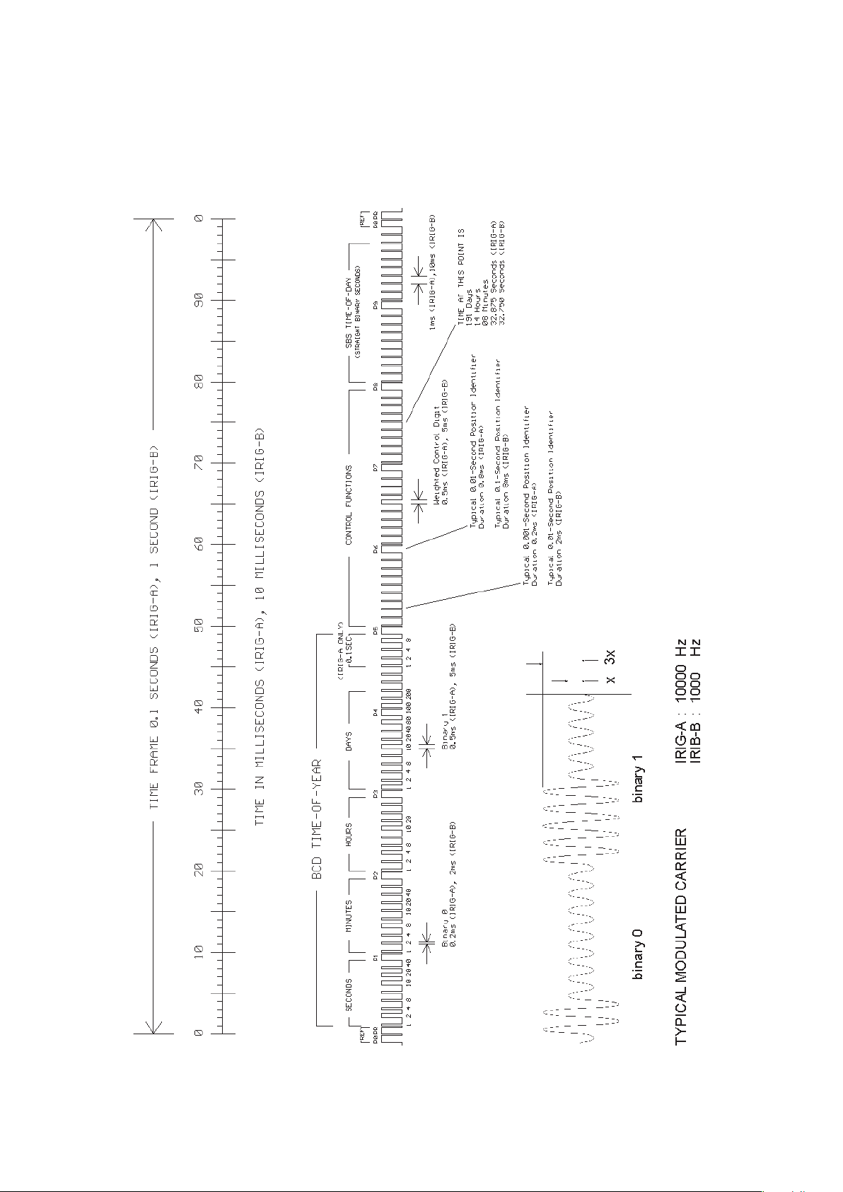
Description of IRIG-Codes................................................................... 5
IRIG-Standard format ........................................................................... 6
AFNOR-Standard format ..................................................................... 7
Features TCR511PEX.......................................................................... 8
Functional description ................................................................. 9
Pulse outputs ............................................................................. 10
Asynchronous serial port........................................................... 10
Connectors and LEDs in the bracket......................................... 10
Pin assignments of the D-Sub-connector................................... 11
Putting into operation.......................................................................... 12
Installing the TCR511PEX in your Computer .......................... 12
Power supply.............................................................................12
Input signals .............................................................................. 12
Input impedance ........................................................................ 13
Photocoupler input .................................................................... 14
Configuration of TCR511PEX ................................................. 14
Firmware Updates .............................................................................. 15
Replacing the Lithium Battery ............................................................ 15
Technical specification TCR511PEX................................................. 16
CE Label ................................................................................... 17
Format of the Meinberg Standard Time String .......................... 18
Page 4

Driver software supplied with the board is keeping the computer’s system time
synchronous to the board time. If the diskette delivered with TCR511PEX doesn’t
include a driver for the used operating system, it can be downloaded free of charge
at:
http://www.meinberg.de/german/sw/
Manuals for the drivers are available at this site also.
The microprocessor system of TCR511PEX is equiped with a Bootstrap-Loader
and a Flash-EPROM. These features enable updating of the onboard software via
the serial RS-232 interface COM0 by using the Meinberg program ‘Flash509’.
4
Page 5

Introduction
The transmission of coded timing signals began to take on widespread importance in
the early 1950´s. Especially the US missile and space programs were the forces behind
the development of these time codes, which were used for the correlation of data. The
definition of time code formats was completely arbitrary and left to the individual ideas of
each design engineer. Hundreds of different time codes were formed, some of which
were standardized by the „Inter Range Instrumantation Group“ (IRIG) in the early 60´s.
Except these „IRIG Time Codes“ other formats, like NASA36, XR3 or 2137, are still
in use. The board TCR511PEX however only decodes IRIG-A, IRIG-B or AFNOR
NFS 87-500 formats. The AFNOR code is a variant of the IRIG-B format. Within this
code the complete date is transmitted instead of the ‘Control Functions’ of the IRIGtelegram.
Description of IRIG-Codes
The specification of individual IRIG time code formats is defined in IRIG Standard 200-
98. They are described by an alphabetical character followed by a three-digit number
sequence. The following identification is taken from the IRIG Standard 200-98 (only the
codes relevant to TCR511PEX are listed):
character bit rate designation A 1000 pps
B 100 pps
1st digit form designation 0 DC Level Shift
width coded
1 sine wave carrier
amplitude modulated
2nd digit carrier resolution 0 no carrier (DC Level Shift)
1 100 Hz, 10 msec resolution
2 1 kHz, 1 msec resolution
3 10 kHz, 100 µsec resolution
3rd digit coded expressions 0 BCD, CF, SBS
1 BCD, CF
2 BCD
3 BCD, SBS
BCD: time of year, BCD-coded
CF: Control-Functions (user defined)
SBS: seconds of day since midnight (binary)
5
Page 6
IRIG-Standard format
6
Page 7

AFNOR-Standard format
7
Page 8

Features TCR511PEX
The board TCR511PEX is designed as a „low profile“ board for computers with PCI
Express interface. The data transfer to the computer is done by using a single PCI
Express Lane (x1 board).
The IRIG receiver is equipped with a standard height bracket. For installation in a „low
profile“ computer, an adequate bracket can be mounted that is included in delivery. The
I/O signals provided by a D-Sub connector are only available when using an additional
bracket (not included) in this case.
TCR511PEX serves to receive and decode modulated (AM) and unmodulated (DC
Level Shift) IRIG and AFNOR time codes. AM-codes are transmitted by modulating the
amplitude of a sine wave carrier, unmodulated codes by variation of the width of pulses.
Automatic gain control within the receive circuit for unmodulated codes allows
decoding of IRIG signals with a carrier amplitude of 600 mVpp to 8 Vpp. The input
stage is elecctically insulated and has an impedance of 50 Ω, it is accessible via the BNC-
connector in the bracket of TCR511PEX
Unmodulated time codes must be connected to the D-Sub-plug of the module. An
onboard photocoupler insulates the internal receive circuit. In delivery state of
TCR511PEX the contacts of the D-Sub-plug are not connected to the photocoupler.
Two DIP-switches must be set to the ‘ON’ position for making this connection.
The board TCR511PEX provides a configurable serial interface (RS-232), a pulse per
second (PPS) with TTL or RS-232 level and a pulse per minute (PPM) with TTL level.
Like the photocoupler, these signals are only connected to the D-Sub-plug after setting
DIP-switches into the ‘ON’ position.
Software running on the computer can read out information regarding date, time and
status of the IRIG receiver. Access to the board is made via writing to/reading from I/O
ports. It is possible but not necessary to let the board generate periodic hardware
interrupts on the computer bus.
8
Page 9

Functional description
After the received IRIG code has passed a consistency check, the software clock and
the battery backed realtime clock of TCR511PEX are synchronized to the external time
reference. If an error in the IRIG telegram is detected, the system clock of the board
switches to holdover mode. Drifting of the internal time base and the generated pulses
(PPS/PPM) is limited to 1µsec/sec by regulating the onboard quartz of TCR511PEX.
IRIG code includes day of year information only. The complete date is kept in the battery
backed realtime clock and the software clock therefore. The received day of year is
compared to this complete date once per minute. If the board detects a difference
between received and stored date information, TCR511PEX switches to holdover mode
but still synchronizes the internal time base to the received IRIG code.
Date and time kept in the realtime clock can be set by sending a Meinberg Standard
Time Telegram to the serial interface COM0 or via the PCI-Express bus.
The internal system clock is always set to the received IRIG time,
which might have a local offset to UTC. Only if TCR511PEX is
configured with this offset, Meinberg driver software is able to set
the system time of the computer correctly. The serial interface COM0
can send the Standard Meinberg Timestring with UTC or local (IRIG)
time.
IRIG telegrams don’t include announcers for the change of time
zone (daylight saving on/off) or for the insertion of a leap second.
Hence the clock will switch into freewheeling mode in case of such
event, and resynchronize afterwards.
The board TCR511PEX decodes the following formats:
A133: 1000pps, amplitude modulated sine wave signal, 10 kHz carrier frequency
BCD time of year, SBS time of day
A132: 1000pps, amplitude modulated sine wave signal, 10 kHz carrier frequency
BCD time of year
A003: 1000pps, DC Level Shift pulse width coded, no carrier
BCD time of year, SBS time of day
A002: 1000pps, DC Level Shift pulse width coded, no carrier
BCD time of year
B123: 100pps, amplitude modulated sine wave signal, 1 kHz carrier frequency
BCD time of year, SBS time of day
B122: 100pps, amplitude modulated sine wave signal, 1 kHz carrier frequency
BCD time of year
B003: 100pps,DC Level Shift pulse width coded, no carrier
BCD time of year, SBS time of day
B002: 100pps, DC Level Shift pulse width coded, no carrier
BCD time of year
AFNOR NFS 87-500:100pps, amplitude modulated sine wave signal, 1 kHz carrier frequency
BCD time of year, complete date, SBS time of day
9
Page 10

Pulse outputs
The module TCR511PEX generates pulses at change of second (PPS) and change of
minute (PPM). The PPS signal is available with TTL (0/+5V) or RS-232 (-3..12V/
+3..12V) level, the PPM signal with TTL level only. If required, DIP-switches can be set
up to direct the pulses to a corresponding pin of the D-Sub-connector in the bracket.
Asynchronous serial port
TCR511PEX provides an asynchronous serial interface (RS-232) called COM0. The
serial port sends a Standard Meinberg Time string either once per second, once per
minute or on request with ASCII ‘?’ only. The format of this telegram is described in the
‘Technical Specifications’. The transmission speed and the framing can be set via the
PCI-Express bus by using the shipped monitor software. Furthermore, the serial
interface COM0 is used for a potential firmware update.
Connectors and LEDs in the bracket
Code
Lock
BSL key
RxD
TxD
GND
antenna
holdov er
The bracket of the board includes the BNCconnector for the amplitude modulated time codes, three LEDs, a key for activating the Bootstrap-Loader and a 9 pin D-Sub-plug.
The LEDs signal the status of the IRIG receiver. The upper, red LED is switched on whenever the internal timing of TCR511PEX is in
holdover mode. This state arises after power up
and if an error in the IRIG telegram is detected.
This LED changes state only at change of
minute.The central, green LED is switched on if
the IRIG receiver detects a correct telegram at its
input. If the below, green LED (Lock) is
switched on, the internal timing of TCR511PEX
is synchronized to the received IRIG code by a
PLL (Phase Locked Loop).
Pressing the hidden key BSL is required for
activating the Bootstrap-Loader before updating
the firmware.
10
Page 11

The 9 pin D-Sub-connector is wired to the board’s serial port. Pin assignment can be
seen from the figure above. This port can not be used as serial port for the computer.
Instead, the clock uses the port to send out Meinberg's standard time string in order to
control an external display or some other external device. The string is sent out once per
second, once per minute or if requested by an incoming ASCII ‘?’. It is also possible to
change the board’s board time by sending such a string towards the clock. Transmission
speed, framing and mode of operation can be modified using the monitor software. The
string format is described in the section ‘Technical Specifications’ at the end of this
manual.
Pin assignments of the D-Sub-connector
Only the signals of the serial interface are connected to the D-Sub-plug directly. If
another signal shall be connected to a pin of the plug, a DIP-switch must be set to the
‘ON’ position.
Whenever an additional signal is connected to the rear panel, special
care must be taken to the configuration of the cable used with the
connector. If pins with TTL level and RS-232 levels are connected to
each other, the circuits on the board may be damaged.
Only one of the switches 5 or 4 may be put in the ‘ON’ position to
connect the pulse per second with TTL level or with RS-232 level to pin 8 of the plug.
The table below shows the pin assignments for the connector and the DIP-switch
assigned to each of the signals:
Pin Signal SWITCH
1+ 5V 3
2 RxD in (RS-232) 3 TxD out (RS-232) 4 PPM out (TTL) 6
5GND 6+ PWM in 1
7- PWM in 2
8 PPS out (TTL/RS232) 5/4
9 (rese rved ) 8
Those signals which do not have DIP-switch assigned are always available at the
connector. All DIP-switches not assigned are reserved and should remain in the ‘OFF’
position.
11
Page 12

Putting into operation
To achieve correct operation of the board, the following points must be observed.
Installing the TCR511PEX in your Computer
Every PCI-Express board is a plug&play board. After power-up, the computer's BIOS
assigns resources like I/O ports and interrupt lines to the board, the user does not need to
take care of the assignments. The programs shipped with the board retrieve the settings
from the BIOS.
The computer has to be turned off and its case must be opened. The board can be
installed in any PCI-Express slot not used yet. The rear plane must be removed before the
board can be plugged in carefully. The computer´s case should be closed again before
restarting the computer.
Power supply
All power supplies needed by TCR511PEX are delivered by the PCI-Express bus.
Input signals
Amplitude modulated IRIG-A/B or AFNOR codes must be connected to the BNC-jack
in the bracket of TCR511PEX. A shielded or a twisted pair cable should be used.
Pulse width modulated (DC Level Shift) signals are applied by using the D-Sub-plug.
Two DIP-switches must be set to the ‘ON’ position for connecting the contacts of the DSub with the onboard photocoupler.
The IRIG code used must be configured with the monitor software.
The board TCR511PEX can’t be used to decode amplitude modulated and DC Level Shift signals simultaneously. Depending on the
selected code, only the signal at the BNC-jack or the D-Sub connector is decoded.
12
Page 13

Input impedance
The IRIG-specification doesn’t define values for the output impedance of generators or
the input impedance of receivers. This fact led to incompatibility of some modules,
because the manufacturers could choose the impedances freely. For example: if the
output impedance of the generator is high and the input impedance of the receiver low,
the signal level at the receiver input might be too low for correct decoding. Therefore the
board TCR511PEX contains a jumper to select the impedance (50 Ω, 600 Ω or 5 kΩ) of
the input for modulated codes (BNC) to comply with the requirements of several
systems.
Meinberg IRIG-generators have an output impedance of 50
ΩΩ
Ω, to build a matched
ΩΩ
transmission system when using a coaxial cable. If such a generator is used to synchronize TCR511PEX, the input impedance has to be set to 50 Ω accordingly (default on
delivery).
In addition to the telegram, the AFNOR-code defines the input/output impedances
also. If TCR511PEX is synchronized by this code, an input impedance of 600
Ω Ω
Ω must be
Ω Ω
set.
The setting „5 kΩ“ may be necessary if the generator has a high output impedance (see
specifications of manufacturer). The driver software shows a bar chart for evaluation of
the signal level at the receiver input.
The following detail of the placeplan of TCR511PEX shows the possible jumper
setting with the related input impedance:
No jumper set: 5K Ohm
Jumper in this Position: 50 Ohm
Jumper in this Position: 600 Ohm
13
Page 14

Photocoupler input
Pulse width modulated (DC Level Shift) codes are insulated by an onboard photocoupler. The connection scheme is shown below:
The internal series resistance allows direct connection of input signals with a maximum high level of +12 V (TTL or RS-422 for example). If signals with a higher
amplitude are used, an additional external series resistance must be applied for not
exceeding the limit of the forward current of the input diode (50 mA). The forward
current should not be limited to a value of less than 10 mA to ensure save switching
of the photocoupler.
Configuration of TCR511PEX
The selection of the IRIG code, configuration of the serial interface and a possible offset
of the received IRIG time to UTC must be set up by the monitor software via the PCIExpress bus. In contrast to AFNOR NFS 87-500 the IRIG telegram containes only the
day of year (1...366) instead of a complete date. To ensure correct function of
TCR511PEX, the date stored in the realtime clock of the board must be
set when using IRIG codes therefore. This setting can be done by a
terminal software also.
If the time zone of the received IRIG code is not UTC, the local offset
to UTC must be configured to ensure correct function of the driver
software. If the local time zone is MEZ for example, the board must be set to a local
offset of ‘+60min’ (MEZ = UTC + 1 h).
The serial interface COM0 can be configured to send a time telegram with reference to
UTC or to the received local IRIG time.
14
Page 15

Firmware Updates
Whenever the on-board software must be upgraded or modified, the new firmware can
be downloaded to the internal flash memory via the board's serial port COM0. There is
no need to open the computer case and insert a new EPROM.
If the button behind a hole in the rear slot cover is pressed for approximately 2
seconds, a bootstrap loader is activated and waits for instructions from the serial port
COM0. A loader program shipped together with the file containing the image of the new
firmware sends the new firmware from one of the computer's serial interfaces to the serial
port COM0. The bootstrap loader does not depend on the contents of the flash memory,
so if the update procedure is interrupted, it can easily be repeated.
The contents of the program memory will not be modified until the loader program has
sent the command to erase the flash memory. So if the button has been pressed
accidentally, the system will be ready to operate again after the computer has been turned
off an the on again.
Replacing the Lithium Battery
The life time of the lithium battery on the board is at least 10 years. If the need arises
to replace the battery, the following should be noted:
ATTENTION!
Danger of explosion in case of inadequate replacement
of the lithium battery. Only identical batteries or batte-
ries recommended by the manufacturer must be used for
replacement. The waste battery must be disposed as
proposed by the manufacturer of the battery.
15
Page 16

Technical specification TCR511PEX
RECEIVER INPUT: AM-input (BNC-connector):
insulated by a transformer
impedance settable 50 Ω, 600 Ω, 5 kΩ
input signal: 600 mVpp to 8 Vpp (Mark)
other ranges on request
DC Level Shift input (D-Sub-connector):
insulated by photocoupler
internal series resistance: 220 Ω
maximum forward current: 50 mA
diode vorward voltage: 1.0 V...1.3 V
DECODING: decoding of the following telegrams possible:
IRIG-A133/A132/A003/A002
IRIG-B123/B122/B003/B002
AFNOR NFS 87-500
ACCURACY OF TIME BASE: +/-5 µsec compared to IRIG reference marker
REQUIRED ACCURACY OF
TIME CODE SOURCE: +/- 100ppm
HOLDOVER MODE: automatic switching to crystal time base
accuracy approximately 1E-6 if decoder has been
synchronous for more than 1h
BACKUP-BATTERY: if the power supply fails, an onboard realtime
clock keeps time and date information
important system parameters are stored in the
RAM of the system
lifetime of the Lithium battery at least 10 years
RELIABILITY OF
OPERATION: microprocessor supervisory circuit provides watch
dog timer, power supply monitoring and backupbattery switchover
software watchdog monitors correct program flow
and generates a reset in case of error detection
INITIALIZATION: software and realtime clock can be set by a serial
Meinberg Standard Telegram via COM0 or the
PCI-Express bus
16
Page 17

OUTPUTS: pulse per second (PPS):
TTL- and RS-232 level
positive pulse, pulse duration 200 msec
pulse per minute (PPM):
TTL level
positive pulse, pulse duration 200 msec
SERIAL PORT: configurable RS-232 interface
baudrates: 300 Bd...38400 Bd
framing: 7E2, 8N1, 8N2, 8E1
mode of operation: string per second
string per minute
string on request
time telegram: Meinberg Standard
Telegram
POWER
REQUIREMENT: +3.3 V: 150 mA
+12 V : 45 mA
power supplies provided by PCI Express interface
PHYSICAL
DIMENSION: low profile expansion board
AMBIENT TEMPERATURE: 0 ... 50°C
HUMIDITY: max. 85 %
CE Label
17
Page 18

Format of the Meinberg Standard Time String
The Meinberg Standard Time String is a sequence of 32 ASCII characters starting with
the STX (start-of-text) character and ending with the ETX (end-of-text) character. The
format is:
<STX>D:dd.mm.yy;T:w;U:hh.mm.ss;uvxy<ETX>
The letters printed in italics are replaced by ASCII numbers whereas the other characters
are part of the time string. The groups of characters as defined below:
<STX> Start-Of-Text (ASCII code 02h)
dd.mm.yy the current date:
dd day of month (01..31)
mm month (01..12)
yy year of the century (00..99)
w the day of the week (1..7, 1 = Monday)
hh.mm.ss the current time:
hh hours (00..23)
mm minutes (00..59)
ss seconds (00..59, or 60 while leap second)
uv clock status characters:
u: ‘ #’ clock has not synchronized after reset
‘ ‘ (space, 20h) clock has synchronized after reset
v: different for DCF77 or GPS receivers:
‘*’ DCF77 clock currently runs on XTAL
GPS receiver has not checked its position
‘ ‘ (space, 20h) DCF77 clock is sync'd with transmitter
GPS receiver has determined its position
x time zone indicator:
‘U’ UTC Universal Time Coordinated, formerly GMT
‘ ‘ (space, 20h) local IRIG time
y ‘ ‘ (space, 20h)
<ETX> End-Of-Text (ASCII code 03h)
18
Page 19

19
Page 20

TCR511PEX - E- 250408
 Loading...