

Page 1

TCR511
Incl. Software TCRMON
Page 2

Impressum
Meinberg Funkuhren GmbH & Co. KG
Auf der Landwehr 22
D-31812 Bad Pyrmont
Telefon: +49 (0) 52 81 / 9309-0
Telefax: +49 (0) 52 81 / 9309-30
Internet: http://www.meinberg.de
Email: info@meinberg.de
October, 30 2006
Page 3

Table of contents
Impressum ............................................................................................ 2
Introduction .......................................................................................... 5
Description of IRIG-Codes................................................................... 5
IRIG-Standard format ........................................................................... 6
AFNOR-Standard format ..................................................................... 7
Overview.....................................................................................8
Function principle ................................................................................. 9
Setting into operation .......................................................................... 10
Supply Voltage..........................................................................10
Input Signals..............................................................................10
Input for unmodulated codes ..................................................... 10
Input for modulated codes ......................................................... 10
Input impedance ........................................................................ 11
Pulse and frequency outputs...................................................... 12
TIME_SYN-Output .................................................................. 12
Serial Ports ................................................................................ 12
Status LEDs .............................................................................. 12
Configuration of the board.................................................................. 13
Selecting the IRIG format..........................................................13
Baudrate and framing of the serial ports ............................................. 14
Output mode of the serial ports..................................................15
DCF Simulation.................................................................................. 16
Updating the Firmware ....................................................................... 17
Replacing the Lithium-Battery............................................................ 17
Technical Specifications TCR511 ...................................................... 18
CE-Label................................................................................... 19
Format of the Meinberg Standard Time String .......................... 21
Page 4

Signals at Rear Connector .................................................................. 22
Rear Connector Pin Assignements ............................................ 23
Diskette with Windows Software TCRMON..................................... 25
The program TCRMON..................................................................... 26
Online Help............................................................................... 27
4
Page 5

Introduction
The transmission of coded timing signals began to take on widespread importance in
the early 1950´s. Especially the US missile and space programs were the forces behind
the development of these time codes, which were used for the correlation of data. The
definition of time code formats was completely arbitrary and left to the individual ideas of
each design engineer. Hundreds of different time codes were formed, some of which
were standardized by the „Inter Range Instrumantation Group“ (IRIG) in the early 60´s.
Except these „IRIG Time Codes“ other formats, like NASA36, XR3 or 2137, are still
in use. The board TCR511 however only decodes IRIG-A, IRIG-B or AFNOR NFS
87-500 formats. The AFNOR code is a variant of the IRIG-B format. Within this code
the complete date is transmitted instead of the ‘Control Functions’ of the IRIG-telegram.
Description of IRIG-Codes
The specification of individual IRIG time code formats is defined in IRIG Standard 200-
98. They are described by an alphabetical character followed by a three-digit number
sequence. The following identification is taken from the IRIG Standard 200-98 (only the
codes relevant to TCR511 are listed):
character bit rate designation A 1000 pps
B 100 pps
1st digit form designation 0 DC Level Shift
width coded
1 sine wave carrier
amplitude modulated
2nd digit carrier resolution 0 no carrier (DC Level Shift)
1 100 Hz, 10 msec resolution
2 1 kHz, 1 msec resolution
3 10 kHz, 100 µsec resolution
3rd digit coded expressions 0 BCD, CF, SBS
1 BCD, CF
2 BCD
3 BCD, SBS
BCD: time of year, BCD-coded
CF: Control-Functions (user defined)
SBS: seconds of day since midnight (binary)
5
Page 6
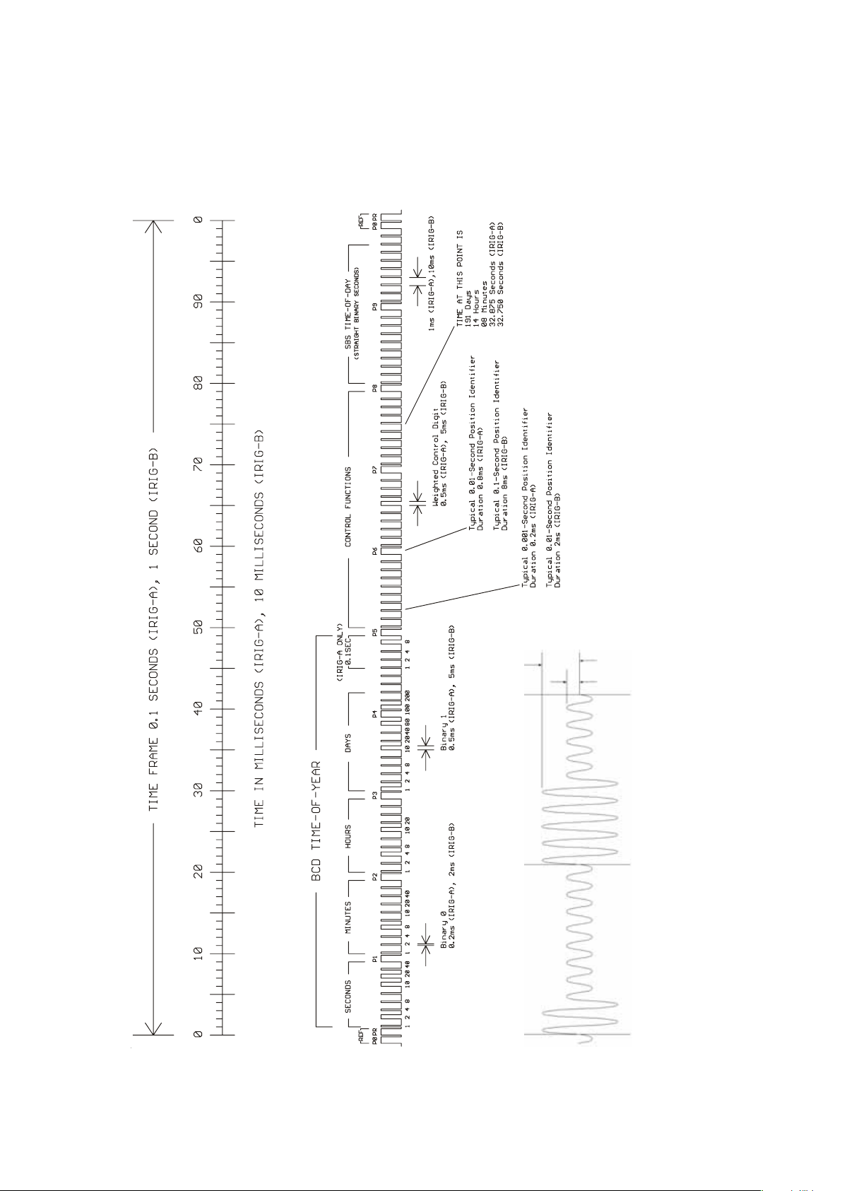
IRIG-Standard format
x 3x
IRIB-B : 1000 Hz
binary 0 binary 1
TYPICAL MODULATED CARRIER IRIG-A : 10000 Hz
6
Page 7
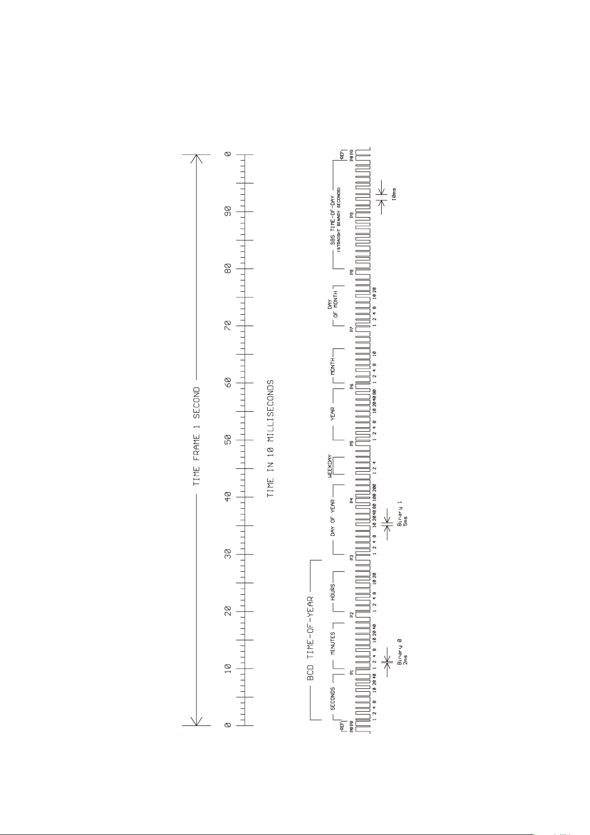
AFNOR-Standard format
7
Page 8

Overview
The Board TCR511 was designed for the decoding of unmodulated and modulated
IRIG- and AFNOR time codes. Modulated codes transport the time information by
modulating a sinusoidal carrier signals amplitude whereas unmodulated signals employ a
pulse width modulated DC signal.
The receivers automatic gain control allows the reception of signals within a range
from abt. 600mVpp up to 8Vpp. The potential free input can be jumper selectable
terminated in either 50Ω, 600Ω or 5kΩ. Modulated codes are applied to the board via an
on board SMB connector.
The unmodulated or 'DC Level Shift' time codes are applied via pins 21c and 22c of
the 64pin VG connector. Galvanic insulation of this input is obtained by an opto coupler
device.
TCR511 provides two configurable serial ports ( RS232 ), a pulse per minute and per
second ( PPS / PPM ) as well as a DCF Simulation port at TTL Level. Further three fixed
frequency outputs at 100kHz, 1MHz and 10MHz at TTL Level are available
The boards micro controller provides a Bootstrap-Loader that allows updating the
firmware stored in Flash-Memory via serial port COM0 by using the program
mbgflash.exe.
8
Page 9
Function principle
After the received IRIG code has passed a consistency check, the software clock and
the battery backed real time clock of TCR511 are synchronized to the external time
reference. If an error in the IRIG telegram is detected, the boards system clock switches
into holdover mode.
Apart from the codes AFNOR NFS 87-500 and IEEE1344, IRIG codes do not carry a
complete date but the number of the day within the current year ( 1...366 ). Hence the
date that is output in the serial telegram must be completed by the date stored in the
buffered real time clock. The day within the current year calculated from the RTCs date
is compared with the day number from the IRIG code every minute. When a mismatch
between these two day numbers is detected the board signalizes freewheeling mode,
however the systems time base will continue to synchronize with the IRIG signal. The
DCF-Simulation is suppressed in this case.
Time and date of the real time clock can be set by a Meinberg Standard Telegram via
serial port COM0. Received IRIG-Time can be re-calculated into UTC provided that no
time zone changeovers such as daylight saving appear in the received IRIG telegrams.
For more information please see chapter 'UTC-Offset' in the online documentation of the
enclosed software TCRMON.
IRIG telegrams don’t include announcers for the change of time
zone (daylight saving on/off) or for the insertion of a leap second.
Hence the clock will switch into freewheeling mode in case of such
event, and resynchronize afterwards.
The board TCR511 decodes the following formats:
A133: 1000pps, amplitude modulated sine wave signal, 10 kHz carrier frequency
BCD time of year, SBS time of day
A132: 1000pps, amplitude modulated sine wave signal, 10 kHz carrier frequency
BCD time of year
A003: 1000pps, DC Level Shift pulse width coded, no carrier
BCD time of year, SBS time of day
A002: 1000pps, DC Level Shift pulse width coded, no carrier
BCD time of year
B123: 100pps, amplitude modulated sine wave signal, 1 kHz carrier frequency
BCD time of year, SBS time of day
B122: 100pps, amplitude modulated sine wave signal, 1 kHz carrier frequency
BCD time of year
B003: 100pps,DC Level Shift pulse width coded, no carrier
BCD time of year, SBS time of day
B002: 100pps, DC Level Shift pulse width coded, no carrier
BCD time of year
AFNOR NFS 87-500:100pps, amplitude modulated sine wave signal, 1 kHz carrier frequency
BCD time of year, complete date, SBS time of day
9
Page 10

Setting into operation
To ensure proper operation, please pay attention to the following points.
Supply Voltage
The boards microprocessor system needs a supply voltage of +5V / 200mA. Additionally the Oscillator supply voltage ( +5V or +12V depends on type ) must be applied via
64pin VG connector. The voltage feed shall be low impendance and for each of the
voltages pins a + c at VG connector shall be used.
Input Signals
Modulated IRIG or AFNOR-Codes are applied via the on board SMB connector. The
lead should be shielded. Unmodulated codes are applied at Pins 21c ad 22c of the 64pin
VG connector. Voltages applied to this input shall not exceed 12V. The IRIG-Code to
be used must be set at the DIP Switch.
Input for unmodulated codes
Unmodulated IRIG-Codes, often referred to as pulse with coded or DC-Level Shift
Codes ( DCLS ), are fed into the board via pins C21 and C22 off the 64pin VG
connector. Insulation of this input is done by a opto coupler device. The input circuitry is
shown below.
Input for modulated codes
Modulated codes must be applied to the on board SMB Connector. An automatic gain
control allows decoding of codes within an amplitude range from abt. 600mVpp up to
8Vpp. To allow adaptation of different time code generators, the boards input impedance
can be selected by an on board jumper.
10
Page 11

Input impedance
The IRIG-specification doesn’t define values for the output impedance of generators or
the input impedance of receivers. This fact led to incompatibility of some modules,
because the manufacturers could choose the impedances freely. For example: if the
output impedance of the generator is high and the input impedance of the receiver low,
the signal level at the receiver input might be too low for correct decoding. Therefore the
board TCR511 provides a jumper to select the impedance (50 Ω, 600 Ω or 5 kΩ) of the
input for modulated codes ( SMB ) to comply with the requirements of several systems.
Meinberg IRIG-generators have an output impedance of 50
ΩΩ
Ω, to build a matched
ΩΩ
transmission system when using a coaxial cable. If such a generator is used to synchronize TCR511, the input impedance has to be set to 50 Ω accordingly (default on delivery).
In addition to the telegram, the AFNOR-code defines the input/output impedances
also. If TCR511 is synchronized by this code, an input impedance 600
Ω Ω
Ω of must be set.
Ω Ω
The setting „5 kΩ“ may be necessary if the generator has a high output impedance (see
specifications of manufacturer). The driver software shows a bar chart for evaluation of
the signal level at the receiver input.
The following detail of the place plan of TCR511 shows the possible jumper setting
with the related input impedance:
JP1 in position 1 - 50
JP1 in position 2 - 600
JP1 open - abt. 5k
11
Page 12

Pulse and frequency outputs
The board provides pulses on second and minute changeover ( P_SEC, P_MIN ).
Additionally fixed frequencies at 100kHz, 1MHz and 10MHz are derived from the
master oscillator. Each of these signals is available at TTL Level on the rear panel 64pin
connector.
TIME_SYN-Output
This TTL output can be used to monitor the synchronization state of the board. The
TIME_SYN signal is in high state whenever the clock is synchronized with the applied
IRIG-Code. It shows low state when the applied code cannot be read, the consistency
check fails or a system failure like brown-out or watchdog reset occurs.
Serial Ports
The board provides two indepentently configurable serial ports at RS232 level. Both
serial ports output the Standard Meinberg telegram. Telegrams can either be output
automatically on second changeover or on request ( ASCII char '?' received ). Serial port
COM0 can additionally be used to communicate with the enclosed monitor software. A
firmware update using mbgflash.exe is done via this channel as well.
Status LEDs
The boards state is signalized by two front panel leds. The red FAIL led indicates the free
wheeling mode. It is activated when the board has switched into freewheling mode, and
turned off when the clock is synchronized. The green LOCK led shows the state of the
internal time. LOCK is turned on when the timebase regulation has settled.
12
Page 13

Configuration of the board
Configuration of the IRIG format to be used as well as the serial ports can be done by an
on board DIP-Switch.
Selecting the IRIG format
The IRIG or AFNOR format to be used can be selected by switches SW1-7 to SW1-10.
Please note that modulated and unmodulated code formats are applied to the board at
separate inputs.
Code SW1-7 SW1-8 SW1-9 SW1-10
B122/B123 Off Off Off Off
A132/A133 On Off Off Off
B002/B003 Off On Off Off
A002/A003 On On Off Off
AFNOR NFS 87-500 Off Off On Off
AFNOR NFS 87-500 ( DC ) On Off On Off
The code AFNOR NFS 87-500 ( DC ) is the unmodulated version of the AFNOR code.
This unmodulated code is not standardized. The standard AFNOR-NFS 87-500 confines to the modulated signal.
13
Page 14

Baudrate and framing of the serial ports
Baudrate and framing can be configured independently for each serial port by two DIPswitches.
SW1-1 Baudrate COM0
off 19200
on 9600
Baudrate of COM0
SW1-2 Framing COM0
off 8N1
on 7E2
Framing of COM0
SW1-4 B audrate COM1
off 19200
on 9600
Baudrate of COM1
SW1-5 Framing COM1
off 8N1
on 7E2
Framing of COM1
14
Page 15

Output mode of the serial ports
Two diffrent modes are configurable for each of the serial ports. Mode 'per second'
causes the port to output a timestring automatically on second changeover. In 'on request'
mode the timestring is output on the next second changeover after a serial char '?' ( ASCII
Code 3Fh ) has been received.
SW1-3 Mode COM0
off on request '?'
on per second
Mode of serial port COM0
SW1-6 Mode COM1
off on request '?'
on per second
Mode of serial port COM1
15
Page 16

DCF Simulation
The DCF_MARK output ( TTL ) produces a time mark signal similar to the signals
transmitted by the german VLF time code transmitter DCF77. Within one minute a
complete time code frame is transmitted. Since there are no timezone and leap second
announcements in the IRIG time code, these announcement flags (daylight saving flag,
leap second flag) are neglected. The generated DCF telegram always contains the time
information which is derived from the IRIG Signal and the system clock. When
receiving a time code telegram containing a leap second ( field sec. is 60 ) the DCF
simulation is turned off for a minute. By this the re-synchronization of all clocks
connected to the simulation outputs is enforced. The issued DCF time code frame
contains a date information which is derived from the system clock. The validity of the
system clock date is ensured by a 'day of year' comparison. In case of an invalid system
clock date the DCF simulation is turned off. System clocks initial date can be set via
COM0. In case of brown out or power failure a lithium battery guarantees the system
clocks operation for at least ten years.
P
8
3
M
4
Year of the Century
Month of Year
Day of Week
Day of Month
0
0
2
0
1
0
8
4
2
1
1
0
50
8
4
2
1
4
2
1
40
0
2
0
1
8
4
2
0
30
1
2
P
20
0
1
Hour
P
8
1
1
4
2
(reserved)
10
R
A
1
Z
1
Z
2
20
A
2
S
1
2
4
8
1
0
2
4
0
Minute
0
M Start of Minute (0.1 s)
R RF Transmission via secondary antenna
A1 Announcement of a change in daylight saving
Z1, Z2 Time zone identification
Z1, Z2 = 0, 1: Daylight saving disabled
Z1, Z2 = 1, 0: Da ylight saving enab led
A2 Announcement of a leap second
S Start of time code information
P1, P2, P3 Even parity bits
16
Page 17

Updating the Firmware
Whenever it is necessarry to upgrade the on-board software, the new firmware can be
downloaded using the serial port COM0.
If the on board boot key is pressed during at power up reset, an internal bootstrap-loader
is activated and waits for instructions from the serial port COM0. A loader program will
be shipped together with the file containing the image of the new firmware. The current
fimware is retained in the flash memory until the download program sends a command to
erase the flash. So if the boot sequence was initiated erroneously, the program memory is
not deleted accidently. The system is ready to go after the next power up.
Replacing the Lithium-Battery
The life time of the lithium battery on the board is at least 10 years. If the need arises to
replace the battery, the following should be noted:
ATTENTION!
Danger of explosion in case of inadequate replacement
of the lithium battery. Only identical batteries or batte-
ries recommended by the manufacturer must be used for
replacement. The waste battery must be disposed as pro-
posed by the manufacturer of the battery.
17
Page 18

Technical Specifications TCR511
RECEIVER INPUT: AM INPUT ( SMB-Connector ) :
insulated by transformer
impedance : 50 Ω, 600 Ω, 5 kΩ
selectable by jumper
input signal : abt.600mVpp to 8V (Mark)
other ranges on request
DC-Level Shift Input ( VG-Connector )
insulated by opto-coupler device
internal series resistor : 330Ω
max. input current: 25mA
diode forward voltage : 1.0V...1.3V
DECODING: decoding of the following codes possible :
IRIG-A133/A132/A003/A002
IRIG-B123/B122/B003/B002
AFNOR NFS 87-500
ACCURACY OF TIME BASE : +/- 10us compared to IRIG reference marker
REQUIRED ACCURACY OF
TIME CODE SOURCE : +/- 100ppm
HOLDOVER MODE: automatic switching to crystal time base,
accuracy : see. accuracy of Oscillator
BACKUP BATTERY : onboard realtime clock keeps time and date
in case of power supply failure. System parameters
are stored in battery buffered ram
lifetime of Lithium battery at least 10 years
RELIABILITY OF
OPERATION: microprocessor supervisory circuit generates reset
in case of brown-out, software watchdog generates
reset in case of improper program execution
INITIALIZATION: initial time and date can be set by standard
meinberg telegram via serial port COM0
PULSE OUTPUTS: pulse per second PPS,
TTL-Level pulse, active high, 200ms pulse width
pulse per minute PPM,
TTL-Level pulse, active high, 200ms pulse width
18
Page 19

FREQUENCY OUTPUTS: 10MHz TTL-Level
1MHz TTL-Level
100kHz TTL-Level
RELATIVE ACCURACY OF
FREQUENCIES COMPARED +/- 1e-8 with TCXO-HQ option
TO IRIG SOURCE: +/- 5e-9 with OCXO-LQ option
STATUS OUTPUT: TIME_SYN, TTL LEVEL,
active high when clock is synchronuos
SERIAL PORTS: two independent RS232 ports
BAUDRATES: 9600Bd, 19200Bd
FRAMINGS: 7E2, 8N1
OUTPUT CYCLE: per second or per minute
SERIAL TELEGRAM: Meinberg Standard Telegram
REAR EDGE CONNECTOR: according to DIN41612, type C 64,
rows a+c ( male )
POWER CONSUMPTION: VCC +5V, abt. 300mA
VDD +5V, abt. 50mA with TCXO-HQ option
max. 500mA OCXO-LQ/MQ
PHYSICAL DIMENSIONS: Eurocard 100mm x 160 mm, 1,5mm Epoxy
AMBIENT TEMPERATURE: 0...50°C
HUMIDITY: max. 85%
CE-Label
This device conforms to the directive 89/336/EWG on the
approximation of the laws of the Member States of the European
Community relating to electromagnetc compatibility .
19
Page 20

20
Page 21

Format of the Meinberg Standard Time String
The Meinberg Standard Time String is a sequence of 32 ASCII characters starting with
the STX (start-of-text) character and ending with the ETX (end-of-text) character. The
format is:
<STX>D:dd.mm.yy;T:w;U:hh.mm.ss;uvxy<ETX>
The letters printed in italics are replaced by ASCII numbers whereas the other characters
are part of the time string. The groups of characters as defined below:
<STX> Start-Of-Text (ASCII code 02h)
dd.mm.yy the current date:
dd day of month (01..31)
mm month (01..12)
yy year of the century (00..99)
w the day of the week (1..7, 1 = Monday)
hh.mm.ss the current time:
hh hours (00..23)
mm minutes (00..59)
ss seconds (00..59, or 60 while leap second)
uv clock status characters (depending on clock type):
u: ‘#’ GPS: clock is running free (without exact synchr.)
PZF: time frame not synchronized
DCF77: clock has not synchronized after reset
‘ ‘ (space, 20h)
GPS: clock is synchronous (base accuracy is reached)
PZF: time frame is synchronized
DCF77: clock has synchronized after reset
v: ‘*’ GPS: receiver has not checked its position
PZF/DCF77: clock currently runs on XTAL
‘ ‘ (space, 20h)
GPS: receiver has determined its position
PZF/DCF77: clock is syncronized with transmitter
x time zone indicator:
‘U’ UTC Universal Time Coordinated, formerly GMT
‘ ‘ MEZ European Standard Time, daylight saving disabled
‘S’ MESZ European Summertime, daylight saving enabled
y anouncement of discontinuity of time, enabled during last hour
before discontinuity comes in effect:
‘! ’ announcement of start or end of daylight saving time
‘A’ announcement of leap second insertion
‘ ‘ (space, 20h) nothing announced
<ETX> End-Of-Text (ASCII code 03h)
21
Page 22

Signals at Rear Connector
Signal Pin Description
VCC in (+5V) 1a+c +5V Voltage Supply
VDD in 3a+c Supply Voltage Oscillator
GND 32a+c Ground
31a+c
19a, 20a, 21a, 22a,
23a, 24a, 25a, 26a,
27a, 28a, 29a, 30a
P_SEC 6c pulse p er second, TTL-Level
P_MIN 8 c pulse per minute, TTL-Level
RESERVE 10c Reserved
DCF_MARK 17c DCF-Simulation, TTL-Level
TIME_SYN 19c Status Output, TTL-Level
10MHz 12a Freq. Output10MHz, TTL-Level
1MHz 11a Freq. Output1MHz, TTL-Level
100kHz 10a Freq. Output 100kHz, TTL-Level
UNMOD_IN+ 21c +Input unmodulated IRIG Code
UNMOD_IN- 22c -Input unmodulated IRIG Code
COM0 RxD 26c COM0 RS-232 Input
COM0 TxD 30c COM0 RS-232 Output
COM1 RxD 29c COM1 RS-232 Input
COM1 TxD 24c COM1 RS-232 Output
22
Page 23

Rear Connector Pin Assignements
ac
1 VCC in (+5V) VCC in (+5V)
2
3 VDD in ( OSC ) VDD in ( OSC )
4/BOOT
5
6P_SEC
7
8P_MIN
9
10 100kHz RESERVE
11 1MHz
12 10MHz
13
14
15
16
17 DCF_MARK
18
19 GND TIME_SYN
20 GND
21 GND UNMOD_IN22 GND UNMOD_IN+
23 GND
24 GND COM1 TxD
25 GND
26 GND COM0 TxD
27 GND
28 GND
29 GND COM1 RxD
30 GND COM0 RxD
31 GND GND
32 GND GND
Conncetor acc. DIN41612, type C 64, rows a + c ( male )
23
Page 24

24
Page 25

Diskette with Windows Software TCRMON
25
Page 26

The program TCRMON
The program TCRMON can be used to program the time offset from UTC and the initial
time of Meinberg IRIG-Receivers. The Software is executable under Win9x/2k/NT. To
install TCRMON just run Setup.exe from the included diskette and follow the instructions of the setup program
To obtain a serial connection from IRIG receiver to PC, serial port COM0 of TCR must
be connected to a free serial port of the PC. The host PCs serial port as well as baudrate
and framing can be selected on tab sheet ‚PC-Comport’. The selected serial parameters
of the PC must match to those of the TCR ( see DIP Switches ). Further, serial mode of
the TCR must be set to STRING_PER_SECOND.
26
Page 27

Online Help
The online help can be started by clicking the menu item 'Help' in menu Help. In every
program tab a direct access to a related help topic can be obtained by pressing F1. The
help language can be selected by clicking the menu items Deutsch/Englisch in the Help
Menu.
27
Page 28

TCR511- E- 301006
 Loading...