

Page 1

Technical Information
Operating Instructions
TCR170PEX
Page 2

Impressum
Meinberg Funkuhren GmbH & Co. KG
Lange Wand 9
D-31812 Bad Pyrmont
Telefon: ++49 (0) 52 81 / 9309-0
Telefax: ++49 (0) 52 81 / 9309-30
Internet: http://www.meinberg.de
Email: info@meinberg.de
October 15, 2009
Page 3

Table of Contents
Impressum............................................................................................ 2
Content of the USB stick ..................................................................... 5
Introduction.......................................................................................... 5
Description of IRIG-Codes .................................................................. 6
IRIG-Standard format .......................................................................... 7
AFNOR-Standard format ..................................................................... 8
PCI Express (PCIe) .............................................................................. 9
Features TCR170PEX ........................................................................ 10
Block diagram TCR170PEX .................................................... 12
Functional description of receiver..................................................... 13
Input signals ............................................................................. 14
Input impedance ....................................................................... 15
Photocoupler input ................................................................... 15
Master oscillator ................................................................................ 16
Functionality of the generator ........................................................... 16
Outputs ..................................................................................... 16
Modulated output ............................................................ 16
Unmodulated outputs ...................................................... 17
Pulse outputs ...................................................................................... 17
Asynchronous serial port ......................................................... 18
Enabling of outputs ............................................................................ 18
Time capture inputs ........................................................................... 19
Connectors and LEDs in the bracket ........................................ 20
Pin assignments of the D-Sub connector ................................. 21
Jumper and contact strips .................................................................. 22
Frequency synthesizer ....................................................................... 23
Page 4

Putting into operation ........................................................................ 23
Installing the TCR170PEX in your Computer ......................... 23
Power supply ............................................................................ 23
Configuration of TCR170PEX ................................................. 24
Firmware Updates .............................................................................. 24
Replacing the Lithium Battery .......................................................... 25
Technical specification TCR170PEX ................................................ 26
Format of the Meinberg Standard Time String ....................... 30
Format of the Capture String ................................................... 31
Format of the time string Uni Erlangen (NTP) ....................... 32
Format of the SAT-Time String ............................................... 34
Konformitätserklärung ............................................................. 35
4
Page 5

Content of the USB stick
The included USB stick contains a driver program that keeps the computer´s system
time synchronous to the received IRIG-time. If the delivered stick doesn’t include a
driver program for the operating system used, it can be downloaded from:
http://www.meinberg.de/english/sw/
On the USB stick there is a file called „readme.txt“, which helps installing the driver
correctly.
Introduction
The transmission of coded timing signals began to take on widespread importance
in the early 1950´s. Especially the US missile and space programs were the forces
behind the development of these time codes, which were used for the correlation of
data. The definition of time code formats was completely arbitrary and left to the
individual ideas of each design engineer. Hundreds of different time codes were
formed, some of which were standardized by the „Inter Range Instrumantation
Group“ (IRIG) in the early 60´s.
Except these „IRIG Time Codes“ other formats, like NASA36, XR3 or 2137, are
still in use. The board TCR170PEX however only decodes IRIG-A, IRIG-B or
AFNOR NFS 87-500 formats. The AFNOR code is a variant of the IRIG-B format.
Within this code the complete date is transmitted instead of the ‘Control Functions’
of the IRIG-telegram.
5
Page 6

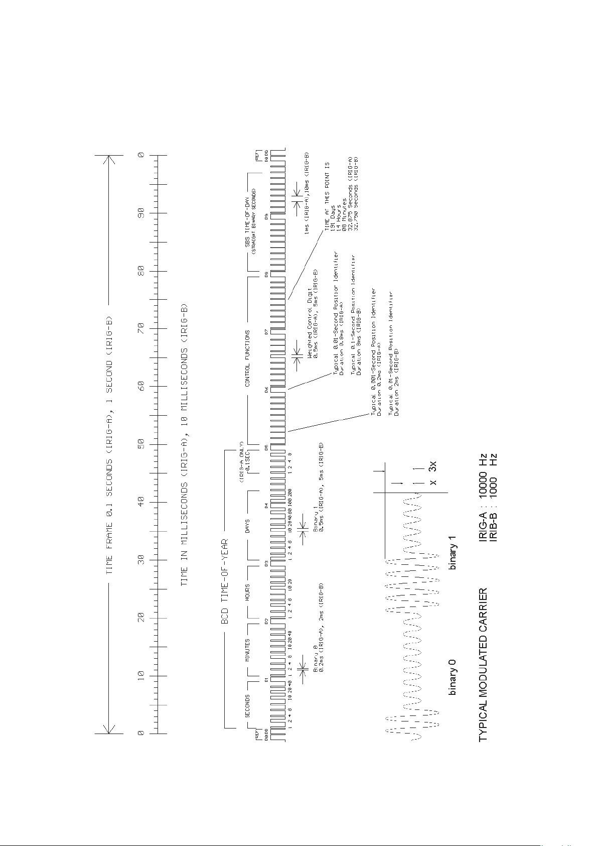
Description of IRIG-Codes
The specification of individual IRIG time code formats is defined in IRIG Standard
200-98. They are described by an alphabetical character followed by a three-digit
number sequence. The following identification is taken from the IRIG Standard 20098 (only the codes relevant to TCR170PEX are listed):
character bit rate designation A 1000 pps
B 100 pps
1st digit form designation 0 DC Level Shift
width coded
1 sine wave carrier
amplitude modulated
2nd digit carrier resolution 0 no carrier (DC Level Shift)
1 100 Hz, 10 msec resolution
2 1 kHz, 1 msec resolution
3 10 kHz, 100 μsec resolution
3rd digit coded expressions 0 BCD, CF, SBS
1 BCD, CF
2 BCD
3 BCD, SBS
BCD: time of year, BCD-coded
CF: Control-Functions (user defined)
SBS: seconds of day since midnight (binary)
6
Page 7
IRIG-Standard format
7
Page 8
AFNOR-Standard format
8
Page 9
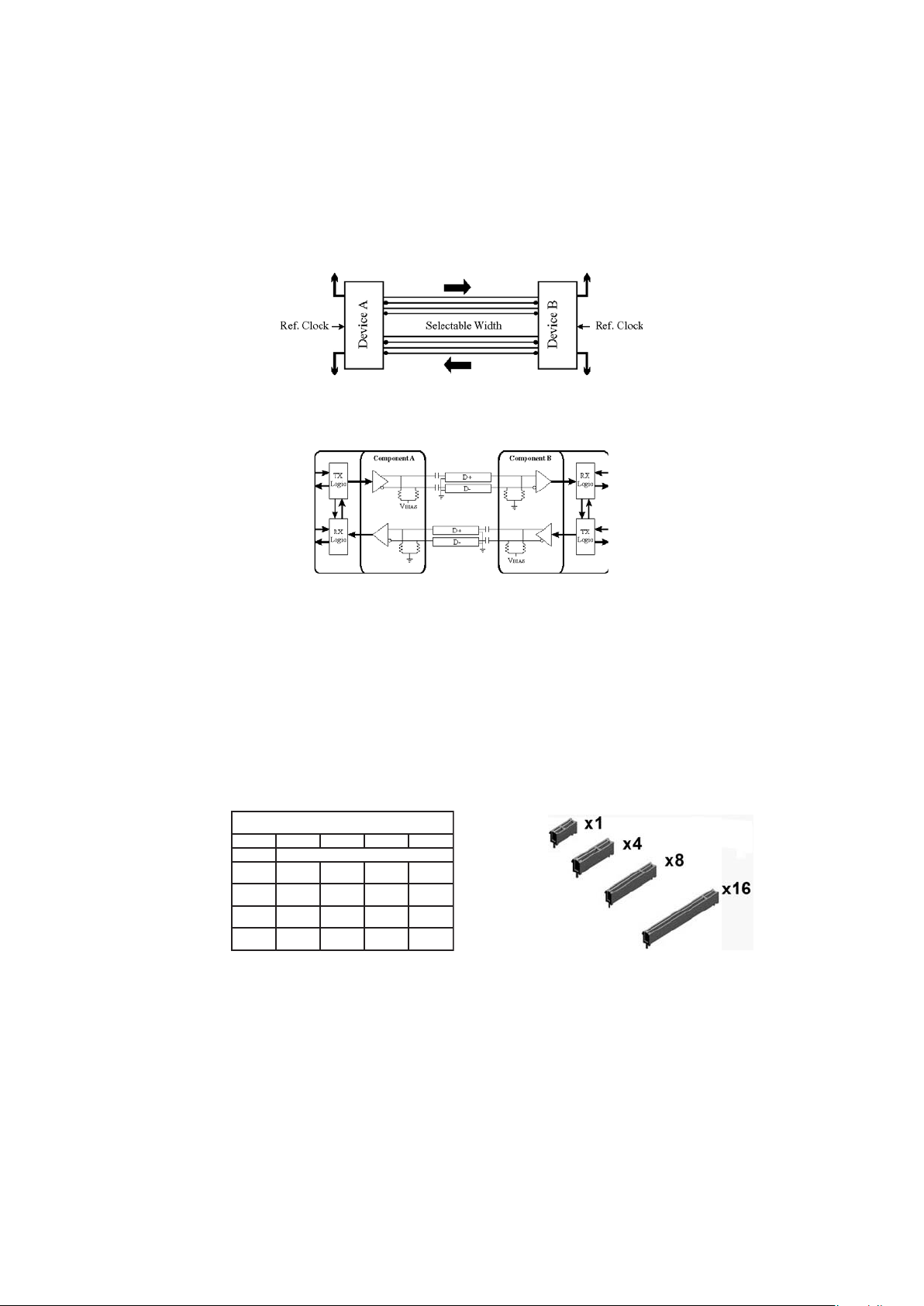
PCI Express (PCIe)
The main technical inovation of PCI Express is a serial data transmission compared
to the parallel interfaces of other computer bus systems like ISA, PCI and PCI-X.
PCI Express defines a serial point-to-point connection, the so-called Link:
The data transfer within a Link is done via Lanes, representing one wire pair for
sending and one wire pair for receiving data:
This design leads to a full duplex connection clocked with 2.5 GHz capable of
transfering a data volume of 250 MB/s per lane in each direction. Higher bandwith is
implemented by using multiple lanes silmutaneously. A PCI Express x16 slot for
example uses sixteen lanes providing a data volume of 4 GB/s. For comparison: when
using conventional PCI the maximum data transfer rate is 133 MB/s, PCI-X allows 1
GB/s but only in one direction respectively. A PCIe expansion board (x1 like
TCR170PEX for example) can always be used in slots with a higher lane width
(x4, x8, x16):
ytilibareporetnIytilibareporetnI
ytilibareporetnIytilibareporetnI
ytilibareporetnI
tolStolS
tolStolS1x1x1x1
x1x4x4x4x4x4x8x8x8x8x8x61x61x
tolS
draCdraC
draCdraC
draC
1x1x1x1x1xseYseY
4x4x4x4x4xoNoNoNoNoNseYseY
8x8x8x8x8xoNoNoNoNoNoNoNoNoNoNseYseY
1x
seYseYseYseY
seYseYseYseY
seY
seY
seYseYseYseY
seY
61x61xoNoNoNoNoNoNoNoNoNoNoNoNoNoNoNseYseY
61x6
61x
seYseYseYseY
seY
seYseYseYseY
seY
seYseYseYseY
seY
61x61x
61x
seYse
Y
seY
seYseY
seY
seYseY
seY
seYseY
seY
One of the strong points of PCI Express is the 100% software compatibility to the
well known PCI bus, leading to a fast spreading. The computer and the operating
system are „seeing“ the more powerfull PCIe bus just as the convetional PCI bus
without any software update.
9
Page 10

Features TCR170PEX
The board TCR170PEX is designed as a standard height board for computers with
PCI Express interface. The data transfer to the computer is done by using a single PCI
Express Lane (x1 board). TCR170PEX serves to decode and generate modulated
(AM) and unmodulated (DC Level Shift) IRIG and AFNOR time codes. AM-codes
are transmitted by modulating the amplitude of a sine wave carrier, unmodulated
codes by variation of the width of pulses.
As standard the module TCR170PEX is equipped with a TCXO (Temperature
Compensated Xtal Oscillator) as master oscillator to provide a high accuracy in
holdover mode of +/- 1 * 10E-8. Optionally an OCXO (Oven Controlled Xtal
Oscillator) is available for better accuracy.
Receiver:
Automatic gain control within the receive circuit for unmodulated codes allows
decoding of IRIG or AFNOR signals with a carrier amplitude of 600 mVpp to 8 Vpp.
The input stage is electrically insulated and has an impedance of either 50 Ω, 600 Ω
or 5 kΩ, selectable by a jumper. The unmodulated input is accessible via a BNCconnector in the bracket of TCR170PEX.
Unmodulated or ‘DC Level Shift’ time codes must be connected to the D-Sub-plug
of the module. The receive circuit is insulated by an onboard photocoupler which can
be driven by TTL or RS-422 signals for example. In delivery state of TCR170PEX the
contacts of the D-Sub-plug are not connected to the photocoupler. Two DIP-switches
must be set to the ‘ON’ position for making this connection.
Generator:
The generator of TCR170PEX is capable of producing time codes in IRIG-B or
AFNOR format. They are available as modulated (3 Vpp/1 Vpp into 50 Ω) and
unmodulated (DC Level Shift) signals (TTL into 50 Ω and RS-422). A jumper on the
board allows selection of active-high or active-low time codes.
Regarding time code and its offset to UTC, the receiver and the generator can be
configured independantly. Thus TCR170PEX can be used for code conversion.
As an option the module can be delivered with optical inputs/outputs instead of the
modulated signal paths.
The board TCR170PEX provides two configurable serial interfaces (RS-232).
COM0 is available via the Sub-D connector, COM1 can be found at a contact strip of
the board. Two programmable pulse outputs can be connected to the D-Sub-plug by
setting DIP-switches into the ‘ON’ position.
A contact strip on the board provides two TTL inputs (CAP0 and CAP1) that can be
used to capture asynchronous time events. These time stamps are readable via the
PCI-bus or the serial interface and can be evaluated by user software.
10
Page 11

TCR170PEX provides a synthesizer which can generate output frequencies from 1/
8 Hz up to 10 MHz with TTL level into 50 Ω and as a sine signal.
11
Page 12

Block diagram TCR170PEX
12
Page 13

Functional description of receiver
After the received IRIG code has passed a consistency check, the software clock
and the battery backed realtime clock of TCR170PEX are synchronized to the
external time reference. If an error in the IRIG telegram is detected, the system clock
of the board switches to holdover mode. IRIG code includes day of year information
only (1...366) and no complete date. The complete date is calculated by using the
IRIG day of year information and the year stored in the battery backed realtime
clock. To achieve synchronization of TCR170PEX, the year stored in the realtime
clock must be set correctly therefore. Date and time kept in the realtime clock can be
set by sending a Meinberg Standard Time Telegram to the serial interface COM0 or
via the PCI bus.
The internal system clock is always set to the received IRIG time,
which might have a local offset to UTC. Only if TCR170PEX is
configured with this offset, Meinberg driver software is able to set
the system time of the computer correctly.
Conversion from UTC to local time including handling of daylight saving year by
year can be done by the board´s microprocessor if the corresponding parameters are
set up with the help of the monitor software.
The time zone is entered as offset of seconds from UTC, e.g. for Germany:
MEZ = UTC + 3600 sec, MESZ = UTC + 7200 sec.
The specific date of beginning and end of daylight saving can be generated
automatically for several years. The receiver calculates the switching times using a
simple scheme, e.g. for Germany:
Beginning of daylight saving is the first sunday after March, 25th at two o’clock => MESZ
End of daylight saving is the first sunday after October, 25th at three o’clock => MEZ
The parameters for time zone and switching to/from daylight saving can be set by
using the included monitor program. If the same values for beginning and end of
daylight saving are entered, no switching of time will be made.
The time code output (IRIG, AFNOR) of TCR170PEX can be generated by
using these time zone settings or UTC as reference. This can be set up with by the
monitor program.
IRIG telegrams don’t include announcers for the change of time
zone (daylight saving on/off) or for the insertion of a leap second.
Hence the clock will switch into freewheeling mode in case of such
event, and resynchronize afterwards.
13
Page 14

The board TCR170PEX decodes the following formats:
A133: 1000pps, amplitude modulated sine wave signal, 10 kHz carrier frequency
BCD time of year, SBS time of day
A132: 1000pps, amplitude modulated sine wave signal, 10 kHz carrier frequency
BCD time of year
A003: 1000pps, DC Level Shift pulse width coded, no carrier
BCD time of year, SBS time of day
A002: 1000pps, DC Level Shift pulse width coded, no carrier
BCD time of year
B123: 100pps, amplitude modulated sine wave signal, 1 kHz carrier frequency
BCD time of year, SBS time of day
B122: 100pps, amplitude modulated sine wave signal, 1 kHz carrier frequency
BCD time of year
B003: 100pps,DC Level Shift pulse width coded, no carrier
BCD time of year, SBS time of day
B002: 100pps, DC Level Shift pulse width coded, no carrier
BCD time of year
AFNOR NFS 87-500: 100pps, amplitude modulated sine wave signal, 1 kHz carrier frequency
BCD time of year, complete date, SBS time of day
Input signals
Amplitude modulated IRIG-A/B or AFNOR codes must be connected to the BNCjack in the bracket of TCR170PEX. A shielded or a twisted pair cable should be used.
Pulse width modulated (DC Level Shift) signals are applied by using the D-Subplug. Two DIP-switches must be set to the ‘ON’ position for connecting the contacts
of the D-Sub with the onboard photocoupler.
As an option, an optical input can be equipped instead of the modulated input. It is
available as ST-connector for GI 50/125µm or GI 62,5/125µm gradient fiber.
The IRIG code used must be configured with the monitor software.
The board TCR170PEX can’t be used to decode amplitude modulated and DC Level Shift signals simultaneously. Depending on the
selected code, only the signal at the BNC-jack, the D-Sub or the
optional optical input connector is decoded.
14
Page 15

Input impedance
The IRIG-specification doesn’t define values for the output impedance of generators
or the input impedance of receivers. This fact led to incompatibility of some modules, because the manufacturers could choose the impedances freely. For example: if
the output impedance of the generator is high and the input impedance of the receiver
low, the signal level at the receiver input might be too low for correct decoding.
Therefore the board TCR170PEX contains a jumper to select the impedance (50 Ω,
600 Ω or 5 kΩ) of the input for modulated codes (BNC) to comply with the
requirements of several systems.
Meinberg IRIG-generators have an output impedance of 50
ched transmission system when using a coaxial cable. If such a generator is used to
synchronize TCR170PEX, the input impedance has to be set to 50 Ω accordingly
(default on delivery).
In addition to the telegram, the AFNOR-code defines the input/output impedances
also. If TCR170PEX is synchronized by this code, an input impedance of 600
be set.
The setting „5 kΩ“ may be necessary if the generator has a high output impedance
(see specifications of manufacturer). The driver software shows a bar chart for
evaluation of the signal level at the receiver input.
ΩΩ
Ω, to build a mat-
ΩΩ
Ω Ω
Ω must
Ω Ω
Photocoupler input
Pulse width modulated (DC Level Shift) codes are insulated by an onboard photocoupler. The connection scheme is shown below:
The internal series resistance allows direct connection of input signals with a
maximum high level of +12 V (TTL or RS-422 for example). If signals with a higher
amplitude are used, an additional external series resistance must be applied for not
exceeding the limit of the forward current of the input diode (50 mA). The forward
current should not be limited to a value of less than 10 mA to ensure save switching
of the photocoupler.
15
Page 16

Master oscillator
As standard, TCR170PEX is equipped with a TCXO (Temperature Compensated
Xtal Oscillator) optionally an OCXO LQ/MQ/HQ (Oven Controlled Xtal Oscillator)
as master oscillator. The internal timing of the module, basis for the software clock,
the pulses and the generated time code, is derived from this oscillator. If the reciver
is synchronized by an incomming time code, the oscillator is adjusted to its nominal
frequency. The current correction factor is stored in a non volatile memory (EEPROM) of the system. Therefore a high accuracy in holdover mode of +/- 1 * 10E-8 is
achieved, if the receiver was synchronous for at least one hour.
The 10 MHz standard frequency is available at a contact strip with TTL level into
50 Ω.
Functionality of the generator
The time code generator of TCR170PEX is based on a DDS (Direct Digital Synthe-
sis) frequency generator, which derives the sine carrier of the modulated code from
the reference clock of the master oscillator. The modulation of carrier amplitude
(modulated codes) or pulse duration (unmodulated, DC level shift codes) is synchronized to the pulse per second (PPS) of the system based on the software clock.
The generated time code is independant from the settings for the
received code. It is possible to generated a different format and
offset from UTC therefore.
Outputs
TCR170PEX provides modulated and unmodulated (DC level shift) outputs. As an
option, an optical output can be equipped instead of the modulated output. It is
available as ST-connector for GI 50/125µm or GI 62,5/125µm gradient fiber.
Modulated output
The amplitude-modulated sine carrier is available a BNC-coaxial-plug connector in
the bracket. The carrier for IRIG-B and AFNOR signals is 1 kHz. The signal amplitude is 3Vpp (MARK) and 1Vpp (SPACE) into 50 Ω. The encoding is made by the
number of MARK-amplitudes during ten carrier waves. The following agreements
are valid:
binary ‘0’ : 2 MARK-amplitudes, 8 SPACE-amplitudes
binary ‘1’ : 5 MARK-amplitudes, 5 SPACE-amplitudes
position-identifier : 8 MARK-amplitudes, 2 SPACE-amplitudes
16
Page 17

Unmodulated outputs
The pulse width modulated DC-signals are coexistent to the modulated output and
are available with TTL level into 50 Ω and as RS-422 signal. After bringing DIPswitches into the ‘ON’ position, these outputs are available at the D-Sub connector.
The active state of the unmodulated outputs can be set up by a jumper on the board
TCR170PEX.
Pulse outputs
The pulse generator of TCR170PEX contains three independent channels (PPO0,
PPO1, PPO2). Two of these TTL outputs can be mapped to pins at the 9-pin connector
at the rear slot cover by using a DIL switch, the third channel is available at a contact
strip. The pulse generator is able to provide a multitude of different pulses, which are
configured with the monitor program. The active state of each channel is invertible,
the pulse duration settable between 10 msec and 10 sec in steps of 10 msec. In the
default mode of operation the pulse outputs are disabled until the receiver has
synchronized after power-up. However, the system can be configured to enable those
outputs immediately after power-up.
The following modes can be configured for each channel independently:
Timer mode: Three on- and off-times per day per channel programmable
Cyclic mode: Generation of periodically repeated pulses.
A cycle time of two seconds would generate a pulse at
0:00:00, 0:00:02, 0:00:04 etc.
DCF77-Simulation
mode: The corresponding output simulates the DCF77 time telegram.
The time marks are representing the local time as configured by the user.
Single Shot Mode: A single pulse of programmable length is generated once a day at a
programmable point of time
Per Sec.
Per Min.
Per Hr. modes: Pulses each second, minute or hour
Status: One of three status messages can be emitted:
‘position OK’: The output is switched on if the receiver was able to
compute its position
‘time sync’: The output is switched on if the internal timing is
synchronous to the GPS-system
‘all sync’: Logical AND of the above status messages.
The output is active if position is calculated AND the
timing is synchronized
Idle-mode: The output is inactive
17
Page 18

The default configuration for the pulse outputs is:
PPO0: Pulse each second (PPS), active HIGH, pulse duration 200 msec
PPO1: Pulse each minute (PPM), active HIGH, pulse duration 200 msec
PPO2: DCF77 Simulation
Asynchronous serial port
TCR170PEX provides two asynchronous serial RS-232 interfaces. COM0 is available at the D-Sub connector, COM1 can be found at a contact strip of the module. The
serial ports are sending a time string in the format ‘Standard Meinberg’, ‘Uni
Erlangen’, or ‘SAT’ either once per second, once per minute or on request with
ASCII ‘?’ only. Furthermore they can be set up to send telegrams containing time
capture events automatically or on request. The format of these telegrams is described in the ‘Technical Specifications’. The transmission speed and the framing can be
set via the PCI-bus by using the shipped monitor software. The serial interface
COM0 is used for a potential firmware update also. The serial interfaces transmit the
time zone set up in the appropriate menu. A potential offset to UTC must be set
correctly.
If a serial interface sends capture events automatically, they can’t
be read via the PCI-bus, because they are deleted from the buffer
memory after transmission.
Enabling of outputs
As standard, the generator, the pulse outputs, the serial interfaces and the frequency
synthesizer are switched off after power up until the receiver is synchronized. By
using the monitor software TCR170PEX can be set up to enable the outputs immediately after reset without synchronization. This setting can be done independant for
the pulses, the serial interface and the synthesizer.
Enabling of the generator is coupled with the pulses, because
generation of time codes is synchronized by the pulse per second
(PPS).
18
Page 19

Time capture inputs
Two time capture inputs (CAP0 and CAP1) are provided at a contact strip of
TCR170PEX to measure asynchronous time events. A falling TTL slope at one of
these inputs lets the microprocessor save the current real time in its capture buffer.
From the buffer, capture events are transmitted via the PCI-bus or the serial interface
COM0. The capture buffer can hold more than 500 events, so either a burst of events
with intervals down to less than 1.5 msec can be recorded or a continuous stream of
events at a lower rate depending on the transmission speed of COM1 can be measured. The format of the output string is ASCII, see the technical specifications at the
end of this document for details. If the capture buffer is full a message „** capture
buffer full“ is transmitted, if the interval between two captures is too short the
warning „** capture overrun“ is being sent.
19
Page 20

Connectors and LEDs in the bracket
modulated
timecode input
code lock/holdover
modulated
timecode output
BSL key
RxD
TxD
GND
The bracket of the board includes the
BNC-connectors for the amplitude
modulated time codes (input/output),
two LEDs, a key for activating the
Bootstrap-Loader and a 9 pin D-Subplug.
The LEDs signal the status of the
IRIG receiver. The right, bicolor LED
is switched to red whenever the internal timing of TCR170PEX is in holdover mode. This state arises after power
up and if an error in the IRIG telegram
is detected. This LED changes state
only at change of minute. This LED is
switched to green (lock) if the internal
timing of TCR170PEX is synchronized
to the received IRIG code by a PLL
(Phase Locked Loop). If the left, green
LED (code) is switched on, the IRIG
receiver detected a correct telegram at
its input.
Pressing the hidden key BSL is required for activating the BootstrapLoader before updating the firmware.
The 9 pin D-Sub-connector is wired to the board’s serial port. Pin assignment can
be seen from the figure above. This port can not be used as serial port for the
computer. Instead, the clock uses the port to send out Meinberg's standard time string
in order to control an external display or some other external device. The string is
sent out once per second, once per minute or if requested by an incoming ASCII ‘?’.
It is also possible to change the board’s board time by sending such a string towards
the clock. Transmission speed, framing and mode of operation can be modified using
the monitor software. The string format is described in the section ‘Technical
Specifications’ at the end of this manual.
20
Page 21

Pin assignments of the D-Sub connector
Only the signals of the serial interface are connected to the D-Sub-plug directly. If
another signal shall be connected to a pin of the plug, a DIP-switch must be set to the
‘ON’ position.
Whenever an additional signal is connected to the rear panel,
special care must be taken to the configuration of the cable used
with the connector. If pins with TTL level and RS-232 levels are
connected to each other, the circuits on the board may be damaged.
Because the pins 1/4/8 of the D-Sub connector could be used for two different
signals, only one of the switches assigned to these pins might be put in the ‘ON’
position. The table below shows the pin assignments for the connector and the DIPswitch assigned to each of the signals:
niPniP
niPniPlangiSlangiS
niP
1V5+ ///// )232-SR(tuo0OPP3///// 4
2)232-
3)232-SR(tuoDxT-
4)LTT(tuo1OPP ///// )224-SR(tuoSLCD-6///// 01
5DNG-
6)relpuocotohp(niSLCD+1
7)relpuocotohp(n
8)LTT(tuo0OPP ///// )224-SR(tuoSLCD+5///// 9
9)LTT(tuoSLCD8
margorp:0OPP
SLCD
langiSlangiSHCTIWSHCTIWS
langiS
SR(niDxR-
iSLCD-2
edocemitdetaludomnu,tfihslevelCD:
HCTIWSHCTIWS
HCTIWS
)SPP(dnocesrepeslup:tluafed,tuptuoeslupelbam
)MPP(etunimrepeslup:tluafed,tuptuoeslupelbammargorp:1OPP
Those signals which do not have DIP-switch assigned are always available at the
connector. All DIP-switches not assigned are reserved and should remain in the
‘OFF’ position.
21
Page 22

Jumper and contact strips
The following diagram shows the possible jumper settings and the assignment of the
contact strips of the board TCR170PEX:
22
Page 23

Frequency synthesizer
The frequency synthesizer is capable to generate output frequencies of 1/8 Hz up to
10 MHz as sine wave signal and with TTL level into 50 Ω. If a frequency smaller than
1 kHz has been selected, the following decimal places lead to real fractions of Hertz:
0.1: 1/8 Hz
0.3: 1/3 Hz
0.6: 1/6 Hz
If a frequency of 0 Hz is selected, the synthesizer is turned off.
The phase position of the output frequency can be set from -360° to +360° with a
resolution of 0.1°. If the phase angle is increased, the signal is more delayed. If the
output frequency is bigger than 10 kHz, the phase angle can’t be set.
Putting into operation
To achieve correct operation of the board, the following points must be observed.
Installing the TCR170PEX in your Computer
Every PCI Express board is a plug&play board. After power-up, the computer's BIOS
assigns resources like I/O ports and interrupt numbers to the board, the user does not
need to take care of the assignments. The programs shipped with the board retrieve
the settings from the BIOS.
The computer has to be turned off and its case must be opened. The radio clock can
be installed in any PCI Express slot not used yet. The rear plane must be removed
before the board can be plugged in carefully. The computer´s case should be closed
again and the antenna can be connected to the coaxial plug at the clock's rear slot
cover. After the computer has been restarted, the monitor software can be run in order
to check the clock's configuration.The computer´s case should be closed after installation.
Power supply
All power supplies needed by TCR170PEX are delivered by the PCI bus.
23
Page 24

Configuration of TCR170PEX
The selection of the IRIG code, configuration of the serial interface and a possible
offset of the received IRIG time to UTC must be set up by the monitor software via
the PCI bus. In contrast to AFNOR NFS 87-500 the IRIG telegram containes only the
day of year (1...366) instead of a complete date. To ensure correct function of
TCR170PEX, the date stored in the realtime clock of the board must be set when
using IRIG codes therefore. This setting can be done by a terminal software also.
If the time zone of the received IRIG code is not UTC, the local
offset to UTC must be configured to ensure correct function of the
driver software. If the local time zone is MEZ for example, the
board must be set to a local offset of ‘+60min’ (MEZ = UTC + 1 h).
The serial interface COM0 can be configured to send a time telegram with reference
to UTC or to the received local IRIG time.
Firmware Updates
Whenever the on-board software must be upgraded or modified, the new firmware
can be downloaded to the internal flash memory via the board's serial port COM0.
There is no need to open the computer case and insert a new EPROM.
If the button behind a hole in the rear slot cover is pressed for approximately 2
seconds, a bootstrap loader is activated and waits for instructions from the serial port
COM0. A loader program shipped together with the file containing the image of the
new firmware sends the new firmware from one of the computer's serial interfaces to
the serial port COM0. The bootstrap loader does not depend on the contents of the
flash memory, so if the update procedure is interrupted, it can easily be repeated.
The contents of the program memory will not be modified until the loader program
has sent the command to erase the flash memory. So if the button has been pressed
accidentally, the system will be ready to operate again after the computer has been
turned off an the on again.
24
Page 25

Replacing the Lithium Battery
The life time of the lithium battery on the board is at least 10 years. If the need arises
to replace the battery, the following should be noted:
ATTENTION!
Danger of explosion in case of inadequate replacement of
the lithium battery. Only identical batteries or batteries
recommended by the manufacturer must be used for re-
placement. The waste battery must be disposed as propo-
sed by the manufacturer of the battery.
25
Page 26

Technical specification TCR170PEX
RECEIVER INPUT: AM-input (BNC-connector):
insulated by a transformer
impedance settable 50 Ω, 600 Ω, 5 kΩ
input signal: 600 mVpp to 8 Vpp (Mark)
other ranges on request
DC Level Shift input (D-Sub-connector):
insulated by photocoupler
internal series resistance: 220 Ω
maximum forward current: 50 mA
diode vorward voltage: 1.0 V...1.3 V
optical input(option):
optcal receive power: min. 3µW
optical connector: ST-connector
for GI 50/125µm
or GI 62,5/125µm
gradient fiber
DECODING: decoding of the following telegrams possible:
IRIG-A133/A132/A003/A002
IRIG-B123/B122/B003/B002
AFNOR NFS 87-500
ACCURACY OF TIME BASE: +/-5 μsec compared to IRIG reference marker
REQUIRED ACCURACY OF
TIME CODE SOURCE: +/- 100ppm
HOLDOVER MODE: automatic switching to crystal time base
accuracy approximately +/- 1 * 10E-8 if decoder
has been synchronous for more than 1h
BACKUP-BATTERY: if the power supply fails, an onboard realtime
clock keeps time and date information
important system parameters are stored in the
RAM of the system
lifetime of the Lithium battery at least 10 years
26
Page 27

GENERATOR OUTPUTS: modulated output:
unbalanced sine carrier, 1 kHz
(MARK), 1Vpp (SPACE) into 50 Ω
3V
pp
unmodulated outputs (DCLS):
TTL into 50 Ω
RS-422
active high or low selectable by jumper
optical output (option):
optical power: typ. 15µW
optical connector: ST-connector
for GI 50/125µm
or GI 62,5/125µm
gradient fiber
PULSE OUTPUTS: three programmable outputs, TTL level
Default settings:
active only ‚if sync‘
PPO0: change of second (PPS)
pulse duration 200 msec
valid on rising edge
PPO1: change of minute (PPM)
pulse duration 200 msec
valid on rising edge
PPO2: DCF77 simulation
SERIAL PORT: configurable RS-232 interface
baudrates: 300 Bd...38400 Bd
framing: 7E2, 8N1, 8N2, 8E1
mode of operation: string per second
string per minute
string on request
time telegram: Meinberg Standard,
Uni Erlangen, SAT,
Capture Telegram
CAPTURE INPUTS: triggered by falling TTL slope
pulse repetition time: 1.5 msec min.
resolution: 800 nsec
output of trigger event via PCI-bus or serial
interface
27
Page 28

MASTER OSCILLATOR: TCXO
(Temperature Compensated Xtal Oscillator)
accuracy compared to IRIG-reference:
sync. and 20 min. of operation: ±5.10
first 20 min. after sync.: ±1.10
accuracy of oscillator:
holdover, 1 day: ±1.10
holdover, 1 year: ±1.10
short term stability:
<= 10 sec, synchronized: ±2.10
<= 10 sec, holdover: ±5.10
temperature dependant drift:
holdover: ±1.10
phase noise:
1 Hz besides carrier: -60 dB/Hz
10 Hz besides carrier: -90 dB/Hz
100 Hz besides carrier: -120 dB/Hz
1 kHzbesides carrier: -130 dB/Hz
-9
-8
-7
-6
-9
-9
-6
Option:
OCXO LQ for higher accuracy in holdover mode
(Specifications look at oscillator options on
Meinberg homepage)
FREQUENCY
SYNTHESIZER: output frequency: 1/8 Hz up to 10 MHz
accuracy: like system accuracy
1/8 Hz to 10 kHz: Phase synchronous to
pulse per second
10 kHz to 10 MHz: deviation of frequency
< 0.0047 Hz
outputs: TTL into 50 Ω
sine wave 1.5 V
rms
,
output impedance 200 Ω
Page 29

RELIABILITY OF
OPERATION: microprocessor supervisory circuit provides
watch dog timer, power supply monitoring and
backup battery switchover
software watchdog monitors correct program
flow and generates a reset in case of error
detection
INITIALIZATION: software and realtime clock can be set by a serial
Meinberg Standard Telegram via COM0 or the
PCI Express Interface
BUS
INTERFACE: Single lane (x1) PCI Express (PCIe) Interface
compatible to PCI Express specifications r1.0a
DATA FORMAT: binary, byte serial
POWER REQUIREMENTS: +3,3V, @ 200 mA
+12V, @ 120 mA
BOARD DIMENSIONS: standard height expansion board
AMBIENT TEMPERATURE: 0 ... 70°C
HUMIDITY: max. 85 %
Page 30

Format of the Meinberg Standard Time String
The Meinberg Standard Time String is a sequence of 32 ASCII characters starting
with the STX (start-of-text) character and ending with the ETX (end-of-text) character. The format is:
<STX>D:dd.mm.yy;T:w;U:hh.mm.ss;uvxy<ETX>
The letters printed in italics are replaced by ASCII numbers whereas the other
characters are part of the time string. The groups of characters as defined below:
<STX> Start-Of-Text (ASCII code 02h)
dd.mm.yy the current date:
dd day of month (01..31)
mm month (01..12)
yy year of the century (00..99)
w the day of the week (1..7, 1 = Monday)
hh.mm.ss the current time:
hh hours (00..23)
mm minutes (00..59)
ss seconds (00..59, or 60 while leap second)
uv clock status characters:
u: ‘#’ clock has not synchronized after reset
‘ ‘ (space, 20h) clock has synchronized after reset
v: different for DCF77 or GPS receivers:
‘*’ DCF77 clock currently runs on XTAL
GPS receiver has not checked its position
‘ ‘ (space, 20h) DCF77 clock is sync'd with transmitter
GPS receiver has determined its position
x time zone indicator:
‘U’ UTC Universal Time Coordinated, formerly GMT
‘ ‘ (space, 20h) local IRIG time
y ‘ ‘ (space, 20h)
<ETX> End-Of-Text (ASCII code 03h)
30
Page 31

Format of the Capture String
The Meinberg GPS167 Capture String is a sequence of 31 ASCII characters terminated by a CR/LF (Carriage Return/Line Feed) combination. The format is:
CHx_tt.mm.jj_hh:mm:ss.fffffff<CR><LF>
The letters printed in italics are replaced by ASCII numbers whereas the other
characters are part of the time string. The groups of characters as defined below:
x 0 or 1 corresponding on the number of the capture input
_ ASCII space 20h
dd.mm.yy the capture date:
dd day of month (01..31)
mm month (01..12)
yy year of the century (00..99)
hh:mm:ss.fffffff the capture time:
hh hours (00..23)
mm minutes (00..59)
ss seconds (00..59, or 60 while leap second)
fffffff fractions of second, 7 digits
<CR> Carriage Return, ASCII code 0Dh
<LF> Line Feed, ASCII code 0Ah
31
Page 32

Format of the time string Uni Erlangen (NTP)
The time string Uni Erlangen (NTP) of a GPS-clock is a sequence of 66 ASCII
characters starting with the STX (start-of-text) character and ending with the ETX
(end-of-text) character. The format is:
<STX>tt.mm.jj; w; hh:mm:ss; voo:oo; acdfg i;bbb.bbbbn lll.lllle hhhhm<ETX>
The letters printed in italics are replaced by ASCII numbers whereas the other
characters are part of the time string. The groups of characters as defined below:
<STX> Start-Of-Text (ASCII code 02h)
dd.mm.yy the current date:
dd day of month (01..31)
mm month (01..12)
yy year of the century (00..99)
w the day of the week (1..7, 1 = Monday)
hh.mm.ss the current time:
hh hours (00..23)
mm minutes (00..59)
ss seconds (00..59, or 60 while leap second)
v sign of the offset of local timezone related to UTC
oo:oo offset of local timezone related to UTC in hours and minutes
ac clock status characters:
a: ‘#’ clock has not synchronized after reset
‘ ‘ (space, 20h) clock has synchronized after reset
c: ‘*’ GPS receiver has not checked its position
‘ ‘ (space, 20h) GPS receiver has determined its position
d time zone indicator:
‘S’ MESZ European Summertime, daylight saving enabled
‘ ‘ MEZ European Standard Time, daylight saving disabled
f anouncement of discontinuity of time, enabled during last hour
before discontinuity comes in effect:
‘!’ announcement of start or end of daylight saving time
‘ ‘ (space, 20h) nothing announced
g anouncement of discontinuity of time, enabled during last hour
before discontinuity comes in effect:
‘A’ announcement of leap second insertion
‘ ‘ (space, 20h) nothing announced
i leap second insertion
32
Page 33

‘L’ leap second is actually inserted
(active only in 60th sec.)
‘ ‘ (space, 20h) no leap second is inserted
bbb.bbbb latitude of receiver position in degrees
leading signs are replaced by a space character (20h)
n latitude, the following characters are possible:
‘N’ north of equator
‘S’ south d. equator
lll.llll longitude of receiver position in degrees
leading signs are replaced by a space character (20h)
e longitude, the following characters are possible:
‘E’ east of Greenwich
‘W’ west of Greenwich
hhhh altitude above sea level in meters
leading signs are replaced by a space character (20h)
<ETX> End-Of-Text (ASCII-Code 03h)
33
Page 34

Format of the SAT-Time String
The SAT-Time String is a sequence of 29 ASCII characters starting with the STX
(start-of-text) character and ending with the ETX (end-of-text) character. The format
is:
<STX>dd.mm.yy/w/hh:mm:ssxxxxuv<ETX>
The letters printed in italics are replaced by ASCII numbers whereas the other
characters are part of the time string. The groups of characters as defined below:
<STX> Start-Of-Text (ASCII code 02h)
dd.mm.yy the current date:
dd day of month (01..31)
mm month (01..12)
yy year of the century (00..99)
w the day of the week (1..7, 1 = Monday)
hh.mm.ss the current time:
hh hours (00..23)
mm minutes (00..59)
ss seconds (00..59, or 60 while leap second)
xxxx time zone indicator:
‘UTC‘ Universal Time Coordinated, formerly GMT
‘MEZ‘ European Standard Time, daylight saving disabled
‘MESZ’ European Summertime, daylight saving enabled
u clock status characters:
‘#’ clock has not synchronized after reset
‘ ‘ (space, 20h) clock has synchronized after reset
v anouncement of discontinuity of time, enabled during last hour
before discontinuity comes in effect:
‘!’ announcement of start or end of daylight saving time
‘ ‘ (space, 20h) nothing announced
<CR> Carriage-return (ASCII code 0Dh)
<LF> Line-feed (ASCII code 0Ah)
<ETX> End-Of-Text (ASCII code 03h)
34
Page 35

Konformitätserklärung
Declaration of Conformity
Hersteller Meinberg Funkuhren GmbH & Co. KG
Manufacturer Auf der Landwehr 22
D-31812 Bad Pyrmont
erklärt in alleiniger Verantwortung, daß das Produkt
declares under its sole responsibility, that the product
Produktbezeichnung Time code receiver/generator
Product Name
Modell / Typ TCR170PEX
Model Designation
auf das sich diese Erklärung bezieht, mit den folgenden Normen übereinstimmt
to which this declaration relates is in conformity with the following standards
EN55022, 11/01, Class B Grenzwerte und Meßverfahren für Funkstörun-
gen von informationstechnischen Einrichtungen
Limits and methods of measurement of radio interference
characteristics of information technology equipment
EN55024, 5/99 Grenzwerte und Meßverfahren für Störfestigkeit
von informationstechnischen Einrichtungen
Limits and methods of measurement of Immunity characteristics of information technology equipment
gemäß den Bestimmungen der Richtlinie 89/336/EWG zur Angleichung der Rechtsvorschriften der Mitgliedstaaten über die elektromagnetische Verträglichkeit.
following the provisions of Directive 89/336/EEC on the approximation of the laws of the Member States
relating to electromagnetic compatibility.
Bad Pyrmont, den 04.11.2008
35
Page 36

TCR170PEX- E- 15. 10. 09
 Loading...