

Page 1
Technical Information
Operating Instructions
GEN170TGP
Page 2

Impressum
Meinberg Funkuhren GmbH & Co. KG
Lange Wand 9
D-31812 Bad Pyrmont
Telefon: +49 (0) 52 81 / 9309-0
Telefax: +49 (0) 52 81 / 9309-30
Internet: http://www.meinberg.de
Email: info@meinberg.de
17. November, 2008
Page 3

Index
Impressum ............................................................................................ 2
The Modular System GEN170TGP ..................................................... 5
General Information about DCF77 ....................................................... 6
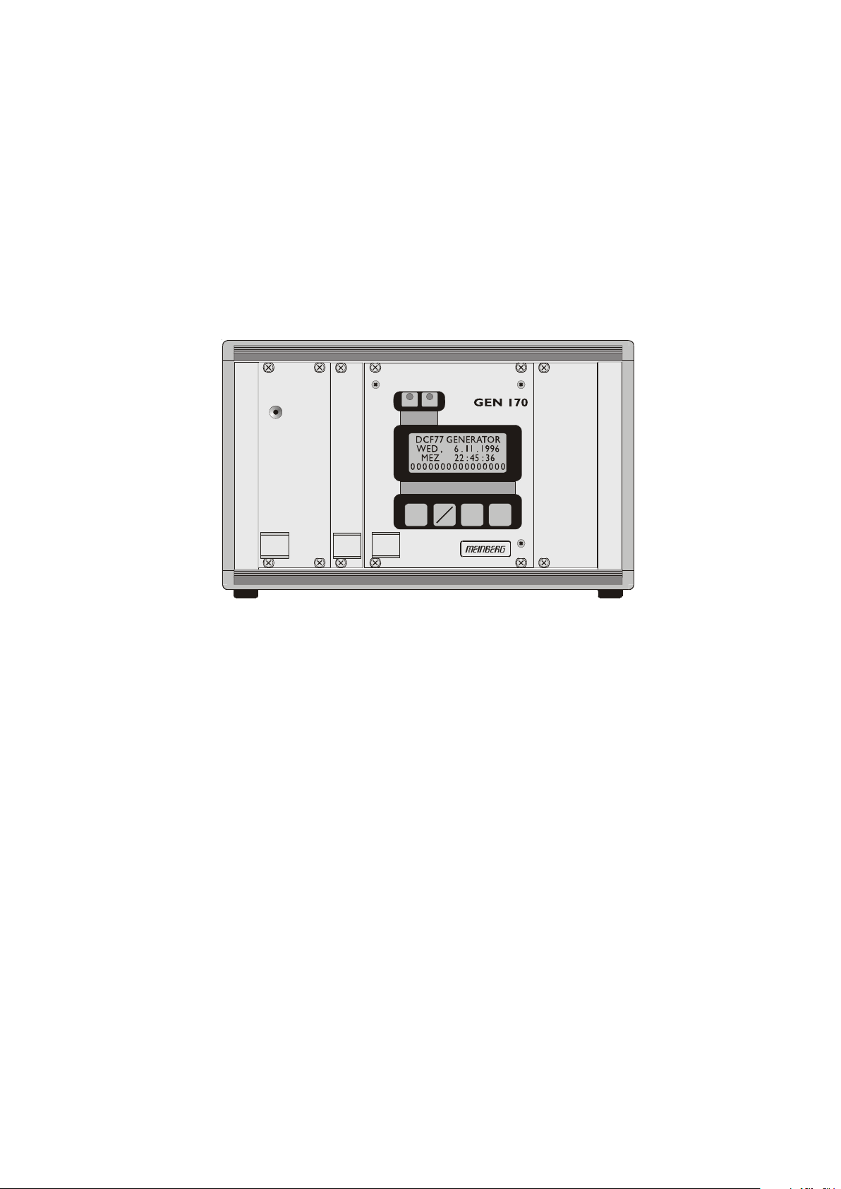
GEN170 ............................................................................................... 7
GEN170 Overview ..................................................................... 7
The GEN170 Front Panel Layout ........................................................ 8
FAIL LED and LOCK LED ...................................................... 8
LC Display .................................................................................. 8
MENU Key................................................................................. 8
CLR/ACK Key ........................................................................... 8
NEXT Key.................................................................................. 8
INC Key...................................................................................... 8
The Menus in Detail ............................................................................. 9
Root Menu .................................................................................. 9
Menu SETUP ..................................................................................... 10
SETUP INITIAL TIME ........................................................... 10
ADJUST SECONDS ............................................................... 10
SETUP TIME ZONE ............................................................... 11
SETUP DAYLIGHT SAV ON/OFF ....................................... 11
SETUP LEAP SECOND ......................................................... 11
SETUP SERIAL PORT PARM............................................... 12
SETUP SER. STRING TYPE ................................................. 12
SETUP SERIAL OUTPUT ..................................................... 13
SETUP TIMECODE OUT ...................................................... 13
INIT USER PARMS ................................................................ 14
Resetting Factory Defaults ........................................................ 14
Firmware Updates ..................................................................... 14
Page 4

Format of the Meinberg Standard Time String .......................... 15
Time code ........................................................................................... 16
Principle of Operation ............................................................... 16
Block Diagram Time code ........................................................ 16
IRIG Standard Format ............................................................... 17
AFNOR Standard Format ......................................................... 18
Assignment of CF Segment in IEEE1344 mode ....................... 19
Generated Time codes ............................................................... 20
Selection of Generated Time Code .................................. 21
Outputs ............................................................................ 21
AM Sine Wave Output .................................................... 21
PWM DC Output............................................................. 21
Technical Data ................................................................. 21
Technical Specifications GEN170 ..................................................... 22
Signal Description GEN170 .............................................................. 24
Rear Connector Pin Assignments GEN170 ........................................ 25
DCF77-Simulator ............................................................................... 26
Function .................................................................................... 26
Technical Specifications SIM77PV4......................................... 27
Rear Connector Pin Assignments SIM77PV4........................... 28
GEN170TGP Rear view ........................................................... 29
Assignments of the 25 pin Connector........................................ 29
4
Page 5
The Modular System GEN170TGP
GEN170TGP is a set of equipment composed of a DCF77 generator GEN170 and a
DCF77 simulator SIM77PV4 together with a power supply, all installed in a metal
desktop case and ready to operate. The interfaces and signals provided by GEN170 and
SIM77PV4 are accessible via connectors in the rear panel of the case. Details of the
components are described below.
FAIL LOCK
CLR
ACK
NEXT INC
MENU
GEN170 assembled in desktop case
5
Page 6
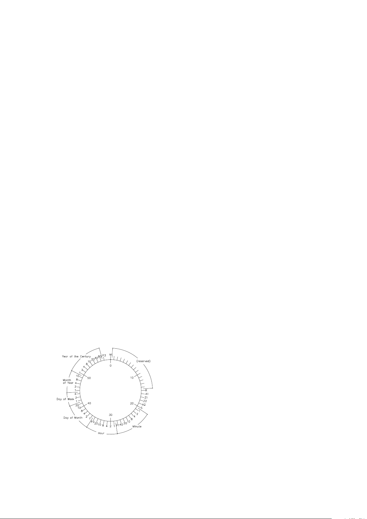
General Information about DCF77
The long wave transmitter DCF77 is installed in Mainflingen near Frankfurt/Germany
and transmits the reference time of the Federal Republic of Germany. This is either the
Central European Time (Mitteleuropäische Zeit, MEZ) or the Central European Summer
Time (Mitteleuropäische Sommerzeit, MESZ). The transmitter is controlled by the
atomic clock plant at the Federal Physical Technical Institute (PTB) in Braunschweig/
Germany and transmits the current time of day, date of month and day of week in coded
second pulses. Once every minute the complete time information is available. The highly
accurate 77.5 kHz carrier frequency of DCF77 is modulated in both amplitude and
phase.
At the beginning of every second the amplitude of the carrier frequency is lowered by
75% for a period of 0.1 or 0.2 sec. The length of these time marks represent a binary
coding scheme using the short time mark for logical zeroes and the long time mark for
logical ones. The information on the current date and time as well as some parity and
status bits can be decoded from the time marks of the 15th up to the 58th second every
minute. The absence of any time mark at the 59th second of a minute signals that a new
minute will begin with the next time mark.
The amplidude modulation can be easily decoded by a simple receiver circuit.
However, decoding the phase modulation achieves much more accuracy but also
requires much larger efforts including usage of correlation techniques.
Figure: Decoding Scheme
M Start of Minute (0.1 sec)
R RF Transmission via secondary antenna
A1 Announcement of a change in daylight saving
Z1, Z2 Time zone identification
Z1,Z2 = 0,1: Daylight saving disabled
Z1,Z2 = 1,0: Daylight saving enabled
A2 Announcement of a leap second
S Start of time code information (0.2 sec)
P1, P2, P3 Even parity bits
6
Page 7
GEN170
GEN170 Overview
FAIL LOC K
The time code generator GEN170 has been
designed to generate all signals required to control or
simulate a DCF77 compatible long wave transmitter,
or provide the reference time for an NTP server:
o 77.5 kHz carrier frequency
MENU
CLR
ACK
NEXT INC
o second marks to modulate the carrier's
amplitude
o PRN sequence and PRN window to modulate
the carrier's phase
o Pulse-per-Second (PPS) output
Additionally, an IRIG or AFNOR time code signal is generated, and a serial time
string can be transmitted which includes the generated absolute date and time.
All signals are derived from a single 10 MHz reference frequency. That frequency can
either be generated by a high quality on-board oscillator, or it can be supplied externally.
The frequency source is selected by a jumper on the printed circuit board. The leading
edge of the second marks can be synchronized by an external PPS input signal.
Internal date and time is always based on UTC (Universal Time, Coordinated;
formerly GMT, Greenwich Mean Time). A configurable time offset can be applied to the
UTC time base to compute a local standard time. Beginning and end of a period of
daylight saving time can either be computed year by year based on a simple, configurable
algorithm, or can be configured for the current year. GEN170 generates the proper
changeover announcement flags as required by the DCF77 coding scheme.
Additionally, a date for insertion of a leap second can be configured. Actually, leap
seconds are only inserted at UTC midnight. GEN170 automatically generates the coding
sequences to announce the leap second as required for DCF77 and NTP, and also inserts
the leap second correctly.
16 TTL level inputs are provided to configure the length of the AM marks transmitted
in seconds 0 through 15 of a minute in DCF77 emulation. These second marks are
reserved by the PTB and are igno*red by most DCF77 receivers.
7
Page 8

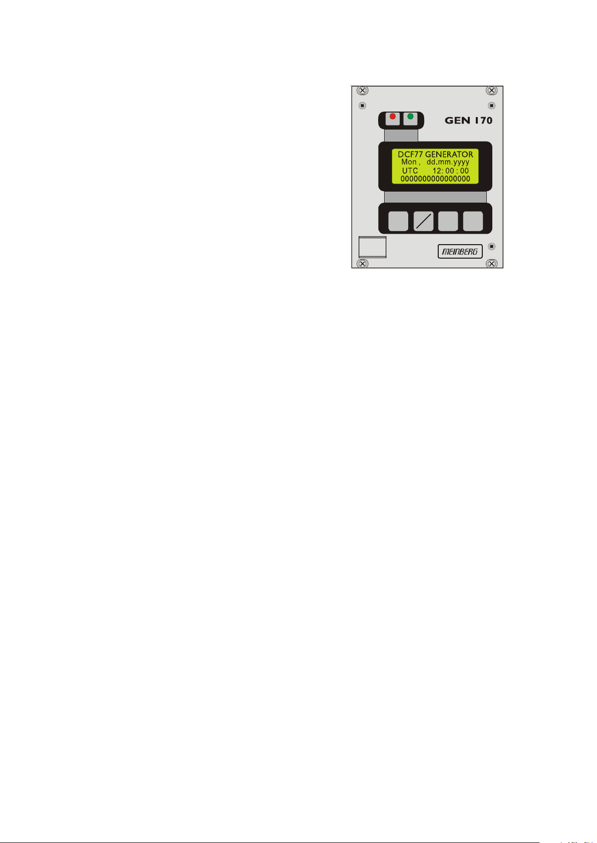
The GEN170 Front Panel Layout
FAIL LED and LOCK LED
The red LED labeled FAIL is turned on after power-up and stays on until the current
time has either been acknowledged via the ACK key in the front panel, or the time has
been set via the serial interface. The green LOCK LED reflects the generated DCF77
compatible AM time marks.
LC Display
The 4 x 16 character LC display is used to show the system's time and status and let the
user edit parameters. The keys described below let the user select the desired menu. The
next chapter lists all available menus in detail. A quick reference of the available menus
and submenus can be found at the end of this document.
MENU Key
This key lets the user step through several display menus showing specific data.
CLR/ACK Key
This key has to be used when parameters are to be modified. When this key is pressed
the parameters that have been edited are saved in the battery buffered memory. If the
menu is left without pressing CLR/ACK all changes are discarded.
NEXT Key
When editing parameters (LCD cursor is visible) this key moves the cursor to the next
digit rsp. to the next parameter to be edited. If the current menu just displays data (cursor
not visible) pressing this key switches to a submenu (if available).
INC Key
When editing parameters this key increments the digit or letter at the cursor position.
8
Page 9
The Menus in Detail
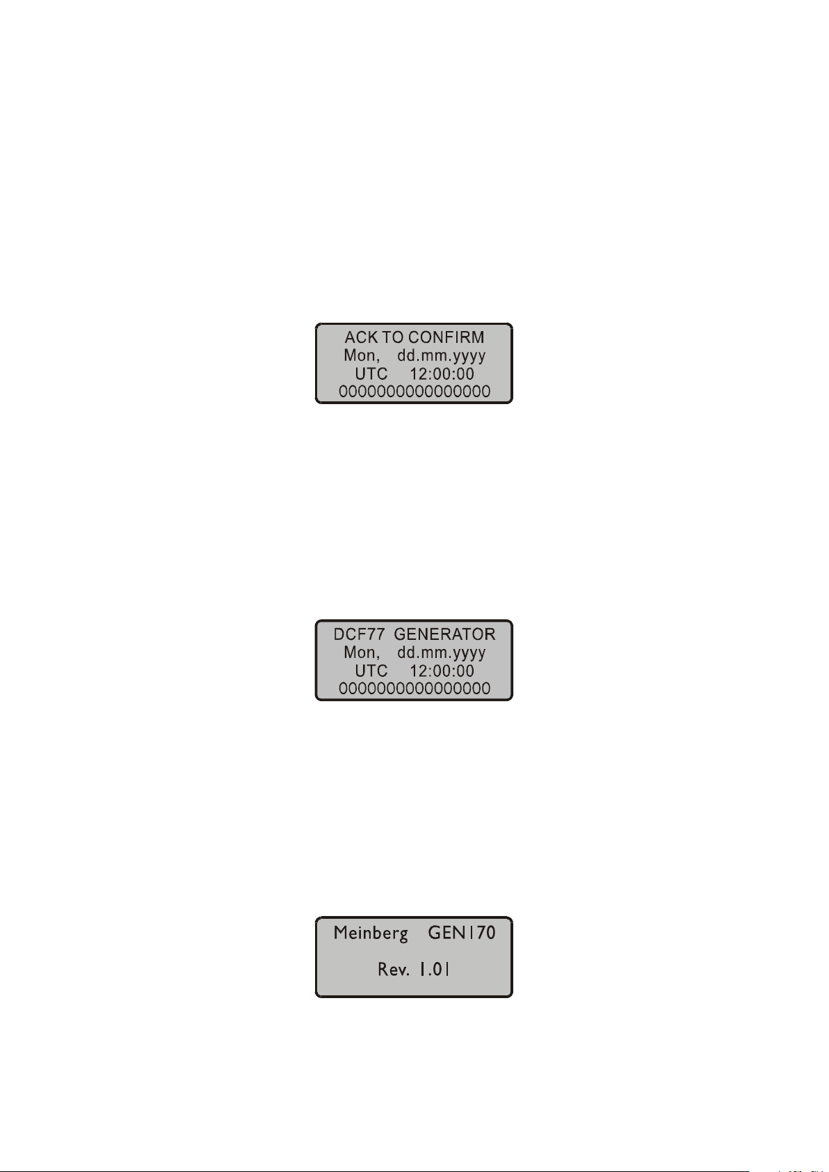
Root Menu
The root menu is shown when the receiver has completed initialization after powerup. During power-down the current date and time are kept in a battery buffered on-board
real time clock (RTC), so after power-up the initial calendar date and time should be
fairly correct. However, the red FAIL LED is on and a message is displayed asking to
acknowledge the initial time:
Unless the initial time is acknowledged by either pressing the CLR/ACK key in the
front panel or by setting the initial time via the RS-232 serial port the device stays in state
“unsynchronized“. This is to prevent the device from starting to distribute a wrong time
after power-up, which could otherwise happen due to interferences between an
incoming PPS pulse and the second changeover of the built-in RTC chip.
Once the initial time has been acknowledged the main menu is displayed. The first line
simply shows the module's function:
The next two lines display the current day of week, date, the name of the time zone
(just informational, as defined in the setup menu), and local time. The last line shows,
from left to right, the input levels of the control lines for the AM second marks 0 through
15. If a '1' is displayed a long time mark is generated at the corresponding second of a
minute, if a '0' is displayed, there will be a short mark at the corresponding second.
If the NEXT key is pressed in this menu, the display shows the module's firmware
version:
9
Page 10

Menu SETUP
From this menu, one of the configurable parameters can be selected using the NEXT
key. When the CLR/ACK key is pressed, a submenu is displayed which lets the user
view or modify the selected parameter. In each of these submenus the NEXT key lets the
cursor move to the next digit or letter to be edited whereas the INC key increments the
digit or letter under the cursor. If changes have been made, the CLR/ACK key must be
pressed in order to save those changes in the battery buffered memory, otherwise all
changes are discarded when the user presses the MENU key in order to return to the
SETUP display.
SETUP INITIAL TIME
Using this menu, GEN170's on-board real time clock can be set. When finally the
CLR/ACK button is pressed the system date and time is set to the values shown in the
display.
ADJUST SECONDS
If the system time differs by some seconds from an external reference time, this menu
can be used to adjust the internal clock to the reference time. The second and third lines
of the display show the system date and time, enabling the user to compare it to the
external time. The last line includes the two fields SEC+ and SEC-. The NEXT key can
be used to position the cursor on one of these fields. Each time the CLR/ACK key is
pressed, the system time is adjusted by one second: If the cursor is positioned on the
SEC+ field, the time is incremented by one second, otherwise it is decremented.
10
Page 11

SETUP TIME ZONE
This menu lets the user enter the names of the local time zone with daylight saving
disabled and enabled, together with the zones' time offsets from UTC. The left part of the
display shows the zone and offset if daylight saving is off whereas the right part shows
name and offset if daylight saving is on. These parameters are used to convert UTC to
local time, e.g. MEZ = UTC + 1h and MESZ = UTC + 2h for Central Europe. The zone
names are just informational and shown in the LC display. The range of date daylight
saving comes in effect can be entered using the next two topics of the setup menu.
SETUP DAYLIGHT SAV ON/OFF
The two topics let the user enter the range of date for daylight saving to be in effect.
Concerning parameter input both topics are handled identically, so they are described
together in this chapter. Beginning and end of daylight saving may either be defined by
exact dates for a single year or using an algorithm which allows the device to recompute
the effective dates year by year. The figures below show how to enter parameters in both
cases. If the number of the year is displayed as wildcards ('*'), a day-of-week must be
specified. Then, starting from the configured date, daylight saving changes the first day
which matches the configured day-of-week. In the figure below March 25, 1996 is a
Monday, so the next Sunday is March 31, 1996. If the number of the year is not
displayed as wildcards then the complete date exactly determines the day daylight saving
has to change (March 31, 1996 in the figures below), so the day-of-week doesn't need to
be specified and therefore is displayed as wildcards.
SETUP LEAP SECOND
11
Page 12

This menu can be used to enter the date of a leap second insertion. In order to adjust
the world wide time (UTC) to the earth rotation, the International Earth Rotation Service
(IERS) announces when a leap second must be inserted into the UTC time scale. The
IERS prefers to insert a leap second after 23:59:59 UTC on December, 31 or on June,
30, if necessary.
SETUP SERIAL PORT PARM
Using this topic the user can enter transmission speed and framing of the serial ports.
Default parameters are:
COM0: 19200 baud, 8N1
COM1: 9600 baud, 8N1
SETUP SER. STRING TYPE
This menu lets the user select the time string formats sent via the serial ports. As of this
writing the GEN170 supports sending the Meinberg standard string only on both ports.
12
Page 13

SETUP SERIAL OUTPUT
This menu lets the user select the serial ports' mode of operation. COM0 transmits the
current date and time using Meinberg's standard string. This string can be sent
automatically once per second, once per minute or on request by ASCII '?' only.
SETUP TIMECODE OUT
This menu lets the user configure the card's IRIG/AFNOR time code output. The
CODE: parameter selects the desired code frame format (IRIG or AFNOR), and the
TIME: parameter determines whether the transmitted code should carry UTC, or local
time.
Since most time code formats do neither include the UTC offset of the transmitted
time, nor a flag which reports the current DST status, the recommended setting is UTC in
order to avoid unexpected time steps of the connected time code receivers.
The IEEE1344 signal frame also contains a Time Figure Of Merit (TFOM) flag which
reflects whether the time code generator is synchronized, or not. If the IEEE1344 code is
selected then an additional parameter is displayed in the lower right corner which
determines whether the TFOM flag reports the real current synchronization status
(EN_T), or whether it always reports the generator was synchronized (DI_T). The latter
setting can be useful in testing scenarios.
13
Page 14

INIT USER PARMS
This menu lets the user reset all configurable parameters to default values. Before
initialization is done, the user must press CLR/ACK once more to acknowledge.
Resetting Factory Defaults
If both the NEXT key and the INC key on the front panel are pressed while the system
is powered up the battery buffered memory is cleared and user definable parameters are
reset to factory defaults. The key should be held until the root menu is displayed on LCD.
Attention: If the GEN170 module is assembled as one part of a larger equipment then
the default parameters may not be appropriate for the rest of the equipment. Please check
the new settings and make sure they match the settings required for the complete system.
Firmware Updates
Whenever the on-board software must be upgraded or modified, the new firmware
can be downloaded to the internal flash memory via the serial port COM0. There is no
need to open the metal case and insert a new EPROM.
If the MENU key on the front panel is pressed while the system is powered up, a
bootstrap-loader is activated and waits for instructions from the serial port COM0. The
new firmware can be uploaded from any standard PC with serial interface. A loader
program will be shipped together with the file containing the image of the new firmware.
The contents of the program memory will not be modified until the loader program has
sent the command to erase the flash memory. So if the MENU key is pressed
unintentionally while the system is powered up, the firmware will not be changed
accidentally. After the next power-up the system will be ready to operate again.
14
Page 15

Format of the Meinberg Standard Time String
The Meinberg Standard Time String is a sequence of 32 ASCII characters starting with
the STX (start-of-text) character and ending with the ETX (end-of-text) character. The
format is:
<STX>D:dd.mm.yy;T:w;U:hh.mm.ss;uvxy<ETX>
The letters printed in italics are replaced by ASCII numbers whereas the other characters
are part of the time string. The groups of characters as defined below:
<STX> Start-Of-Text (ASCII code 02h)
dd.mm.yy the current date:
dd day of month (01..31)
mm month (01..12)
yy year of the century (00..99)
w the day of the week (1..7, 1 = Monday)
hh.mm.ss the current time:
hh hours (00..23)
mm minutes (00..59)
ss seconds (00..59, or 60 while leap second)
uv clock status characters (depending on clock type):
u: ‘#’ GPS: clock is running free (without exact synchr.)
PZF: time frame not synchronized
DCF77: clock has not synchronized after reset
‘ ‘ (space, 20h)
GPS: clock is synchronous (base accuracy is reached)
PZF: time frame is synchronized
DCF77: clock has synchronized after reset
v: ‘*’ GPS: receiver has not checked its position
PZF/DCF77: clock currently runs on XTAL
‘ ‘ (space, 20h)
GPS: receiver has determined its position
PZF/DCF77: clock is syncronized with transmitter
x time zone indicator:
‘U’ UTC Universal Time Coordinated, formerly GMT
‘ ‘ MEZ European Standard Time, daylight saving disabled
‘S’ MESZ European Summertime, daylight saving enabled
y anouncement of discontinuity of time, enabled during last hour
before discontinuity comes in effect:
‘!’ announcement of start or end of daylight saving time
‘A’ announcement of leap second insertion
‘ ‘ (space, 20h) nothing announced
<ETX> End-Of-Text (ASCII code 03h)
15
Page 16

Time code
Principle of Operation
The Board GEN170 has been designed for the generation of IRIG, AFNOR and
IEEE1344 standard time codes. Apart from the digitally generated amplitude-modulated
code, it also provides the unmodulated DC-Level shift code. The modulated sine wave
carrier and the board´s internal time pattern are derived from the radio clock´s disciplined
oscillator.
Block Diagram Time code
modulated timecode
driver
50 unbalanced
D/A converter
modulator
high- and low-active
unmodulated timecodes
timecode
microcontroller
digital
sinewave
generator
EPLD
PPS
10 MHz
16
Page 17

IRIG Standard Format
x 3x
IRIB-B : 1000 Hz
binary 0 binary 1
TYPICAL MODULATED CARRIER IRIG-A : 10000 Hz
17
Page 18

AFNOR Standard Format
18
Page 19

Assignment of CF Segment in IEEE1344 mode
Bit No. Designation Description
49
Position Identifier P5
50 Year BCD encoded 1
51 Year BCD encoded 2
low nibble of BCD encoded year
52 Year BCD encoded 4
53 Year BCD encoded 8
54 empty, always zero
55 Year BCD encoded 10
56 Year BCD encoded 20
high nibble of BCD encoded year
57 Year BCD encoded 40
58 Year BCD encoded 80
59 Position Identifier P6
60 LSP - Leap Second Pending set up to 59s before LS insertion
61 LS - Leap Second 0 = add leap second, 1 = delete leap second
62 DS P - Da ylight Saving P e nding se t up t o 59s b efor e d a ylight s aving cha nge o ver
63 DS T - Da ylight Saving Time se t d ur ing d a ylight s a ving t ime
1.)
64 Timezone O ffset Sign sign of TZ offset 0 = '+', 1 = '-'
65 TZ Offset binary encoded 1
66 TZ Offset binary encoded 2
Offset from IRIG time to UTC time.
Encoded IRIG time plus TZ Offset equals UTC
67 TZ Offset binary encoded 4
a t a ll time s !
68 TZ Offset binary encoded 8
69 Position Identifier P7
70 TZ O ffs e t 0 . 5 hour se t if ad d it ion a l ha lf hour o ffs e t
71 TFOM Time figure of merit
72 TFOM Time figure of merit
time figure of merit represents approximated
clock error.
2.)
0x00 = clock locked
73 TFOM Time figure of merit
0x0F = clock failed
74 TFOM Time figure of merit
75 PARITY parity on all preceding bits incl. IRIG-B time
1.)
current firmware does not support deletion of leap seconds
2.)
TFOM is cleared, when clock is synchronized first after power up. see chapter Selection of generated timecode
19
Page 20

Generated Time codes
Besides the amplitude modulated sine wave signal, the board also provides unmodulated
DC-Level Shift TTL output in parallel. Thus six time codes are available.
a) B002: 100pps, PWM DC signal, no carrier
BCD time of year
b) B122: 100pps, AM sine wave signal, 1 kHz carrier frequency
BCD time of year
c) B003: 100pps, PWM DC signal, no carrier
BCD time of year, SBS time of day
d) B123: 100pps, AM sine wave signal, 1 kHz carrier frequency
BCD time of year, SBS time of day
e) B006: 100pps, PWM DC signal, no carrier
BCD time of year, year number ( 0...99 )
f) B126: 100pps, AM sine wave signal, 1 kHz carrier frequency
BCD time of year, year number ( 0...99 )
g) B007: 100pps, PWM DC signal, no carrier
BCD time of year, SBS time of day, year number ( 0...99 )
h) B127: 100pps, AM sine wave signal, 1 kHz carrier frequency
BCD time of year, SBS time of day, year number ( 0...99 )
i) AFNOR: Code according to NFS-87500, 100pps,
AM sine wave signal, 1kHz carrier frequency,
BCD time of year, complete date, SBS time-of-day,
Signal level according to NFS-87500
j) IEEE1344: Code according to IEEE1344-1995, 100pps,
AM sine wave signal, 1kHz carrier frequency,
BCD time-of-year, SBS time of day, IEEE1344
extensions for date, timezone, daylight-saving
and leap second in control functions (CF) segment.
see also table 'Assignment of CF segment in IEEE1344 mode'
20
Page 21

Selection of Generated Time Code
The time code to be generated can be selected by Menu Setup TIMECODE OUT.
DC-Level Shift Codes (PWM signal) B00x and modulated sine wave carrier B12x are
always generated simultaneously. Both signals are provided at the VG64-Connector,
i.e. if code B122 is selected also code B002 is available. This applies for the codes
AFNOR NFS 87-500 and IEEE1344 as well.
The TFOM field in IEEE1344 code is set dependent on the 'already sync'ed' character
('#') which is sent in the serial time telegram. This character is set, whenever the
preconnected clock was not able to synchronize after power up reset. The 'time figure of
merit' (TFOM) field is set as follows.
Clock synchronized once after power up : TFOM = 0000
Clock not synchronized after power up : TFOM = 1111
For testing purposes the output of TFOM in IEEE1344 mode can be disabled. The
segment is then set to all zeros.
Outputs
The module GEN170-TC provides modulated and unmodulated (DC-Level Shift)
outputs. The format of the time codes is illustrated "IRIG-" and "AFNOR standardformat".
AM Sine Wave Output
The amplitude-modulated carrier is available at the VG connector pin 6a. The carrier
frequency depends on the code and has a value of 1 kHz (IRIG-B). The signal amplitude
is 3Vpp (MARK) and 1Vpp (SPACE) into 50 Ω. The encoding is made by the number of
MARK amplitudes during ten carrier waves. The following agreements are valid:
a) binary "0" : 2 MARK amplitudes, 8 SPACE amplitudes
b) binary "1" : 5 MARK amplitudes, 5 SPACE amplitudes
c) position-identifier : 8 MARK amplitudes, 2 SPACE amplitudes
PWM DC Output
The pulse width modulated DC signals labeled "IRIG" and "AFNOR standard format"
are coexistent to the modulated output and is available at the VG connector pin 13a with
TTL level.
Technical Data
Outputs:
Unbalanced AM sine wave signal: 3VPP (MARK) / 1VPP (SPACE) into 50Ω
PWM signal: TTL (2,5V into 50Ω), active high
21
Page 22

Technical Specifications GEN170
LC DISPLAY : 4x16 character, menu selectable by push buttons
INPUT
SIGNALS : 1 pps in pulse per second (TTL level, leading edge)
10 MHz in reference frequency (Sine wave)
(only if configured for external reference)
amplitude V
input impedance: 50 Ohm
OUTPUT
SIGNALS : 10 MHz reference frequency (TTL level)
77.5 kHz carrier frequency (TTL-Pegel)
AM second mark (TTL level, active high)
PZF PRN sequence (TTL level)
PZF_CLK PRN clock (TTL level)
PZF_WIN PRN window (TTL level, active high)
IRIG_AC modulated IRIG sine wave output
IRIG_DC unmodulated IRIG output
P_SEC second pulse, duration 200ms (TTL level)
PPM minute pulse, duration 200ms (TTL level)
:1 V
eff
ACCURACY OF
PULSES : better than ±100 nsec
ACCURACY OF INTERNAL
XTAL : 1 day: ±1.10
1 year: ±5.10
drift with temparature: ±2.10
-7
-7
-7
SERIAL PORT : 2 asynchronous serial port (RS-232)
transmission speed: 300 through 19200
framing: 7N2, 7E1, 7E2, 8N1, 8N2, 8E1
default setting: 19200, 8N1
POWER
REQUIREMENTS : 5 V ± 5% @ 300 mA
PHYSICAL
DIMENSION : 19" module in a closed 112mm high x 102mm
wide closed aluminium case
FRONT
PANEL : 3U / 21HP (128mm high x 107mm wide), Aluminium
22
Page 23

REAR EDGE
CONNECTOR : according to DIN 41612, type C 64, rows a+c (male)
AMBIENT
TEMPERATURE : 0 ... 60° C
HUMIDITY : 85% max.
23
Page 24

Signal Description GEN170
Name Pin Function
GND 32a+c Ground
VCC in (+5V) 1a+c +5V supply
Vosc in (+5V) 2a+c +5V supply
10 MHz out 12a 10 MHz frequency output (TTL level)
2.25MHz out 27c 2,25MHz frequency output (TTL level)
77.5 kHz out 11a 77.5 kHz frequency output (TTL level)
DCF out 8c AM time marks (TTL level, active high)
PZF_CLK out 10a PRN clock (TTL level)
PZF_WIN out 7c PRN window (TTL level, active high)
PZF out 6c PRN sequence (TTL level)
P_SEC out 14c pulse once a second, duration 200ms (TTL level)
PPM out 8c pulse once a minute, duration 200ms (TTL level)
IRIG_AC out a6 Modulated IRIG sine wave output
IRIG_DC out a7 Unmodulated IRIG output
10MHz in 4c 10MHz reference input 1V
into 50 Ohm
eff
1 pps in 28c sync. second (TTL, rising edge)
TTL_INxx in control inputs for AM marks 0 through 15 (TTL)
long AM mark if input is high
COMx TxD out COMx RS-232 output
COMx RxD in COMx RS-232 input
/RESET in/out 9c RESET signal, Open Drain pulled up to +5V
(reserved) reserved, do not connect
24
Page 25

Rear Connector Pin Assignments GEN170
ac
10
11
12
13
14
15
16
17
1
2
3
4
5
6
7
8
9
VCC in (+5V) VCC in (+5V)
Vos c in ( +5V) Vosc in (+ 5V )
10 MHz in
IRIG_AC out PZF out
IRIG_DC out PZF_ WIN out
PPM DCF out
/RES ET in/out
PZF_CLK out
77.5 kHz out
10MHz out
TTL_I N 0 in
TTL_IN1 in P_SEC out
TTL_IN 2 in reserved 0
TTL_IN 3 in reserved 1
TTL_IN 4 in reserved 2
18
19
20
21
22
23
24
25
26
27
28
29
30
31
32
TTL_I N 5 in
TTL_IN 6 in reserved 3
TTL_I N 7 in
TTL_I N 8 in
TTL_I N 9 in
TTL_I N 1 0 in
TTL_I N 11 in CO M1 TxD o ut
TTL_I N 1 2 in
TTL_I N 1 3 in CO M 0 TxD o ut
TTL_I N 1 4 in 2, 2 5M Hz o ut
TTL_I N 1 5 in 1 p p s in
COM1 RxD in
COM0 RxD in
GND GND
25
Page 26

DCF77-Simulator
Function
Together with a DCF generator GEN170 the module generates an amplitude
modulated time signal which is compatible with the signal spread by the german long
wave transmitter DCF77.
The GEN170 generates TTL time marks which are 100msec in lenght if a binary "0"
is to be transmitted resp. 200msec if a binary "1" is transmitted. These time marks are
used by the SIM77PV4 to modulate the on board generated 77.5kHz sine wave carrier
according to the DCF77 transmitter.
This DCF77 compatible signal is accessible via four DC insulated outputs which can
be connected to all Meinberg AM radio clocks directly. The signal can be distributed by
additional antenna amplifiers/distributors.
10MHz
1MHz
PZF_IN
MOD_IN
power
Internal
Oscillator
Power
select
Modulator
Programmable
Logic Devive
clock
77,5kHz
DCF_OUT
DCF_OUT
DCF_OUT
DCF_OUT
26
Page 27

Technical Specifications SIM77PV4
Power Req.: +5V / @70mA
Input: MOD in (DCF77 time marks) and 1MHz in, TTL level
optional: 10MHz in (solder bridges on the board have to be set
correspondingly)
Outputs: 4x amplitude modulated, DC insulated carrier (77.5 kHz)
Output level: approx. -60 dBm
Output level: approx. -50 dBm (requires modifications)
Connector: 64 pin rear VG edge connector DIN41612
Dimension: Eurocard, 100mm x 160mm, 1.5mm Epoxy
Front Panel: 4HP/3U (20mm wide x 128.4mm high)
Amb. Temperature: 0° ... 50°C
Humidity: 85% max.
27
Page 28

Rear Connector Pin Assignments SIM77PV4
ac
1 VCC in (+5V) VCC in (+5V)
2
3
4 MOD in
5
6PZF in
7
8
9
10 +SIM_OUT1
11 1MHz in
12 10MHz in -SIM_OUT1
13
14
15
16 +SIM_OUT2
17
18 -SIM_OUT2
19
20
21
22 +SIM_OUT3
23
24 -SIM_OUT3
25
26
27 7.75MHz in
28 +SIM_OUT4
29
30 -SIM_OUT4
31
32 GND GND
male connector according to DIN 41612, type C 64, rows a + c
28
Page 29

GEN170TGP Rear view
y
1
13
Assignments of the 25 pin Connector
14
25
Made in German
29
Page 30

30
 Loading...