

Page 1

Technical Information
Operating Instructions
FDM509
Page 2

Impressum
Meinberg Funkuhren GmbH & Co. KG
Auf der Landwehr 22
D-31812 Bad Pyrmont
Phone: +49 (0) 52 81 / 9309-0
Fax: +49 (0) 52 81 / 9309-30
Internet: http://www.meinberg.de
Email: info@meinberg.de
March 8, 2006
Page 3

Table of Contents
Impressum ............................................................................................ 2
Generally .............................................................................................. 5
Functional Principle ............................................................................. 5
The Front Panel Layout ....................................................................... 6
LED PL Time ............................................................................. 6
LED REF Time........................................................................... 6
LED Overflow ............................................................................ 6
LED Fail ..................................................................................... 6
Push Button Reset ....................................................................... 6
Mains Socket Power Line (optional) .......................................... 7
Installation FDM509 ............................................................................ 7
Power Supply .............................................................................. 7
Input Signals ............................................................................... 7
Powering Up the System ............................................................ 7
Configuration ....................................................................................... 8
Power Line Frequency ................................................................ 8
Average and Serial Output String .............................................. 8
Initialize Power Line Time ......................................................... 8
Output String .............................................................................. 9
The serial RS232 ports ............................................................. 10
Analog Output .......................................................................... 10
Serial Reset Command ....................................................................... 10
Error Bits ............................................................................................ 11
Analog Values .................................................................................... 11
Page 4

Firmware Updates .............................................................................. 12
Inquiring Serial Number and Software Revision ............................... 12
CE Label ............................................................................................ 12
Technical Specifications FDM509..................................................... 14
Format of the Meinberg Standard Time String ........................ 15
Rear Connector Pin Descriptions ............................................. 16
Rear Connector Pin Descriptions ............................................. 17
Component Layout ................................................................... 19
Page 5

Generally
The module FDM509 was designed to calculate and monitor the frequency in 50/60Hz
power line networks. A preconnected reference is necessary that provides a high
accuracy 10MHz frequency, a serial time string and a PPS (pulse per second).
Additional to the frequency the "PLT" (Power Line Time) is calculated that would be
displayed by a clock using the mains frequency as its timekeeping reference. The
accumulated differece between the drifting power line time and the high accuracy
reference time (REF) is called "time deviation". Because the time deviation has the
long-term accuracy of the reference it is suitable to supervise the frequency stability.
The time deviation can be read out either via the serial interface or via one of the two
integrated analog outputs for further evaluation or regulation.
Functional Principle
The power line frequency to be monitored is applied via the rear VG edge connector
(optional: via a mains socket in the frontpanel) of the FDM509, then filtered and
transformed. After that the sine-wave signal is converted into a TTL signal using a
schmitt trigger. The rising edge of the TTL signal is used to start/stop a counter that is
clocked by the high accuracy 10MHz pulse of the reference. Because of that the period
length of the mains frequency is measured with a resolution of 100ns and read out by
the micro controller of the FDM509. The values are averaged over a period of one
second or one minute (selectable) and then the frequency is calculated with a resolution of 1mHz.
Calculation of the PL time occurs by counting the periods of the power line
frequency. Depending on the nominal frequency the PL time seconds are incremented
after counting 50 or 60 periods. To initialize the PL time it is necessary to get the exact
time via the serial interface. The time deviation is calculated once per second or once
per minute and is limited to ±100 seconds.
5
Page 6
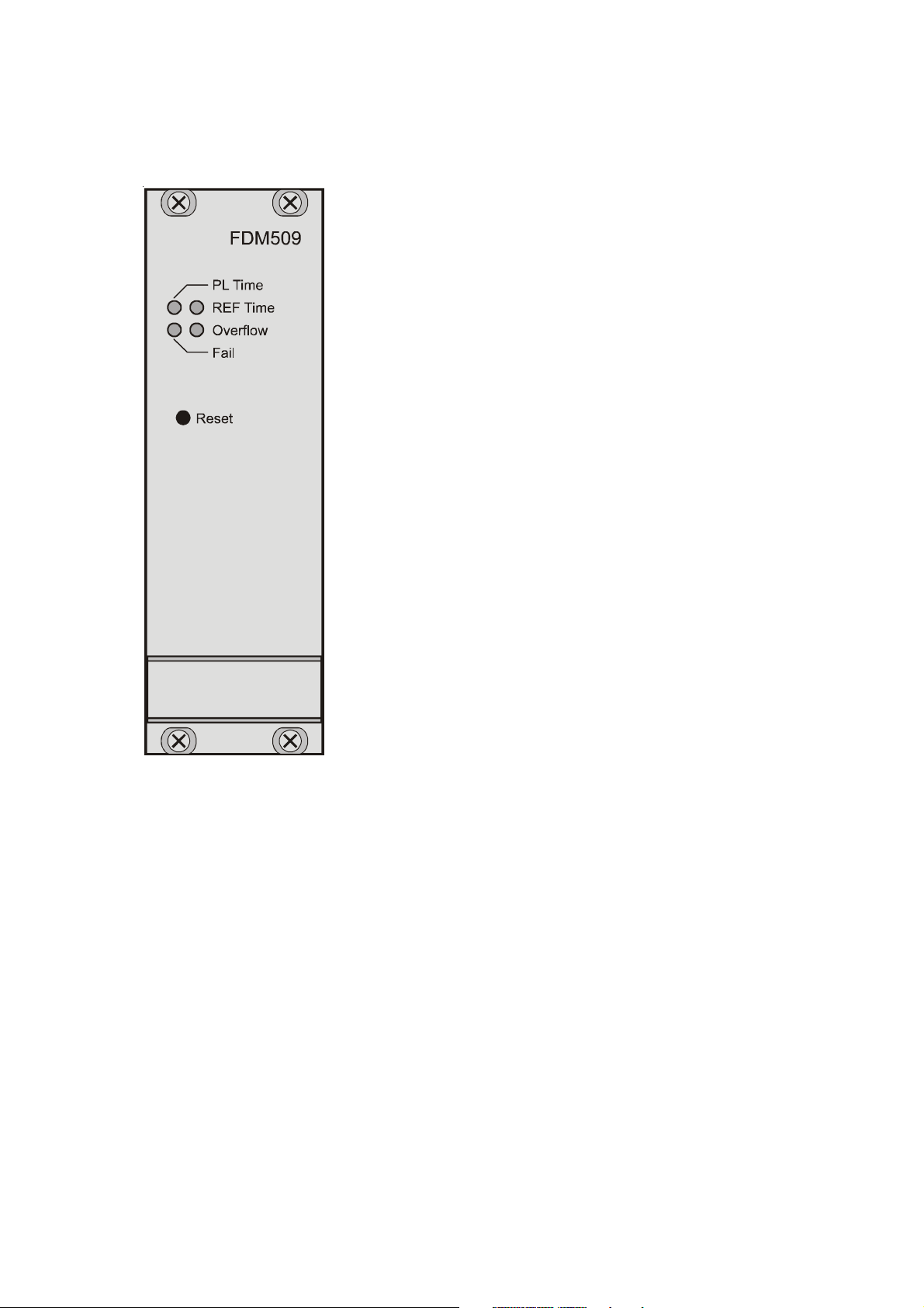
The Front Panel Layout
The 40.6mm wide front panel integrates four LED
indicators and a covered push button.
LED PL Time
This LED toggles once per second corresponding to
the power line time seconds when the mains frequency is detected correctly. It stops toggling if either the
mains frequency or the 10MHz reference is not applied or the REF time could not be read out after reset.
LED REF Time
This LED toggles once per second corresponding to
the pulse per second of the reference. It stops toggling if either the PPS or the 10MHz reference is not
applied or the REF time could not be read out after
reset.
LED Overflow
This LED is switched on when the time deviation
(the difference between REF time and PL time) exceeds the limit of ±100 seconds. It is switched off
again when either the time deviation is dropped below ±100 seconds or a reset sets the time deviation
back to zero.
LED Fail
This LED is switched on if correct operation of the module is not ensured and the
results are unusable. Loosing the PPS or the 10MHz from the referenc could be a
reason for this as well as an error in reading in the REF time. The serial output of the
measure string is stopped when this LED is switched on.
Push Button Reset
The time deviation is set to zero if this covered key is pressed for one second at least.
Furthermore the PL time is initialized with the REF time, provided that a time string is
applied to the serial port COM1 and the corresponding DIP switch is set. If not, both
the PL time and the REF time are set to 00:00:00. Also all error bits are cleared and the
analog outputs are set to their initial state (0V). Pressing the reset key has the same
effect than causing a hardware power-up reset or sending a serial reset command.
6
Page 7

Mains Socket Power Line (optional)
The power line frequency to be monitored may be connected to the module via this
optional power socket in the front panel instead of the rear VG edge connector. The
power supply for the FDM509 occurs not via this applied mains voltage but via the
rear edge connector (+5V). To detect the mains frequency of 45 ... 65 Hz correctly the
voltage of the connected mains must be in the range of 70V ... 270V AC. This input is
protected by a 200mA slow blowing fuse.
Installation FDM509
Power Supply
FDM509 requests only one single supply voltage of +5V, connected via the rear edge
connector of the module. The current consumption is about 180mA.
Input Signals
For operation of the frequency deviation monitor FDM509 the following input signals, provided by a preconnected reference, are necessary:
a) 10MHz oscillator clock, TTL level, rear edge connector pin Z12
b) pulse per second PPS, TTL level, rear edge connector pin D6
c) time string (RS232), rear edge connector pin B10
A GPS receiver GPS167 or a DCF77 radio clock PZF509 can be used as a reference,
for example.
Powering Up the System
If all the input signals, the power supply and the power line to be monitored have been
connected, the system is ready to operate. The Fail LED as well as the REF Time LED
and the PL Time LED are switched on after power up reset. FDM509 waits for the
incoming serial time string via COM1 to initialize the internal system time (REF
time). After this is done the PL time is also initialized with the REF time. From now
on the REF time is incremented with the PPS applied while the PL time is incremented
by a certain number of recorded mains frequency periods (50 or 60). The REF Time
LED and the PL Time LED start toggling once per second corresponding to their time
base. The Fail LED is switched off.
7
Page 8

Configuration
Configuration occurs via the on board DIL switch. To synchronize the FDM509 it is
necessary to set baudrate and framing of the connected reference time string to 19200
baud, 8N1. The module starts sending the measure string as soon as all necessary
signals are applied and the Fail LED is switched off.
Power Line Frequency
FDM509 is designed to monitor the frequency in 50Hz mains as well as in 60Hz
mains. The corresponding configuration is set via DIL-SW1:
DIL-SW1 (nominal mains frequency) OFF: 50Hz ON: 60Hz
Average and Serial Output String
The period length of the mains frequency is measured and then read out by the micro
controller of the FDM509. The values are averaged over a period of one second or one
minute and then the frequency is calculated with this average value. The serial string is
sent once per second or once per minute, too, corresponding to the period of average.
Configuration occurs via DIL-SW2:
DIL-SW2 (Average) OFF: once per second ON: once per minute
Initialize Power Line Time
The PL time must be initialized at the beginning of the measurement, so it either can
be set with the REF time or it starts with 00:00:00. In the first case the REF time is
read in via COM1 (19200 baud, 8N1) of the FDM509, PL time and REF time are
synchrounous at the beginning of the measurement. Because only the difference
between the REF time and the drifting PL time is actually relevant, reading in the REF
time string and connecting the serial ports may be omited. In this case both times start
with 00:00:00 after reset.
DIL-SW3 (initialialize PL time) OFF: time string ON: 00:00:00
8
Page 9

Output String
One of two different output strings containing the results of the measurement can be
selected to be sent via the serial port COM0. The first string is a sequence of 62 ASCII
characters containing the frequency F, the frequency deviation FD, the REF time, the
power line time PL and the time deviation TD, seperated by a space character each.
The string ends with the characters Carriage-Return (ASCII code 0Dh) and Line-Feed
(ASCII code 0Ah). The letters displayed in italics are replaced by the calculated
values whereas the other characters are part of the string:
F:49.984_FD:-00.016_REF:15:03:30_PLT:15:03:30.378_TD:+00.378<CR><LF>
The second string is a sequence of 23 ASCII characters containing only information
about frequency deviation FD and time deviation TD, seperated by a space character:
FD:-00.016_TD:+00.378<CR><LF>
Selection of the string type occurs via DIL-SW4:
DIL-SW4 (string type) OFF: long ON: short
The meaning of the several values are described below:
F:49.984 The measured power line frequency with a resolution of 1mHz.
The accuracy of the displayed value is ±1mHz.
FD:-00.016 The frequency deviation is the difference between the measured
frequency and the nominal mains frequency (50Hz or 60Hz).
This value is signed, it has the same accuracy and resolution as
the frequency.
REF:15:03:30 The time from the preconnected reference. This time is read in
via COM1 RxD once after reset (if connected, otherwise set to
00:00:00) and then incremented by the PPS of the referenc.
Time jumps, like changeover in daylight saving or leap seconds,
will not be executed.
PLT:15:03:30.378 The power line time is synchronized with the REF time once
after reset and then incremented by a certain number of recorded mains frequency periods (50 or 60). In addition the PL time
milliseconds are shown, too.
TD:+00.378 The time deviation is the difference between the drifting PL
time and the exact REF time. This value is signed, with a resolution of 1ms. The time deviation is set to 00.000 after reset. It has
the long-term accuracy of the PPS from the reference.
9
Page 10

The serial RS232 ports
Baudrate and framing of the serial port COM0 can be configured using the DILswitches SW5 and SW6:
DIL-SW5 (Baudrate) OFF: 19200 baud ON: 9600 baud
DIL-SW6 (Framing) OFF: 8N1 ON: 7E2
COM1 RxD is used to read in the time string of the reference. This serial port is fixed
configured to 19200 baud, 8N1. The connected reference must be configured appropriate and send the time string once per second. The TxD line of COM1 is sending the
long output string once per second. It can be used to connect a display, for example.
Analog Output
FDM509 provides two analog outputs for longtime-recording. These outputs have a
range of -2.5V ... +2.5V, divided in 65536 steps. Either the frequency deviation or the
time deviation can be selected for monitoring via one of these analog outputs. The full
scale range of the analog outputs can be set either to 500mHz or to 5Hz (i.e. 0,2mHz/
mV or 2mHz/mV) when the frequency deviation is selected, or, if the time deviation is
selected, to 10s or to 100s (i.e. 4ms/mV or 40ms/mV). Configuration regarding the
analog outputs occurs via the DIL-switches SW7 to SW10:
DIL-SW7 (source for A1) OFF: frequency deviation ON: time deviation
DIL-SW8 (full scale range A1) OFF: 5Hz/ 100s ON: 500mHz/10s
DIL-SW9 (source for A2) OFF: frequency deviation ON: time deviation
DIL-SW10 (full scale range A2) OFF: 5Hz/100s ON: 500mHz/10s
Serial Reset Command
The FDM509 can be reseted to its start values by a serial command. Sending the
character 'R' (ASCII code 52h) via the serial port COM0 causes a reset that has the
same effect than powering up the system or pressing the Reset button (refer to chapter
"Push Button Reset").
10
Page 11

Error Bits
FDM509 provides eight error bits that can be read out via the serial port COM0 by
sending the character 'E' (ASCII code 45h). Any error bit reports a corresponding
error event that occurs during operation. The format is:
ERROR:X
X
X
X
X
X
X
8
7
6
5
4
X1<CR><LF>
3
2
The meaning of the error bits is:
X1: Fail (equal to LED Fail), an error occured and the serial output is stopped,
can be cleared only by a reset
X2: No Time String, FDM509 waits for the serial time string
X3: No 10MHz, missing reference clock, can be cleared only by a reset
X4: No PPS, no pulse per second, can be cleared only by a reset
X5: No Power Line, a mains frequency can not be detected,
can be cleared only by a reset
X6: Time Deviation Overflow (equal to LED Overflow), time deviation > ±100s
X7: A1 Overflow, analog output 1 has reached its full scale range
X8: A2 Overflow, analog output 2 has reached its full scale range
The error bits can be red out during normal operation as well as after an error occurs
and the serial output is stopped. In the second case the last measure string before the
output was stopped will be sent out once more, additional to the error bits.
Analog Values
The values of the two analog outputs provided by FDM509 can also be red out via the
serial port COM0 by sending the character 'A' (ASCII code 41h). FDM509 sends a
string with the following format:
A1:XXXX_A2:XXXX<CR><LF>
The values are given in hex code (0000h ... FFFFh). The initial state is 8000h.
11
Page 12

Firmware Updates
Whenever the on-board software must be upgraded or modified, the new firmware can
be downloaded to the internal flash memory via the serial port COM0.
If the key "Reset" in the front panel is pushed down while the system is powered up,
a bootstrap-loader will be activated that waits for instructions from the serial port
COM0. The new firmware can be sent to the FDM509 from any standard PC with
serial interface. A loader program will be shipped together with the file containing the
image of the new firmware.
The contents of the program memory will not be modified until the loader program
has sent the command to erase the flash memory. So if the "Reset" key is pushed down
unintentionally while the system is powered up, the firmware will not be changed
accidentially. After the next power-up, the system will be ready to operate again.
Inquiring Serial Number and Software Revision
The serial number and the revision of the loaded software can be read out by sending
the three characters "SN!" via COM0 to the clock that starts sending the following
string:
SN:FDM509 9041260 REV:01.10/01
The software revision is updated automatically with every update of the firmware. The
serial number is fixed in an I2C bus EEPROM and can not be changed.
CE Label
This device conforms to the directive 89/336/EWG on the
approximation of the laws of the Member States of the European
Community relating to electromagnetc compatibility.
12
Page 13

13
Page 14

Technical Specifications FDM509
INPUT SIGNALS: 10MHz oscillator clock (TTL level)
pulse per second, activ high (TTL level)
serial time string (RS232), 19200 baud, 8N1 (see "Format
of the Meinberg Standard Time String")
mains voltage, 70V... 270V, 45Hz ... 65Hz (protected with
200mA fuse, slow blowing)
OUTPUTS: 2 analog outputs: -2,5V ... 2,5V, resolution: 16 bit
fail output (TTL level)
overflow output (TTL level)
SERIAL
RS232 PORTS: 2 serial RS232 ports, COM1: 19200 baud, 8N1
COM0 configurable via DIL-switch:
Baudrate: 9600 or 19200 baud
Framing: 7E2 or 8N1
output and average once per second or once per minute
output string: one of two different formats selectable, see chap-
ter "Output String"
ACCURACY OF
MEASUREMENT: frequency: accuracy of reference (10MHz) ±1mHz
time deviation: accuracy of reference (PPS) ±1ms
CONNECTORS: rear VG edge connector, mixed F/H, DIN 41612
Type F: 24 poles, type H: 7 poles
optional: mains socket in the front panel
POWER
REQUIREMENTS: +5V, @180mA
PHYSICAL
DIMENSIONS: Eurocard, 100mm x 160mm, 1.5mm Epoxy
FRONT PANEL: 3U / 8HP (128mm high x 40.6mm wide), Aluminium
AMBIENT
TEMPERATURE: 0 ... 50°C
HUMIDITY: max. 85 %
OPTIONS: power line input via mains socket in the front panel
Hardware and software modifications accordding to customer
specification
14
Page 15

Format of the Meinberg Standard Time String
The Meinberg Standard Time String is a sequence of 32 ASCII characters starting
with the STX (start-of-text) character and ending with the ETX (end-of-text) character. The format is:
<STX>D:dd.mm.yy;T:w;U:hh.mm.ss;uvxy<ETX>
The letters printed in italics are replaced by ASCII numbers whereas the other
characters are part of the time string. The groups of characters as defined below:
<STX> Start-Of-Text (ASCII code 02h)
dd.mm.yy the current date:
dd day of month (01..31)
mm month (01..12)
yy year of the century (00..99)
w the day of the week (1..7, 1 = Monday)
hh.mm.ss the current time:
hh hours (00..23)
mm minutes (00..59)
ss seconds (00..59, or 60 while leap second)
uv clock status characters (depending on clock type):
u: ‘#’ GPS: clock is running free (without exact synchr.)
PZF: time frame not synchronized
DCF77: clock has not synchronized after reset
‘ ‘ (space, 20h)
GPS: clock is synchronous (base accuracy is reached)
PZF: time frame is synchronized
DCF77: clock has synchronized after reset
v: ‘*’ GPS: receiver has not checked its position
PZF/DCF77: clock currently runs on XTAL
‘ ‘ (space, 20h)
GPS: receiver has determined its position
PZF/DCF77: clock is syncronized with transmitter
x time zone indicator:
‘U’ UTC Universal Time Coordinated, formerly GMT
‘ ‘ MEZ European Standard Time, daylight saving disabled
‘S’ MESZ European Summertime, daylight saving enabled
y anouncement of discontinuity of time, enabled during last hour
before discontinuity comes in effect:
‘!’ announcement of start or end of daylight saving time
‘A’ announcement of leap second insertion
‘ ‘ (space, 20h) nothing announced
<ETX> End-Of-Text (ASCII code 03h)
15
Page 16

Rear Connector Pin Descriptions
Signal Name Pin Description
VCC in (+5V) B, D+Z2 +5V supply voltage
GND B, D+Z16 power supply ground
/Reset Z4 Reset and Boot signal for starting bootstrap loader
(pull down while powering-up)
signal is parallel wired to push button "Reset"
P_SEC in D6 pulse per second input, TTL level, active high
10 MHz in Z12 10 MHz oscillator clock input, TTL-Pegel
COM0 TxD out D8 COM0 RS232 transmit data output
COM0 RxD in B8 COM0 RS232 receive data input
COM0 GND Z6 COM0 ground (=power supply ground)
COM1 TxD out D10 COM1 RS232 transmit data output
COM1 RxD in B10 COM1 RS232 receive data input
COM1 GND B12 COM1 ground (=power supply ground)
A1 out B4 analog output no. 1
A2 out B6 analog output no. 2
A_out GND D4 analog output ground (=power supply ground)
SDA D14 reserved for extensions
SCL Z14 reserved for extensions
SCL_EN B14 reserved for extensions
Fail out Z8 fail output (Fail LED), TTL level
Overflow out D12 overflow output (Overflow LED), TTL level
Reserve in Z10 input, reserved for extensions
L1 Z28 L, mains voltage
N D30 N, mains voltage
PE Z32 PE, protective earth conductor
16
Page 17

Rear Connector Pin Descriptions
ZBD
2 VCC in (+5V) VCC in (+5V) VCC in (+5V)
4 /Reset A1 out GND
6 GND A2 out P_SEC in
8 Fail out RxD0 TxD0
10 Reserve in RxD1 TxD1
12 10MHz in GND Overflow out
14 SCL SCL_EN SDA
16 GND GND GND
20
22
24
26
28 L1
30 N
32 PE
17
Page 18

18
Page 19

Component Layout
19
Page 20

 Loading...