

Page 1
Page 2

PCI-DAS1200/JR
Multifunction Analog Input and Digital I/O
User's Guide
Document Revision 6, March, 2009
© Copyright 2009, Measurement Computing Corp.
Page 3

HM PCI-DAS1200_JR.doc
Trademark and Copyright Information
Measurement Computing Corporation, InstaCal, Universal Library, and the Measurement Computing logo are
either trademarks or registered trademarks of Measurement Computing Corporation. Refer to the Copyrights &
Trademarks section on mccdaq.com/legal for more information about Measurement Computing trademarks.
Other product and company names mentioned herein are trademarks or trade names of their respective
companies.
© 2009 Measurement Computing Corporation. All rights reserved. No part of this publication may be
reproduced, stored in a retrieval system, or transmitted, in any form by any means, electronic, mechanical, by
photocopying, recording, or otherwise without the prior written permission of Measur
Corporation.
Notice
Measurement Computing Corporation does not authorize any Measurement Computing Corporation product for
use in life support systems and/or devices without prior written consent from Measurement Computing
Corporation. Life support devices/systems are devices or systems that, a) are intended for surgical implantation
into the body, or b) support or sustain life and whose failure to perform can be reasonably expected to result in
injury. Measurement Computing Corporation products are not designed with the components required, and are
not subject to the testing required to ensure a level of reliability suitable for the treatment and diagnosis of
people.
ement Computing
2
Page 4

3 4
Page 5

Table of Contents
Preface
About this User's Guide ....................................................................................................................... 5
What you will learn from this user's guide ......................................................................................................... 5
Conventions in this user's guide ......................................................................................................................... 5
Where to find more information ......................................................................................................................... 5
Register-level programming ............................................................................................................................... 6
Chapter 1
Introducing the PCI-DAS1200/JR ........................................................................................................ 7
Overview: PCI-DAS1200/JR features ................................................................................................................ 7
Software features ................................................................................................................................................ 7
PCI-DAS1200/JR block diagram ....................................................................................................................... 8
Chapter 2
Installing the PCI-DAS1200/JR ............................................................................................................ 9
What is included with your PCI-DAS1200/JR ................................................................................................... 9
Hardware .......................................................................................................................................................................... 9
Additional documentation ................................................................................................................................................. 9
Optional components ........................................................................................................................................................ 9
Unpacking the PCI-DAS1200/JR ..................................................................................................................... 10
Installing the software ...................................................................................................................................... 10
Installing the hardware ..................................................................................................................................... 10
Configuring the hardware ................................................................................................................................. 11
Differential input mode ....................................................................................................................................................11
Single-ended input mode .................................................................................................................................................11
Connecting the board for I/O operations .......................................................................................................... 11
Connectors, cables – main I/O connector ......................................................................................................... 12
Pin out – main I/O connector ...........................................................................................................................................13
Field wiring and signal termination accessories ...............................................................................................................15
Chapter 3
Calibrating the board .......................................................................................................................... 16
Introduction ...................................................................................................................................................... 16
Calibration theory ............................................................................................................................................. 16
Chapter 4
Specifications ...................................................................................................................................... 17
Analog input ..................................................................................................................................................... 17
Digital input/output........................................................................................................................................... 18
Counter section ................................................................................................................................................. 18
Power consumption .......................................................................................................................................... 19
Environmental .................................................................................................................................................. 19
Main connector and pin out .............................................................................................................................. 19
8-channel differential mode pin out .................................................................................................................................20
16-channel single-ended mode pin out.............................................................................................................................21
Declaration of Conformity .................................................................................................................. 22
Page 6
About this User's Guide
What you will learn from this user's guide
This user's guide explains how to install, configure, and use the PCI-DAS1200/JR board so that you get the
most out of the analog input and digital I/O features.
This user’s guide also refers you to related documents available on our web site, and to technical support
resources.
Conventions in this user's guide
For more information on …
Text presented in a box signifies additional information and helpful hints related to the subject matter you are
reading.
Caution! Shaded caution statements present information to help you avoid injuring yourself and others,
damaging your hardware, or losing your data.
Preface
< : > Angle brackets that enclose numbers separated by a colon signify a range of numbers, such as those assigned
to registers, bit settings, etc.
bold text Bold text is used for the names of objects on the screen, such as buttons, text boxes, and check boxes. For
example:
1. Insert the disk or CD and click the OK button.
italic text Italic text is used for the names of manuals and help topic titles, and to emphasize a word or phrase. For
example:
The InstaCal® installation procedure is explained in the Quick Start Guide.
Never touch the exposed pins or circuit connections on the board.
Where to find more information
The following electronic documents provide helpful information relevant to the operation of the PCIDAS1200/JR board.
MCC's Specifications: PCI-DAS1200/JR (the PDF version of the Specifications chapter in this guide) is
available on our web site at www.mccdaq.com/pdfs/Specs/PCI-DAS1200-JR-spec.pdf.
MCC's Quick Start Guide is available on our web site at
MCC's Guide to Signal Connections is available on our web site at
www.mccdaq.com/signals/signals.pdf.
MCC's Universal Library User's Guide is available on our web site at
MCC's Universal Library Function Reference is available on our web site at
MCC's Universal Library for LabVIEW™ User’s Guide is available on our web site at
PCI-DAS1200/JR User's Guide (this document) is also available on our web site at
5
Page 7

PCI-DAS1200/JR User's Guide About this User's Guide
Register-level programming
You should use the Universal Library to control your board. Only experienced programmers should try register-
level programming. If you need to program at the register level in your application, refer to the Register Map
for the PCI-DAS1200 Series. This document is available at www.mccdaq.com/registermaps/RegMapPCI-
DAS1200-JR.pdf.
6
Page 8

Chapter 1
Introducing the PCI-DAS1200/JR
Overview: PCI-DAS1200/JR features
This manual explains how to install and use the PCI-DAS1200/JR board. The PCI-DAS1200/JR board is a
multifunction measurement and control board designed for the PCI bus.
The PCI-DAS1200/JR provides eight differential or 16 single-ended 12-bit analog inputs, with sample rates of
up to 330 kHz. Input ranges are either bipolar or unipolar. Bipolar input ranges are ±10V, ±5V, ±2.5V, and
±1.25V. Unipolar input ranges are 0 to 10V, 0 to 5V, 0 to 2.5V, and 0 to 1.25V. All input ranges are softwareselectable.
The PCI-DAS1200/JR has 24-bits of parallel, digital I/O as two 8-bit ports and two 4-bit ports. Each port can be
configured independently as input or output.
The PCI-DAS1200/JR board contains an 82C54 counter chip, which consists of three 16-bit counters. Clock,
gate, and output signals from two of the three counters are available on a 100-pin I/O connector. The third
counter is used internally.
Software features
For information on the features of InstaCal and the other software included with your PCI-DAS1200/JR, refer
to the Quick Start Guide that shipped with your device. The Quick Start Guide is also available in PDF at
Check www.mccdaq.com/download.htm for the latest software version or versions of the software supported
under less commonly used operating systems.
7
Page 9

PCI-DAS1200/JR User's Guide Introducing the PCI-DAS1200/JR
Digital I/O
8
PCI
CONTROLLER
BADR1
BADR2
BADR3
BADR4
Interrupt
Boot
EEPROM
ADC
Pacer
Control
Scan
&
Burst
Logic
DAC
Control
Trigger
Control
Decode/Status
Int
Ctl
Bus
Timing
INT
Gains = 1, 2, 4, 8
XTRIG
CONTROLLER
FPGA
ADC
Pacer
CTR 2
CTR 1
Sample
Counter
CTR0
Control
Gain and Offset Autocal
INT
12-Bit, 330KHz
Mux
&
Gain
Analog In
16 CH S.E.
8 CH DIFF.
1024 x 12
FIFO
CTR1
ADC
Index
Counter
User
CTR 0
Control
Time Base
GATE
CLK
OUT
INT
XTRIG
Start EOC
INT
10 MHz
PCI Bus(5V, 32-bit, 33 MHZ)
Burst/Scan
Burst/Scan
EXT PCR
10 MHz
CTR2
CLK2
GATE2
OUT2
CLK1
GATE1
OUT1
FIRSTPORTA
FIRSTPORTB
Control
FIRSTPORTCH
FIRSTPORTA(7:0)
FIRSTPORTB(7:0)
FIRSTPORTCH(3:0)
FIRSTPORTCL(3:0)
FIRSTPORTCL
Local Bus
PCI-DAS1200 and PCI-DAS1200/JR
block diagram
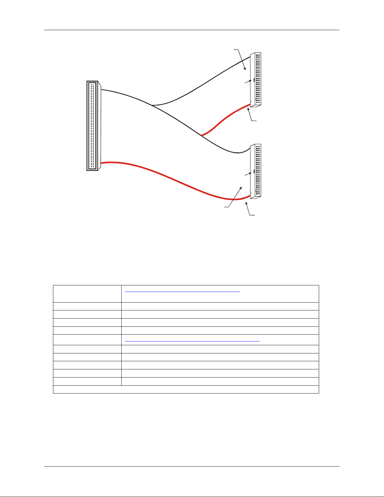
PCI-DAS1200/JR block diagram
PCI-DAS1200/JR functions are illustrated in the block diagram shown here.
Figure 1. PCI-DAS1200/JR functional block diagram
8
Page 10

Installing the PCI-DAS1200/JR
What is included with your PCI-DAS1200/JR
As you unpack your board, make sure each of the items shown below is included:
Hardware
PCI-DAS1200/JR board
Chapter 2
Additional documentation
In addition to this hardware user's guide, you should also receive the Quick Start Guide (available in PDF at
the software you received with your PCI-DAS1200/JR and information regarding installation of that software.
Please read this booklet completely before installing any software or hardware.
Optional components
If you ordered any of the following products with your board, they should be included with your shipment.
C100FF-x cable
9
Page 11

PCI-DAS1200/JR User's Guide Installing the PCI-DAS1200/JR
Signal termination and conditioning accessories
MCC provides signal termination products for use with the PCI-DAS1200/JR. Refer to Field wiring and
signal termination accessories on page 15 for a complete list of compatible accessory products.
Unpacking the PCI-DAS1200/JR
As with any electronic device, you should take care while handling to avoid damage from static
electricity. Before removing the PCI-DAS1200/JR from its packaging, ground yourself using a wrist strap or by
simply touching the computer chassis or other grounded object to eliminate any stored static charge.
If any components are missing or damaged, notify Measurement Computing Corporation immediately by
phone, fax, or e-mail:
Phone: 508-946-5100 and follow the instructions for reaching Tech Support.
Fax: 508-946-9500 to the attention of Tech Support
Email: techsupport@mccdaq.com
Installing the software
Quick-Start.pdf.
Installing the hardware
PCI-DAS1200/JR board is completely plug-and-play. There are no switches or jumpers to set. Configuration is
controlled by your system's BIOS. To install your board, follow the steps below:
Install the MCC DAQ software before you install your board
The driver needed to run your board is installed with the MCC DAQ software. Therefore, you need to install the
MCC DAQ software before you install your board. Refer to the Quick Start Guide for instructions on installing
the software.
1. Turn your computer off, open it up, and insert your board into an available PCI slot.
2. Close your computer and turn it on.
If you are using an operating system with support for plug-and-play (such as Windows 2000 or Windows
XP), a dialog box pops up as the system loads indicating that new hardware has been detected. If the
information file for this board is not already loaded onto your PC, you will be prompted for the disk
containing this file. The MCC DAQ software contains this file. If required, insert the Measurement
Computing Data Acquisition Software CD and click OK.
3. To test your installation and configure your board, run the InstaCal utility you installed in the previous
Software-Quick-Start.pdf for information on how to initially set up and load InstaCal.
Allow your computer to warm up for at least 15 minutes before acquiring data with this board. The high speed
components used on the board generates heat, and it takes this amount of time for a board to reach steady state
if it has been powered off for a significant amount of time.
10
Page 12

PCI-DAS1200/JR User's Guide Installing the PCI-DAS1200/JR
Configuring the hardware
All hardware configuration options on the PCI-DAS1200/JR are software controlled. You can select some of
the configuration options using InstaCal, such as the analog input configuration (16 single-ended or eight
differential channels) and the source for the two independent counters. Once selected, any program that uses the
Universal Library will initialize the hardware according to these selections.
Differential input mode
When all channels are configured for differential input mode, eight analog input channels are available. In this
mode, the input signal is measured with respect to the low input. The input signal is delivered through three
wires:
The wire carrying the signal to be measured connects to CH# IN HI.
The wire carrying the reference signal connects to CH# IN LO.
The third wire is connected to LLGND.
Differential input mode is the preferred configuration for applications in noisy environments, or when the signal
source is referenced to a potential other than PC ground.
Single-ended input mode
When all channels are configured for single-ended input mode, 16 analog input channels are available. In this
mode, the input signal is referenced to the board’s signal ground (LLGND). The input signal is delivered
through two wires:
The wire carrying the signal to be measured connects to CH# IN HI.
The second wire is connected to LLGND.
Connecting the board for I/O operations
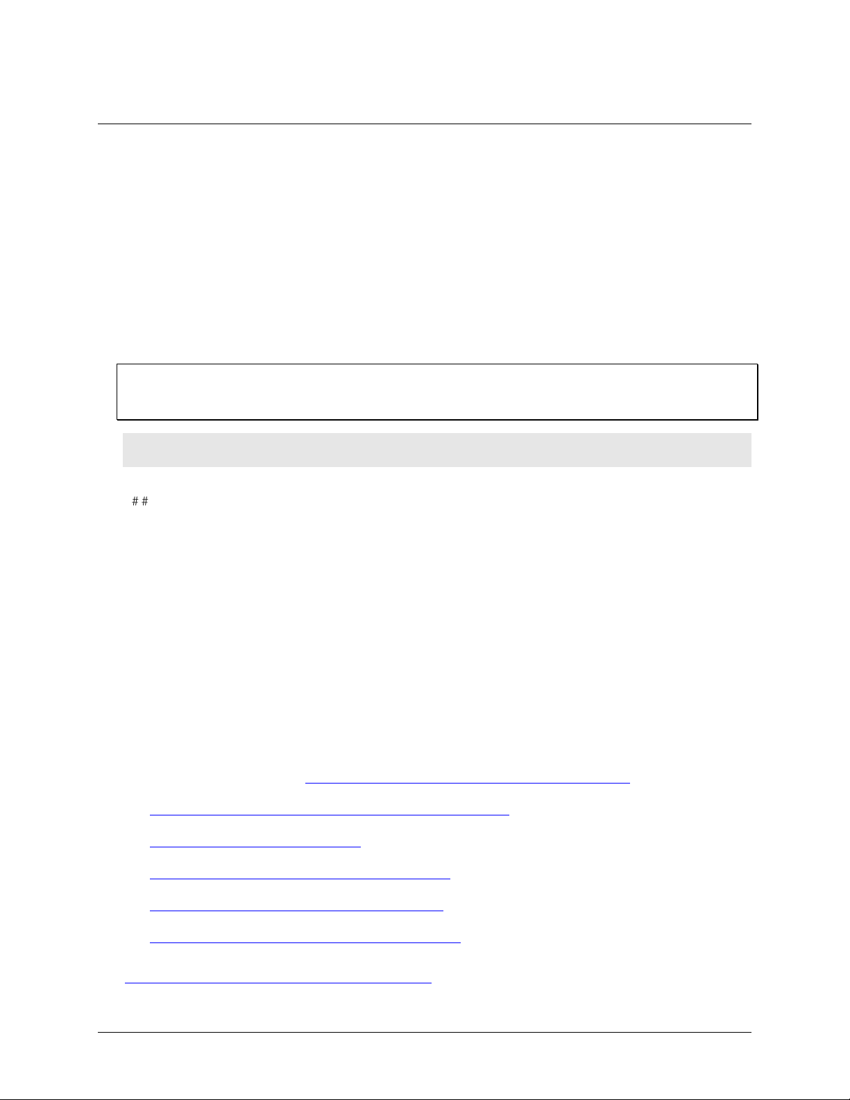
All I/O signals are brought through a 100-pin high-density connector. The C100FF-x cable is used to connect
field signals to the board. This cable has a pair of 50-pin ribbon cables that are joined at one end to a 100-pin
connector. The first 50-pin cable (pins 1-50) carries the analog signals. The second 50-pin cable (pins 51-100)
carries the digital signals. The 100-pin connector mates with the PCI-DAS1200/JR connector. The two 50-pin
ribbon cables are terminated with standard 50-pin header connectors.
11
Page 13

PCI-DAS1200/JR User's Guide Installing the PCI-DAS1200/JR
Connector type
100-pin high density
Compatible cable
C100FF-x, unshielded ribbon cable. x = length in feet (Figure 2)
Compatible accessory products
(with C100FF-x cable)
ISO-RACK16/P
CIO-ERB08*
CIO-ERB24*
CIO-SERB24*
SSR-RACK08*
SSR-RACK24*
BNC-16SE
BNC-16DI
CIO-MINI50 (2 required)
CIO-TERM100 (1 required)
SCB-50 (1 required)
* These devices require the DADP-5037 PCI-DAS to 37-pin SSR and ERB adapter board.
The CIO-ERB08 device also requires the TN-MC78M05CT voltage regulator.
Connectors, cables – main I/O connector
The table below lists the board connectors, applicable cables and compatible accessory boards.
Board connectors, cables, accessory equipment
12
Page 14

PCI-DAS1200/JR User's Guide Installing the PCI-DAS1200/JR
Signal Name
Pin Pin
Signal Name
GND
100
50
GND
N/C
99
49
N/C
N/C
98
48
PC +5V
N/C
97
47
N/C
N/C
96
46
N/C
A/D Internal Pacer
95
45
A/D External Trigger IN
N/C
94
44
N/C
N/C
93
43
N/C
-12V
92
42
A/D External Pacer
GND
91
41
CTR4 OUT
+12V
90
40
CTR4 GATE
GND
89
39
CTR4 CLK
N/C
88
38
N/C
CTR5 OUT
87
37
N/C
CTR5 GATE
86
36
N/C
CTR5 CLK
85
35
N/C
N/C
84
34
N/C
N/C
83
33
N/C
CTR6 OUT
82
32
N/C
CTR6 GATE
81
31
N/C
CTR6 CLK
80
30
N/C
N/C
79
29
N/C
N/C
78
28
N/C
N/C
77
27
N/C
N/C
76
26
N/C
N/C
75
25
N/C
FIRSTPORTC Bit 7
74
24
N/C
FIRSTPORTC Bit 6
73
23
N/C
FIRSTPORTC Bit 5
72
22
N/C
FIRSTPORTC Bit 4
71
21
N/C
FIRSTPORTC Bit 3
70
20
N/C
FIRSTPORTC Bit 2
69
19
N/C
FIRSTPORTC Bit 1
68
18
LLGND
FIRSTPORTC Bit 0
67
17
CH7 IN LO
FIRSTPORTB Bit 7
66
16
CH7 IN HI
FIRSTPORTB Bit 6
65
15
CH6 IN LO
FIRSTPORTB Bit 5
64
14
CH6 IN HI
FIRSTPORTB Bit 4
63
13
CH5 IN LO
FIRSTPORTB Bit 3
62
12
CH5 IN HI
FIRSTPORTB Bit 2
61
11
CH4 IN LO
FIRSTPORTB Bit 1
60
10
CH4 IN HI
FIRSTPORTB Bit 0
59
9
CH3 IN LO
FIRSTPORTA Bit 7
58
8
CH3 IN HI
FIRSTPORTA Bit 6
57
7
CH2 IN LO
FIRSTPORTA Bit 5
56
6
CH2 IN HI
FIRSTPORTA Bit 4
55
5
CH1 IN LO
FIRSTPORTA Bit 3
54
4
CH1 IN HI
FIRSTPORTA Bit 2
53
3
CH0 IN LO
FIRSTPORTA Bit 1
52
2
CH0 IN HI
FIRSTPORTA Bit 0
51
1
LLGND
PCI slot ↓
Pin out – main I/O connector
8-channel differential mode pin out
13
Page 15

PCI-DAS1200/JR User's Guide Installing the PCI-DAS1200/JR
Signal Name
Pin Pin
Signal Name
GND
100
50
PC GND
N/C
99
49
N/C
N/C
98
48
PC +5V
N/C
97
47
N/C
N/C
96
46
N/C
A/D Internal Pacer Output
95
45
A/D External Trigger
N/C
94
44
N/C
N/C
93
43
N/C
-12V
92
42
A/D External Pacer
GND
91
41
OUT 4
+12V
90
40
GATE 4
GND
89
39
CLK 4
N/C
88
38
N/C
CTR5 OUT
87
37
N/C
CTR5 GATE
86
36
N/C
CTR5 CLK
85
35
N/C
N/C
84
34
N/C
N/C
83
33
N/C
CTR6 OUT
82
32
N/C
CTR6 GATE
81
31
N/C
CTR6 CLK
80
30
N/C
N/C
79
29
N/C
N/C
78
28
N/C
N/C
77
27
N/C
N/C
76
26
N/C
N/C
75
25
N/C
FIRSTPORTC Bit 7
74
24
N/C
FIRSTPORTC Bit 6
73
23
N/C
FIRSTPORTC Bit 5
72
22
N/C
FIRSTPORTC Bit 4
71
21
N/C
FIRSTPORTC Bit 3
70
20
N/C
FIRSTPORTC Bit 2
69
19
N/C
FIRSTPORTC Bit 1
68
18
LLGND
FIRSTPORTC Bit 0
67
17
CH15 IN
FIRSTPORTB Bit 7
66
16
CH7 IN
FIRSTPORTB Bit 6
65
15
CH14 IN
FIRSTPORTB Bit 5
64
14
CH6 IN
FIRSTPORTB Bit 4
63
13
CH13 IN
FIRSTPORTB Bit 3
62
12
CH5 IN
FIRSTPORTB Bit 2
61
11
CH12 IN
FIRSTPORTB Bit 1
60
10
CH4 IN
FIRSTPORTB Bit 0
59
9
CH11 IN
FIRSTPORTA Bit 7
58
8
CH3 IN
FIRSTPORTA Bit 6
57
7
CH10 IN
FIRSTPORTA Bit 5
56
6
CH2 IN
FIRSTPORTA Bit 4
55
5
CH9 IN
FIRSTPORTA Bit 3
54
4
CH1 IN
FIRSTPORTA Bit 2
53
3
CH8 IN
FIRSTPORTA Bit 1
52
2
CH0 IN
FIRSTPORTA Bit 0
51
1
LLGND
PCI slot ↓
16-channel single-ended mode pin out
All I/O signals are brought through a 100-pin high-density connector. You can use a C100FF-x to connect field
signals to the board (Figure 2). This cable has a pair of 50-pin ribbon cables joined at one end to a 100-pin
connector. The first 50-pin cable (pins 1-50) carries the analog signals. The second 50-pin cable (pins 51-100)
carries the digital signals. The 100-pin connector mates with the PCI-DAS1200/JR connector. The two 50-pin
ribbon cables are terminated with standard 50-pin header connectors.
Information on signal connections
General information regarding signal connection and configuration is available in the Guide to Signal
Connections. This document is available on our web site at www.mccdaq.com/signals/signals.pdf).
14
Page 16
PCI-DAS1200/JR User's Guide Installing the PCI-DAS1200/JR
1
50
2
49
51
100
52
99
10050
511
Key
Key
The red stripe
identifies pin # 1
The red stripe
identifies pin # 51
Cable is labeled
“Pins 51-100”.
Cable is labeled
“Pins 1-50”.
Screw terminal and
BNC adapters
http://www.mccdaq.com/products/accessories.aspx
SCB-50
50-conductor, shielded signal connection box.
CIO-MINI50
50-pin universal screw terminal accessory.
BNC-16SE
16-channel single-ended BNC connector box.
BNC-16DI
Eight-channel differential BNC connector box.
Signal conditioning
http://www.mccdaq.com/products/signal_conditioning.aspx
ISO-RACK16/P
16-channel isolation module mounting rack.
SSR-RACK24*
24-position solid state relay rack.
SSR-RACK08*
Eight-channel solid state relay rack.
CIO-ERB24*
24-channel electromechanical relay accessory for digital I/O boards.
CIO-ERB08*
Eight-channel electromechanical relay accessory for digital I/O boards.
* These devices require the DADP-5037 PCI-DAS to 37-pin SSR and ERB adapter board.
Figure 2. C100FF-x cable
Field wiring and signal termination accessories
The table below lists the MCC screw terminal and signal conditioning boards that are compatible with the PCIDAS1200/JR.
15
Page 17
PGIA
Analog In
A/D
Trim DAC
Coarse
Trim DAC
Fine
Pre-Gain
Offset
Variable
Gain
Chapter 3
Calibrating the board
Introduction
Calibrate the board using InstaCal after the board has fully warmed up. The recommended warm-up time is
15 minutes. For best results, calibrate the board immediately before making critical measurements. The high
resolution analog components on the board are sensitive to temperature. Pre-measurement calibration ensures
that your board is operating at optimum calibration values.
Calibration theory
The PCI-DAS1200/JR is shipped fully calibrated from the factory. Calibration coefficients are stored in
nvRAM. When using the Universal Library at run time, these calibration factors are loaded into system memory
and automatically retrieved each time you specify a different DAC/ADC range.
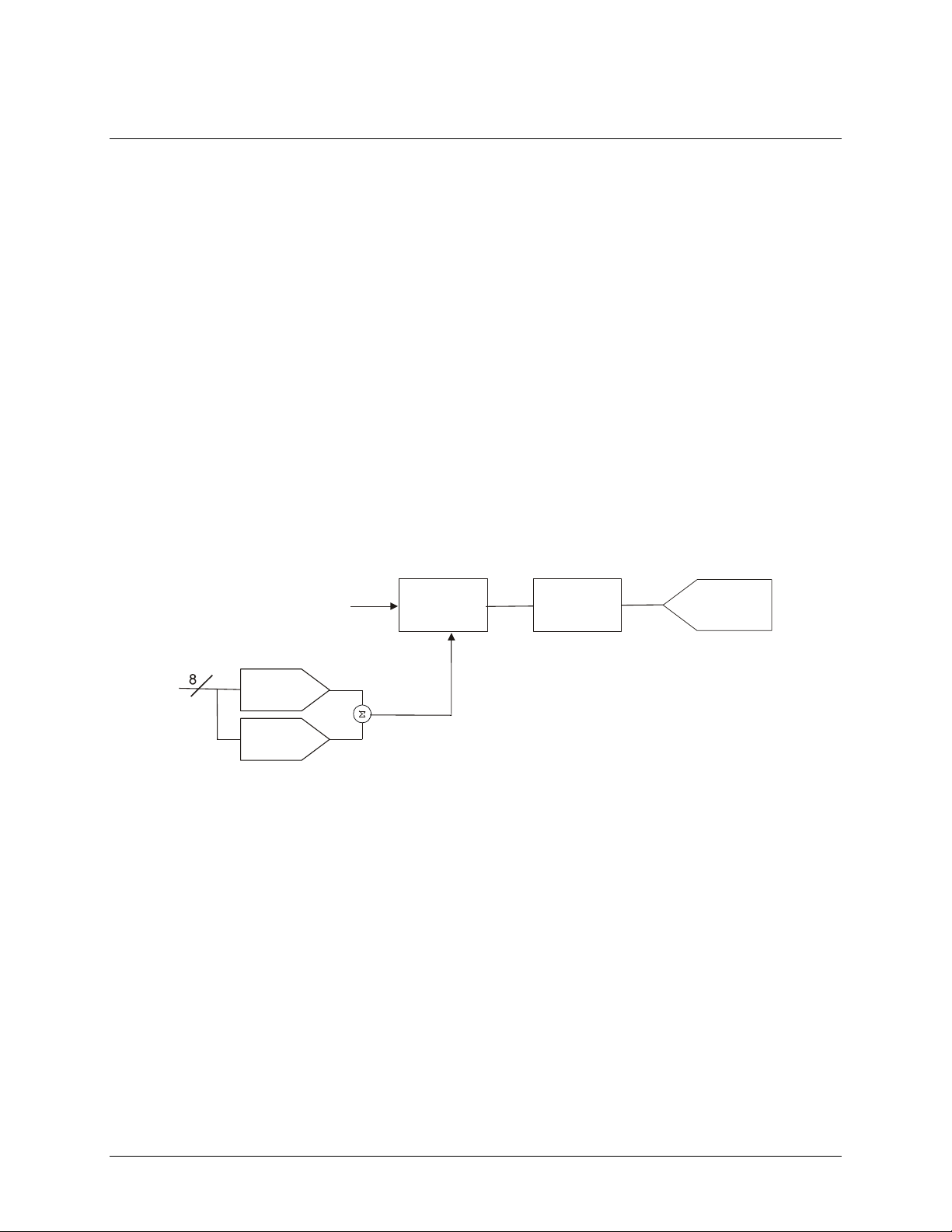
The analog input circuits are calibrated for offset and gain (Figure 3).
Offset calibration for the analog input is performed directly on the input amplifier (PGIA) with coarse and
fine trim DACs acting on the amplifier.
For input gain calibration, a precision calibration reference is used with coarse and fine trim DACs acting
on the ADC.
Figure 3. Analog input circuit calibration diagram
16
Page 18

Parameter
Specification
A/D converter type
7800
Resolution
12 bits
Number of channels
8 differential or 16 single-ended, software selectable
Input ranges
Bipolar: ±10 V, ±5 V, ±2.5 V, ±1.25 V
Unipolar: 0 to 10 V, 0 to 5 V, 0 to 2.5 V, 0 to 1.25 V
Software selectable
A/D pacing
Programmable: internal counter or external source (A/D External Pacer) or
software polled
Burst mode
Software selectable option, burst rate = 3 µs
A/D trigger sources
External digital: A/D External Trigger
A/D triggering modes
External digital: Software enabled, rising edge, hardware trigger
Pre-trigger: Unlimited pre- and post-trigger samples. Total # of
samples must be > 512.
Data transfer
From 1024 sample FIFO via REPINSW, interrupt or software polled
A/D conversion time
3 µs
Throughput
330 kHz min
Relative accuracy
±1.5 LSB
Differential linearity error
±0.75 LSB
Integral linearity error
±0.5 LSB typ, ±1.5 LSB max
Gain error (relative to calibration reference)
± 0.02% of reading max
No missing codes guaranteed
12 bits
Gain drift (A/D specs)
±6 ppm/°C
Zero drift (A/D specs)
±1 ppm/°C
Common mode range
±10 V
CMRR @ 60 Hz
70 dB
Input leakage current
200 nA
Input impedance
10 MOhm, min
Absolute maximum input voltage
±35 V
Noise distribution:
Rate = 1-330 KHz, average % ± 2 bins, average % ±1 bin, average # bins
All ranges: 100% / 100% / 3 bins
Specifications
Typical for 25 °C unless otherwise specified.
Specifications in italic text are guaranteed by design.
Analog input
Table 1. Analog input specifications
Chapter 4
17
Page 19

PCI-DAS1200/JR User's Guide Specifications
Parameter
Specification
Digital type
82C55A
Configuration
2 banks of 8, 2 banks of 4, programmable by bank as input or output
Number of I/O
24 (FIRSTPORTA 0 through FIRSTPORTC 7)
Output high
3.0 volts @ -2.5 mA min
Output low
0.4 volts @ 2.5 mA max
Input high
2.0 volts min, Vcc+0.5 volts absolute max
Input low
0.8 volts max, GND-0.5 volts absolute min
Power-up / reset state
Input mode (high impedance)
Interrupts
INTA# - mapped to IRQn via PCI BIOS at boot-time
Interrupt enable
Programmable
Interrupt sources
Residual counter, End-of-channel-scan, AD-FIFO-not-empty, AD-FIFO-half-full
Parameter
Specification
Counter type
82C54
Configuration
Two 82C54 devices. 3 down counters per 82C54, 16 bits each
82C54A:
Counter 0 - ADC residual
sample counter.
Source: ADC Clock.
Gate: Internal programmable source.
Output: End-of-Acquisition interrupt.
Counter 1 - ADC pacer lower
divider
Source: 10 MHz oscillator
Gate: tied to counter 2 gate, programmable source.
Output: chained to counter 2 clock.
Counter 2 - ADC pacer upper
divider
Source: counter 1 output.
Gate: Tied to counter 1 gate, programmable source.
Output: ADC pacer clock (if software selected), available at user connector.
82C54B:
Counter 0 - pretrigger mode
Source: ADC clock
Gate: external trigger
Output: End-of-Acquisition interrupt
Counter 0 - user counter 4
(when in non-pretrigger mode)
Source: User input at 100-pin connector (CLK4) or internal 10 MHz (software
selectable)
Gate: user input at 100-pin connector (GATE4)
Output: available at 100-pin connector (OUT4)
Counter 1 - user counter 5
Source: user input at 100-pin connector (CLK5)
Gate: user input at 100-pin connector (GATE5)
Output: available at 100-pin connector (OUT5)
Counter 2 - user counter 6
Source: user input at 100-pin connector (CLK6)
Gate: user input at 100-pin connector (GATE6)
Output: available at 100-pin connector (OUT6)
Clock input frequency
10 MHz max
High pulse width (clock input)
30 ns min
Low pulse width (clock input)
50 ns min
Gate width high
50 ns min
Gate width low
50 ns min
Input low voltage
0.8 V max
Digital input/output
Table 2. DIO specifications
Counter section
Table 3. Counter specifications
18
Page 20

PCI-DAS1200/JR User's Guide Specifications
Parameter
Specification
Input high voltage
2.0 V min
Output low voltage
0.4 V max
Output high voltage
3.0 V min
Parameter
Specification
+5 V operating
(A/D converting to FIFO)
0.8 A typical, 1.0 A max
Parameter
Specification
Operating temperature range
0 to 70 °C
Storage temperature range
-40 to 100 °C
Humidity
0 to 90% non-condensing
Connector type
100-pin high density
Compatible cable
C100FF-x, unshielded ribbon cable. x = length in feet
Compatible accessory products
(with C100FF-x cable)
ISO-RACK16/P
CIO-ERB08 (DADP-5037 adaptor and TN-MC78M05CT voltage regulator required *)
CIO-ERB24 (DADP-5037 adaptor required *)
CIO-SERB24 (DADP-5037 adaptor required)
SSR-RACK08 (DADP-5037 adaptor required *)
SSR-RACK24 (DADP-5037 adaptor required *)
BNC-16SE
BNC-16DI
CIO-MINI50 (2 required)
CIO-TERM100 (1 required)
SCB-50 (1 required)
Power consumption
Table 4. Power consumption specifications
Environmental
Table 5. Environmental specifications
Main connector and pin out
Table 6. I/O connector specifications
* Details on the DADP-5037 adaptor board are available on our web site at
www.mccdaq.com/products/cables-adapters.aspx.
19
Page 21

PCI-DAS1200/JR User's Guide Specifications
Pin
Signal Name
Pin
Signal Name
1
LLGND
51
FIRSTPORTA Bit 0
2
CH0 IN HI
52
FIRSTPORTA Bit 1
3
CH0 IN LO
53
FIRSTPORTA Bit 2
4
CH1 IN HI
54
FIRSTPORTA Bit 3
5
CH1 IN LO
55
FIRSTPORTA Bit 4
6
CH2 IN HI
56
FIRSTPORTA Bit 5
7
CH2 IN LO
57
FIRSTPORTA Bit 6
8
CH3 IN HI
58
FIRSTPORTA Bit 7
9
CH3 IN LO
59
FIRSTPORTB Bit 0
10
CH4 IN HI
60
FIRSTPORTB Bit 1
11
CH4 IN LO
61
FIRSTPORTB Bit 2
12
CH5 IN HI
62
FIRSTPORTB Bit 3
13
CH5 IN LO
63
FIRSTPORTB Bit 4
14
CH6 IN HI
64
FIRSTPORTB Bit 5
15
CH6 IN LO
65
FIRSTPORTB Bit 6
16
CH7 IN HI
66
FIRSTPORTB Bit 7
17
CH7 IN LO
67
FIRSTPORTC Bit 0
18
LLGND
68
FIRSTPORTC Bit 1
19
N/C
69
FIRSTPORTC Bit 2
20
N/C
70
FIRSTPORTC Bit 3
21
N/C
71
FIRSTPORTC Bit 4
22
N/C
72
FIRSTPORTC Bit 5
23
N/C
73
FIRSTPORTC Bit 6
24
N/C
74
FIRSTPORTC Bit 7
25
N/C
75
N/C
26
N/C
76
N/C
27
N/C
77
N/C
28
N/C
78
N/C
29
N/C
79
N/C
30
N/C
80
CTR6 CLK
31
N/C
81
CTR6 GATE
32
N/C
82
CTR6 OUT
33
N/C
83
N/C
34
N/C
84
N/C
35
N/C
85
CTR5 CLK
36
N/C
86
CTR5 GATE
37
N/C
87
CTR5 OUT
38
N/C
88
N/C
39
CTR4 CLK
89
GND
40
CTR4 GATE
90
+12V
41
CTR4 OUT
91
GND
42
A/D EXTERNAL PACER
92
-12V
43
N/C
93
N/C
44
N/C
94
N/C
45
A/D EXTERNAL TRIGGER IN
95
A/D INTERNAL PACER OUTPUT
46
N/C
96
N/C
47
N/C
97
N/C
48
PC +5V
98
N/C
49
N/C
99
N/C
50
GND
100
GND
8-channel differential mode pin out
20
Page 22

PCI-DAS1200/JR User's Guide Specifications
Pin
Signal Name
Pin
Signal Name
1
LLGND
51
FIRSTPORTA Bit 0
2
CH0 IN
52
FIRSTPORTA Bit 1
3
CH8 IN
53
FIRSTPORTA Bit 2
4
CH1 IN
54
FIRSTPORTA Bit 3
5
CH9 IN
55
FIRSTPORTA Bit 4
6
CH2 IN
56
FIRSTPORTA Bit 5
7
CH10 IN
57
FIRSTPORTA Bit 6
8
CH3 IN
58
FIRSTPORTA Bit 7
9
CH11 IN
59
FIRSTPORTB Bit 0
10
CH4 IN
60
FIRSTPORTB Bit 1
11
CH12 IN
61
FIRSTPORTB Bit 2
12
CH5 IN
62
FIRSTPORTB Bit 3
13
CH13 IN
63
FIRSTPORTB Bit 4
14
CH6 IN
64
FIRSTPORTB Bit 5
15
CH14 IN
65
FIRSTPORTB Bit 6
16
CH7 IN
66
FIRSTPORTB Bit 7
17
CH15 IN
67
FIRSTPORTC Bit 0
18
LLGND
68
FIRSTPORTC Bit 1
19
N/C
69
FIRSTPORTC Bit 2
20
N/C
70
FIRSTPORTC Bit 3
21
N/C
71
FIRSTPORTC Bit 4
22
N/C
72
FIRSTPORTC Bit 5
23
N/C
73
FIRSTPORTC Bit 6
24
N/C
74
FIRSTPORTC Bit 7
25
N/C
75
N/C
26
N/C
76
N/C
27
N/C
77
N/C
28
N/C
78
N/C
29
N/C
79
N/C
30
N/C
80
CTR6 CLK
31
N/C
81
CTR6 GATE
32
N/C
82
CTR6 OUT
33
N/C
83
N/C
34
N/C
84
N/C
35
N/C
85
CTR5 CLK
36
N/C
86
CTR5 GATE
37
N/C
87
CTR5 OUT
38
N/C
88
N/C
39
CTR4 CLK
89
GND
40
CTR4 GATE
90
+12V
41
CTR4 OUT
91
GND
42
A/D EXTERNAL PACER
92
-12V
43
N/C
93
N/C
44
N/C
94
N/C
45
A/D EXTERNAL TRIGGER IN
95
A/D INTERNAL PACER OUTPUT
46
N/C
96
N/C
47
N/C
97
N/C
48
PC +5V
98
N/C
49
N/C
99
N/C
50
GND
100
GND
16-channel single-ended mode pin out
21
Page 23

Declaration of Conformity
Manufacturer: Measurement Computing Corporation
Address: 10 Commerce Way
Suite 1008
Norton, MA 02766
USA
Category: Information technology equipment.
Measurement Computing Corporation declares under sole responsibility that the product
PCI-DAS1200/JR
to which this declaration relates is in conformity with the relevant provisions of the following standards or other
documents:
EC EMC Directive 2004/108/EC: Electromagnetic Compatibility, EN 61326-1:2006 (IEC 61326-1:2005)
Emissions: Group 1, Class B
EN55022 (1995)/CISPR 22: Radiated and Conducted emissions.
Immunity: EN61326-1:2006, (IEC 61326-1:2005)
EN61000-4-2 (2001): Electrostatic Discharge immunity.
EN61000-4-3 (2002): Radiated Electromagnetic Field immunity.
EN61000-4-4 (2004): Electric Fast Transient Burst immunity.
EN61000-4-5 (2001): Surge immunity.
EN61000-4-6 (2003): Radio Frequency Common Mode immunity.
EN61000-4-11 (2004): Voltage Dip and Interrupt immunity.
Declaration of Conformity based on tests conducted by Chomerics Test Services, Woburn, MA 01801, USA in
September, 2001. Test records are outlined in Chomerics Test Report #EMI3053.01. Further testing was
conducted by Chomerics Test Services, Woburn, MA. 01801, USA in December, 2008. Test records are
outlined in Chomerics Test report #EMI5241.08.
We hereby declare that the equipment specified conforms to the above Directives and Standards.
Carl Haapaoja, Director of Quality Assurance
Page 24

Measurement Computing Corporation
10 Commerce Way
Suite 1008
Norton, Massachusetts 02766
(508) 946-5100
Fax: (508) 946-9500
E-mail: info@mccdaq.com
www.mccdaq.com
 Loading...