

Page 1

Preliminar
y
SC-1608 Series
SC-1608-2AO-ENET
SC-1608X-2AO-USB
SC-1608X-USB
SC-1608-USB
User's Guide
Document Revision 1
May 2015
© Copyright 2015
USB and Ethernet DAQ Devices with Isolated Analog and Digital Signal Conditioning
Page 2

HM SC-1608.docx
Preliminar
y
Your new Measurement Computing product comes with a fantastic extra —
Management committed to your satisfaction!
Thank you for choosing a Measurement Computing product—and congratulations! You own the finest, and you can now enjoy
the protection of the most comprehensive warranties and unmatched phone tech support. It’s the embodiment of our mission:
To provide data acquisition hardware and software that will save time and save money.
Simple installations minimize the time between setting up your system and actually making measurements. We offer quick and
simple access to outstanding live FREE technical support to help integrate MCC products into a DAQ system.
Limited Lifetime Warranty: Most MCC products are covered by a limited lifetime warranty against defects in materials or
workmanship for the life of the product, to the original purchaser, unless otherwise noted. Any products found to be defective in
material or workmanship will be repaired, replaced with same or similar device, or refunded at MCC’s discretion. For specific
information, please refer to the terms and conditions of sale.
Harsh Environment Program: Any Measurement Computing product that is damaged due to misuse, or any reason, may be
eligible for replacement with the same or similar device for 50% of the current list price. I/O boards face some harsh
environments, some harsher than the boards are designed to withstand. Contact MCC to determine your product’s eligibility for
this program.
30 Day Money-Back Guarantee: Any Measurement Computing Corporation product may be returned within 30 days of
purchase for a full refund of the price paid for the product being returned. If you are not satisfied, or chose the wrong product by
mistake, you do not have to keep it.
These warranties are in lieu of all other warranties, expressed or implied, including any implied warranty of merchantability or
fitness for a particular application. The remedies provided herein are the buyer’s sole and exclusive remedies. Neither
Measurement Computing Corporation, nor its employees shall be liable for any direct or indirect, special, incidental or
consequential damage arising from the use of its products, even if Measurement Computing Corporation has been notified in
advance of the possibility of such damages.
Trademark and Copyright Information
Measurement Computing Corporation, InstaCal, Universal Library, and the Measurement Computing logo are either trademarks
or registered trademarks of Measurement Computing Corporation. Refer to the Copyrights & Trademarks section on
mccdaq.com/legal for more information about Measurement Computing trademarks. Other product and company names
mentioned herein are trademarks or trade names of their respective companies.
© 2015 Measurement Computing Corporation. All rights reserved. No part of this publication may be reproduced, stored in a
retrieval system, or transmitted, in any form by any means, electronic, mechanical, by photocopying, recording, or otherwise
without the prior written permission of Measurement Computing Corporation.
Notice
Measurement Computing Corporation does not authorize any Measurement Computing Corporation product for use
in life support systems and/or devices without prior written consent from Measurement Computing Corporation.
Life support devices/systems are devices or systems that, a) are intended for surgical implantation into the body, or
b) support or sustain life and whose failure to perform can be reasonably expected to result in injury. Measurement
Computing Corporation products are not designed with the components required, and are not subject to the testing
required to ensure a level of reliability suitable for the treatment and diagnosis of people.
Page 3

Table of Contents
Preface
About this User's Guide ....................................................................................................................... 5
What you will learn from this user's guide ......................................................................................................... 5
Conventions in this user's guide ......................................................................................................................... 5
Where to find more information ......................................................................................................................... 5
Default configuration .......................................................................................................................................... 6
Chapter 1
Introducing the SC-1608 Series ........................................................................................................... 7
SCC-8-8-2 baseboard ......................................................................................................................................... 7
Integrated DAQ Functionality ............................................................................................................................ 7
USB-1608G-OEM Series .................................................................................................................................................. 7
E-1608G-OEM ................................................................................................................................................................. 8
Functional block diagrams .................................................................................................................................. 8
SC-1608X-2AO-USB ....................................................................................................................................................... 8
SC-1608-2AO-ENET ........................................................................................................................................................ 9
Compatible modules ........................................................................................................................................... 9
SSR digital I/O control modules ....................................................................................................................................... 9
8B analog I/O signal conditioning modules .....................................................................................................................10
Chapter 2
Installing the SC-1608 Series ............................................................................................................. 11
Unpacking......................................................................................................................................................... 11
Downloading the software ................................................................................................................................ 11
Assembling the hardware ................................................................................................................................. 11
Installing 8B analog I/O modules ..................................................................................................................... 12
Configuring 8B analog I/O modules ................................................................................................................................12
Installing SSR digital I/O modules ................................................................................................................... 12
Configuring the OEM DAQ boards with software ........................................................................................... 13
Powering up ...................................................................................................................................................... 13
Chapter 3
Functional Details ............................................................................................................................... 14
SCC-8-8-2 baseboard components ................................................................................................................... 14
External power connectors ...............................................................................................................................................14
Power switch ....................................................................................................................................................................15
E-1608-OEM connectors .................................................................................................................................................15
USB-1608G-OEM Series connectors ..............................................................................................................................15
50-pin User I/O header connector ....................................................................................................................................15
SSR I/O module input/output type DIP switch ................................................................................................................16
Non-invert/Invert logic control jumper ............................................................................................................................ 17
Digital I/O module mounting locations ............................................................................................................................17
Digital I/O module LEDs .................................................................................................................................................17
Digital I/O module screw terminals .................................................................................................................................17
8B analog input module mounting locations ....................................................................................................................18
CJC Enable jumpers .........................................................................................................................................................18
8B analog I/O module mounting locations ......................................................................................................................18
R1 to R8 resistor locations ...............................................................................................................................................18
8B analog I/O module control jumpers ............................................................................................................................19
8B analog I/O module screw terminals ............................................................................................................................ 22
Mechanical drawing ................................ ................................................................ ......................................................... 23
Digital output logic control ............................................................................................................................... 23
Signal connections ............................................................................................................................................ 23
Analog input ....................................................................................................................................................................23
3
Page 4

SC-1608 Series User's Guide
Preliminar
y
Analog output ..................................................................................................................................................................23
Digital I/O ........................................................................................................................................................................24
Trigger, counter, and timer channels ................................................................................................................................24
Mounting options .............................................................................................................................................. 24
Chapter 4
Specifications ...................................................................................................................................... 25
Analog input ..................................................................................................................................................... 25
Analog output ................................................................................................................................................... 25
SSR module I/O control ................................................................................................................................... 26
Digital input/output........................................................................................................................................... 26
Power ................................................................................................................................................................ 27
Environmental .................................................................................................................................................. 28
Mechanical ....................................................................................................................................................... 28
Screw terminal connectors ................................................................................................................................ 28
User I/O connector (J35) .................................................................................................................................. 30
USB-1608G-OEM Series connectors (J5/J6) ................................................................................................... 31
E-1608-OEM connectors (J3/J4) ...................................................................................................................... 32
Declaration of Conformity .................................................................................................................. 33
4
Page 5
About this User's Guide
What you will learn from this user's guide
This user's guide describes the Measurement Computing SC-1608 Series family of USB and Ethernet DAQ
devices with isolated analog and digital signal conditioning, and lists specifications.
Conventions in this user's guide
For more information
Text presented in a box signifies additional information related to the subject matter.
Caution! Shaded caution statements present information to help you avoid injuring yourself and others,
damaging your hardware, or losing your data.
bold text Bold text is used for the names of objects on a screen, such as buttons, text boxes, and check boxes.
italic text Italic text is used for the names of manuals and help topic titles, and to emphasize a word or phrase.
Preface
Where to find more information
Additional information about SCC-8-8-2 hardware is available on our website at www.mccdaq.com. You can
also contact Measurement Computing with specific questions.
Knowledgebase: kb.mccdaq.com
Tech support form: www.mccdaq.com/support/support_form.aspx
Email: techsupport@mccdaq.com
Phone: 508-946-5100 and follow the instructions for reaching Tech Support
For international customers, contact your local distributor. Refer to the International Distributors section on our
website at www.mccdaq.com/International.
5
Page 6

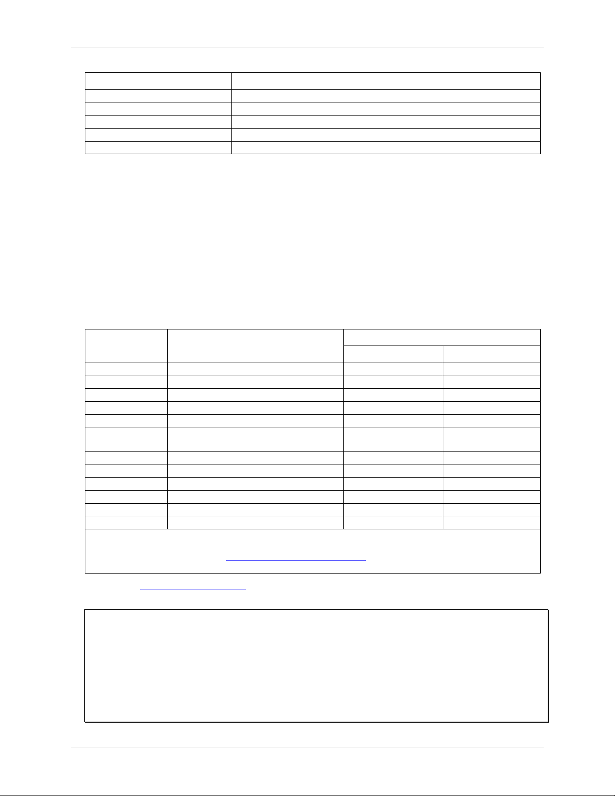
SC-1608 Series User's Guide About this User's Guide
Callout
Designation
Description
Default Configuration
1
SW1 (POWER)
Power switch
Off 2 SW2
8-position DIP switch for SSR module direction
All OUTPUT
3
W1
Non-invert/Invert logic control jumper
INVERT
4
SSR0 to SSR7
Mounting locations for SSR digital I/O modules
Unpopulated
5
CH0 to CH7
Mounting locations for 8B input modules
Unpopulated
6
J30
AOUT0 voltage divider for module location CH8 (U9)
±10 V
7
J29
AOUT0 readback or convert location CH8 (U9) to input
OUT (no function)
8
J32
AOUT1 voltage divider for module location CH9 (U10)
±10 V
9
J31
AOUT1 readback or convert location CH9 (U10) to input
OUT (no function)
10
CH8 to CH9
Mounting locations for 8B I/O modules (analog voltage input or
voltage/current output)
Unpopulated
11
J21 to J28
CJC Enable jumpers
All Disabled
12
R1 to R8
Resistor locations
Unpopulated
Default configuration
Each SC-1608 Series product has switches and jumpers on the baseboard that should be configured before use.
Refer to Figure 1 and the table below list the location and default setting of each configurable item. Refer to the
Functional Details chapter on page 14 for more information about each item.
Figure 1. Configurable component locations
6
Page 7

SC-1608 Series Product
Components
SC-1608-2AO-ENET
SCC-8-8-2 baseboard and power supply, E-1608-OEM, cable, accessory kit
SC-1608X-2AO-USB
SCC-8-8-2 baseboard and power supply, USB-1608GX-2AO-OEM, cable, accessory kit
SC-1608X-USB
SCC-8-8-2 baseboard and power supply, USB-1608GX-OEM, cable, accessory kit
SC-1608-USB
SCC-8-8-2 baseboard and power supply, USB-1608G-OEM, cable, accessory kit
Chapter 1
Introducing the SC-1608 Series
The SC-1608 Series is a family of products that integrate DAQ functionality, isolated analog signal
conditioning, and isolated digital I/O signal conditioning on one board. The SC-1608 Series includes the
following products:
You can install industry-standard 8B analog signal conditioning modules and solid state relay (SSR) digital I/O
modules onto the baseboard. The SC-1608 Series can be installed in a rack mount enclosure or used on a bench.
SCC-8-8-2 baseboard
The SCC-8-8-2 baseboard provides the following features:
Connectors for mating with a USB-1608G-OEM Series board or E-1608-OEM board.
Mounting locations for eight 8B analog input modules and two 8B analog input or output modules.
8B modules provide 500 V channel-to-channel isolated signal conditioning for voltage, thermocouples,
RTD, strain gauge, current and frequency type signals.
Mounting locations for eight SSR digital I/O modules.
o SSR digital I/O modules are isolated relay control modules that sense AC/DC voltages from a field
source and respond with a digital output signal, or to switch and control AC/DC loads using a digital
signal. You set the module type for input or output, and the logic polarity to invert or non-invert.
50-pin User I/O header connector.
o The 50-pin User I/O header connector is where all non-conditioned input and output signals are
available for user connections.
Screw terminals to access all conditioned analog and digital signals.
The SCC-8-8-2 baseboard is powered with a supplied 12 volt, 30 watt external power supply. An alternate
power header is available to connect a user-supplied 12 VDC power supply.
Integrated DAQ Functionality
The USB-1608G-OEM Series board or E-1608-OEM mates directly onto the SCC-8-8-2 baseboard.
Unless a feature is applicable only to a specific SC-1608 Series product, this document refers to the USB-
1608G-OEM Series and E-1608-OEM board as OEM DAQ board.
USB-1608G-OEM Series
The USB-1608G-OEM Series includes the USB-1608GX-2AO-OEM, USB-1608GX-OEM, and
USB-1608G-OEM. These boards provide the following features:
Eight differential (DIFF) or 16 single-ended (SE) analog input channels (SE mode is required for use with
8B analog I/O modules)
Sample rates up to 500 kS/s aggregate
Two analog output channels (USB-1608GX-2AO-OEM)
Eight individually-configurable digital I/O channels
Two counter channels (32-bit) that count TTL pulses
One timer output channel (32-bit)
Header connectors for mating with the SCC-8-8-2 baseboard
7
Page 8

SC-1608 Series User's Guide Introducing the SC-1608 Series
OEM Hardware manuals
Refer to the hardware manual for each USB-1608G-OEM Series board for more information about the DAQ
features.
USB-1608GX-2AO-OEM: www.mccdaq.com/PDFs/manuals/USB-1608GX-2AO-OEM.pdf
USB-1608GX-OEM: www.mccdaq.com/PDFs/manuals/USB-1608GX-OEM.pdf
USB-1608G-OEM: www.mccdaq.com/PDFs/manuals/USB-1608G-OEM.pdf
E-1608G-OEM
The E-1608-OEM provides the following features:
Four differential (DIFF) or eight single-ended (SE) analog input channels (SE mode is required for use with
8B analog I/O modules)
Sample rates up to 250 kS/s aggregate
Two analog output channels (16-bit)
Eight individually-configurable digital I/O channels
One counter channel (32-bit) that counts TTL pulses
Header connectors for mating with the SCC-8-8-2 baseboard
Hardware manual
Refer to the E-1608-OEM hardware manual at www.mccdaq.com/PDFs/manuals/E-1608-OEM.pdf for more
information about its DAQ features
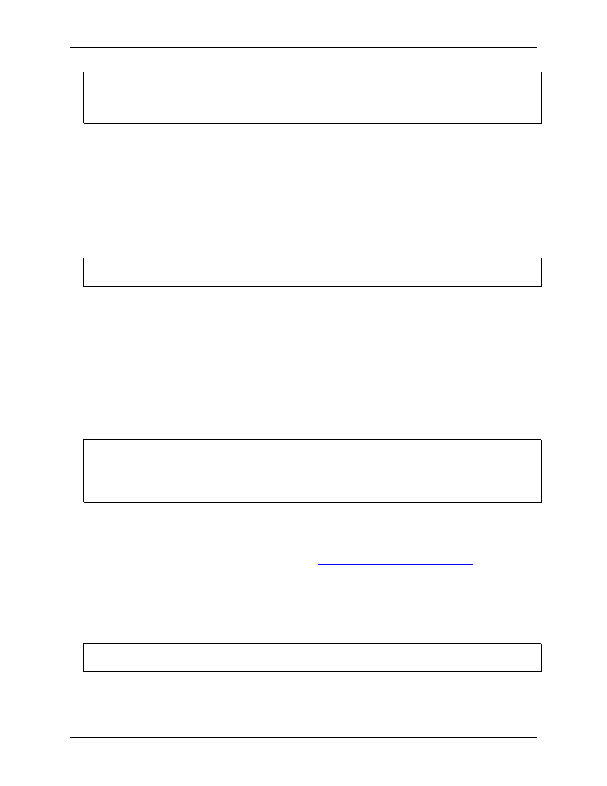
Functional block diagrams
SC-1608X-2AO-USB
Figure 2 shows the functionality provided by a SC-1608X-2AO-USB with analog I/O 8B modules and digital
I/O SSR modules installed. The SC-1608X-USB and SC-1608-USB provide the same functionality without the
analog output capability.
Figure 2. SC-1608X-2AO-USB functionality
The USB-1608G-OEM Series devices receive power from the +5 V USB supply from your computer.
8
Page 9

SC-1608 Series User's Guide Introducing the SC-1608 Series
SSR module type
Description
SSR-IAC-05
AC sense, 90 to 140 VAC/VDC
SSR-IAC-05A
AC sense, 180 to 280 VAC/VDC
SSR-IDC-05
DC sense, 3 to 32 VDC
SC-1608-2AO-ENET
Figure 3 shows the functionality provided by a SC-1608-2AO-ENET with analog I/O 8B modules and digital
I/O SSR modules installed.
Figure 3. SC-1608-2AO-ENET functionality
The E-1608-OEM receives power from the included external supply when the baseboard is powered on. When
connected to the baseboard, the E-1608-OEM power header connector (W1 on the OEM DAQ board) mates
with the +5 V power header connector (J37) on the baseboard. No additional supply is required.
Compatible modules
When using the SC-1608X-2AO-USB, SC-1608X-USB, SC-1608-USB, the total current available for 8B
analog I/O modules and SSR digital I/O modules is 1612 mA, maximum. When using the SC-1608-2AOENET, the total current available for 8B analog I/O modules and SSR digital I/O modules is 1292 mA,
maximum. Keep these values in mind when installing modules.
SSR digital I/O control modules
SSR digital I/O modules are solid state relay control modules that provide 4000 Vrms optical isolation. Digital
input modules sense AC/DC voltages from field devices and convert them to digital TTL signals. Digital output
modules use TTL signals to switch and control AC/DC loads.
The baseboard has eight locations for single channel solid state relay modules. The input/output type is
configured with onboard switch SW2. The polarity is configured with onboard jumper W1. The table below lists
the input and output modules that you can install.
SSR digital I/O modules compatible with the SC-1608 Series
9
Page 10
SC-1608 Series User's Guide Introducing the SC-1608 Series
SSR module type
Description
SSR-IDC-05NP
DC sense, 10 to 32 VDC non-polarized digital inputs
SSR-OAC-05
AC switch, 24 to 140 VAC, 3.5 A @ 120 VAC
SSR-OAC-05A
AC switch, 24 to 280 VAC, 3.5 A @ 240 VAC
SSR-ODC-05
DC switch, 1 to 60 VDC @ 3.5 A
SSR-ODC-05A
DC switch, 4 to 200 VDC @ 3.5 A
8B module type
Measurement type
Max number of supported modules*
Ethernet version
USB version
8B30/31
Voltage input, 3 Hz bandwidth
8
8 or 10*
8B32
Current input, 0-20 mA, 4-20 mA
8
8 or 10*
8B33
Isolated true RMS input
8
8 or 10*
8B34
Linearized 2- or 3-wire RTD input
8
8
8B35
Linearized 4-wire RTD input
8
8
8B38
Strain gage input, 8 kHz and 3Hz bandwidth
7 with no SSRs installed
6 with SSRs installed
8
8B39-01
Current output, 0-20 mA, 4-20 mA
2
2
8B40/41
Voltage input, 1 kHz bandwidth
8
8 or 10*
8B45
Frequency input
8
8
8B47J/K/T
Linearized thermocouple input
8
8
8B49
Voltage output 2 2
8B50/51
Voltage input, 20 kHz bandwidth
8
8 or 10*
* When using the SC-1608X-USB or SC-1608-USB, you can install two additional 8B voltage input modules into the 8B
I/O module locations (for a total of 10). Voltage input modules installed in the I/O location must be 2-wire types that don't
require excitation terminals. Refer to 8B analog I/O module control jumpers on page 19 for details. The SC-1608-2AOENET or SC-1608X-2AO-USB accept output modules in the two 8B I/O module locations only.
8B analog I/O signal conditioning modules
8B analog modules provide 500 V channel-to-channel isolated analog I/O signal conditioning. Mix and match
per channel between supported voltage, TC, RTD, strain gage, current, and frequency type signals.
8B analog input modules isolate, filter, and amplify an input signal and provide an analog voltage output.
8B analog output modules accept an input signal from a non-isolated source, then isolate, filter, and convert
the signal to a voltage or current output.
The baseboard has eight locations for 8B analog input modules, and two locations for 8B analog input or analog
output modules.
The following table lists the 8B analog I/O module types you can install, and the maximum number of each
module that can be installed:
8B analog I/O modules compatible with the SC-1608 Series
Refer to the MCC Signal Conditioning page on our website for a list of the specific modules supported within
each module type.
OEM DAQ Analog Ranges
The analog input range of the OEM DAQ boards can be configured for ±5 V which allows them to interface to
most of the 8B output modules. The resolution and accuracy of the OEM DAQ boards is sufficient for use with
8B output modules that have a unipolar 0-5 V output range.
The analog output voltage range of the SC-1608-2AO-ENET and SC-1608X-2AO-USB is ±10 V, allowing the
baseboard to interface with many of the 8B modules. For 8B modules with a ±5 V or unipolar 0-5 V range, you
can scale the ±10 V outputs to ±5 V, so that combined with the resolution and accuracy of the OEM DAQ
boards these modules are also supported.
10
Page 11

Installing the SC-1608 Series
SC-1608 Series products ship as the following components:
OEM DAQ board (USB-1608G-OEM Series or E-1608-OEM)
SCC-8-8-2 baseboard (pre-assembled with standoffs)
External 12 VDC power supply (MCC p/n PS-12V30WEPS)
USB and Ethernet cables; use the cable specific to your DAQ board.
Accessory kit – contains standoffs for securing the OEM DAQ board to the SCC-8-8-2 baseboard, a
protective shield that mounts onto the OEM DAQ board, and printed assembly instructions.
Unpacking
As with any electronic device, you should take care while handling to avoid damage from static
electricity. Before removing a board from its packaging, ground yourself using a wrist strap or by simply
touching the computer chassis or other grounded object to eliminate any stored static charge.
Contact us immediately if any components are missing or damaged.
Downloading the software
Chapter 2
Refer to the product page specific to your OEM DAQ board on the Measurement Computing website for
information about the supported software you can download.
Install the software before you connect the hardware to the computer
The driver needed to run the board is installed when you install the software. Therefore, you need to install the
software package you plan to use before you connect the OEM DAQ board.
Assembling the hardware
Perform the procedure below before connecting an OEM DAQ board to the baseboard:
1. Set the baseboard power switch (SW1) to OFF, and set each of the digital module I/O type DIP switch
positions (SW2) to match the specific module type that will be installed.
Both the OEM DAQ board and baseboard should be powered off while they are being assembled together.
2. Attach the hardware standoffs and protective shield to the OEM DAQ board.
Refer to the printed SC-1608 Series assembly instructions included in the shipment for the steps to perform
this procedure.
3. Configure the digital pull-up/down jumper on the OEM DAQ board for pull-down.
o E-1608-OEM: Set jumper W3 for pull-down; this setting is labeled PULL DN on the board.
o USB-1608 USB-1608G-OEM Series boards: verify jumper W1 is set for pull-down (shown below);
this is the default setting.
4. Mate the OEM DAQ board you are using with the baseboard; perform the step specific to your OEM DAQ
board:
o USB-1608G-OEM Series: plug the board into socket connectors J5 and J6 (labeled USB-1608G-OEM
Series ONLY on the baseboard). These connectors are polarized to ensure the proper orientation when
mating the boards together. Refer to the "Cable Entry" board label for proper orientation.
o E-1608-OEM: plug the board into socket connectors J3 and J4 (labeled E-1608-OEM ONLY on the
baseboard). These connectors are not polarized, so take care to properly orient the board. Refer to the
Cable Entry board label for proper orientation.
11
Page 12
SC-1608 Series User's Guide Installing the SC-1608 Series
Verify that the OEM DAQ board is properly connected
Ensure that the header pins on the OEM DAQ board are properly connected to the OEM header connectors on
the baseboard. Orient the OEM DAQ board so the USB/Ethernet cables connect to the OEM DAQ board at the
left edge of the baseboard. Refer to the Cable Entry board label for proper orientation.
5. Attach the supplied PC interface cable to the OEM DAQ board; perform one of the following steps:
o Attach the USB cable to a USB-1608G-OEM Series board and the computer or self-powered hub.
o Attach the CAT-6 Ethernet cable to the E-1608-OEM board.
Installing 8B analog I/O modules
You can install up to eight 8B analog input modules into the baseboard mounting locations labeled CH0 to CH7,
and two analog input or analog output modules into mounting locations labeled CH8 and CH9. When using a
product with analog outputs you must install an output module in CH8/CH9. When using a product without
analog outputs you can install a voltage input module into CH8/CH9.
Power down the baseboard whenever you install or remove 8B analog I/O modules
Make sure the power switch SW1 is OFF before you install or remove 8B modules.
Each 8B analog input module (CH0 to CH7) has dedicated positive (+) and negative (–) inputs, along with
positive (+) and negative (–) excitation inputs. Each 8B output module has dedicated positive (+) and negative
(–) outputs. All signals are brought out to screw terminals for field wiring connections. When using CH8 and
CH9 with 8B input modules installed, note that there are no associated ± excitation pins.
Perform the following steps to install 8B analog I/O modules:
1. Turn the baseboard power switch SW1 OFF.
2. Align the 8B module retaining screw and pins with the holes on the circuit board.
3. Gently press the module into place.
4. Tighten the retaining screw; do not over-tighten.
5. Repeat these steps to install additional 8B analog I/O modules.
Configuring for ten 8B analog input modules
8B analog I/O mounting locations CH8 and CH9 are configured by default for output. When connected to a
board without analog output functionality, such as the USB-1608G-OEM or USB-1608GX-OEM, these
locations can be converted to 8B analog input modules via onboard jumpers. Refer to 8B analog I/O module
control jumpers on page 19 for more information.
Configuring 8B analog I/O modules
Onboard jumpers let you enable CJC for thermocouple input modules, convert the analog output module
locations to input, and scale the OEM DAQ analog output channel voltage to ±5V to match the voltage range
output by an installed 8B analog output module. Refer to 8B analog I/O module control jumpers on page 19 for
details about how to use the 8B module control jumpers.
Installing SSR digital I/O modules
You can install up to eight digital I/O modules into the mounting locations labeled SSR0 to SSR7. Each
location can be set for either input or output with the DIP switch labeled SW2.
Power down the baseboard whenever you install or remove a digital I/O module
Make sure the power switch SW1 is OFF before you install or remove an SSR module.
Mounting screw threads are provided to easily install the SSR modules. SSR modules use a standard color
scheme so you can quickly identify what module type is installed. Positive (+) and negative (–) relay contacts
are brought out to screw terminals for field wiring connections. Each SSR module has an associated LED that
turns on when the module output state is active.
12
Page 13
SC-1608 Series User's Guide Installing the SC-1608 Series
Perform the following steps to install SSR digital I/O modules:
1. Turn the baseboard power switch SW1 OFF.
2. Align the SSR module retaining screw and pins with the holes on the circuit board.
3. Gently press the module into place.
4. Tighten the retaining screw; do not over-tighten.
5. Repeat these steps to install additional SSR modules.
6. Configure the SW2 DIP switch to match the input/output type for each installed module.
Configuring the OEM DAQ boards with software
Before using a SCC-8-8-2 product, configure the analog input mode on the OEM DAQ board. When using the
SC-1608-2AO-ENET, the E-1608-OEM network settings must also be configured.
Perform the following steps to configure the OEM DAQ board for use with the SCC-8-8-2:
Configure the analog input mode with software for single-ended mode.
Configure network settings (SC-1608-2AO-ENET only). Refer to the E-1608-OEM manual at
www.mccdaq.com/PDFs/manuals/E-1608-OEM.pdf for details about network settings.
Powering up
To prevent digital inputs from floating, do not apply power to the baseboard before connecting to the OEM
DAQ board.
The E-1608-OEM receives power from the baseboard when the boards are connected. The USB-1608G-OEM
Series board is powered from the USB connector on a computer or self-powered hub. The digital channels on
the USB-1608G-OEM Series OEM DAQ board and the SCC-8-8-2 power up in digital input mode, so neither
board can drive current into the other when powered on. Therefore, the power up sequence of the two boards is
arbitrary; either board can be powered on first.
Perform the following steps to power up an SCC-8-8-2 product:
1. USB-1608G-OEM Series: connect the USB cable into the USB connector on the computer or self-powered
hub.
The E-1608-OEM doesn't require a separate power supply, as the board receives power from the SCC-8-8-
2 baseboard when connected.
2. Connect a power supply to the SCC-8-8-2 baseboard; perform one of the following steps:
o Connect the supplied 12 VDC external power supply to connector J1.
o Connect a 12 VDC 2.5 A power supply (not supplied) to the 2-pole terminal block at J2.
A higher-amperage supply may be used. The SC-1608 Series is designed with over current protection
that prevents board damage if the current drawn exceeds 2 A.
Connect a 12 VDC supply to either connector J1 or J2
Do not attempt to apply power to both external power connectors simultaneously.
3. Turn the baseboard power switch SW1 On.
Avoiding logic contention
Pay careful attention to the DIO configuration of the baseboard digital pins (set with SW2) and the OEM DAQ
board in order to avoid a logic contention issue. You configure the OEM DAQ board with software.
13
Page 14

1
External power connectors J1 and J2
10
8B I/O module control jumpers J29 and J30 (for CH8)
J29: AOUT0 readback or convert to input module location
J30: AOUT0 voltage divider
2
E-1608-OEM connectors J3, J4, and J37
11
8B I/O module control jumpers J31 and J32 (for CH9)
J31: AOUT1 readback or convert to input module location
J32: AOUT1 voltage divider
3
8-position DIP switch for SSR module direction
12
8B I/O module mounting locations CH8 and CH9
4
Non-invert/Invert logic control jumper W1
13
CJC Enable jumpers J21 to J28
5
USB-1608G-OEM Series connectors J5to J6
14
R1 - R8 resistor locations
6
SSR I/O module mounting locations SSR0 to SSR7
15
8B module screw terminals
7
SSR I/O module status LEDs (8)
16
SSR I/O module screw terminals
8
User I/O header connector J35
17
Power switch SW1
9
8B input module mounting locations CH0 to CH7
Chapter 3
Functional Details
This chapter discusses the functional details of the SCC-8-8-2 baseboard. For functional details of the OEM
DAQ board, refer to the hardware manual specific to the SC-1608 Series;
USB-1608GX-2AO-OEM: www.mccdaq.com/PDFs/manuals/USB-1608GX-2AO-OEM.pdf
USB-1608GX-OEM: www.mccdaq.com/PDFs/manuals/USB-1608GX-OEM.pdf
USB-1608G-OEM: www.mccdaq.com/PDFs/manuals/USB-1608G-OEM.pdf
E-1608-OEM: www.mccdaq.com/PDFs/manuals/E-1608-OEM.pdf
SCC-8-8-2 baseboard components
The location of each component on the baseboard is shown in Figure 4.
Figure 4. SCC-8-8-2 baseboard components
External power connectors
External power can be connected to either power connector J1 (barrel connector) or J2 (terminal block). Do not
attempt to apply power to both power connectors simultaneously.
Connector J1 connects to the +12 VDC external power supply included in the SCC-8-8-2 shipment.
Connector J2 connects to a user-supplied +12 VDC power supply.
Figure 5 shows a schematic for external power connectors J1 and J2.
14
Page 15

SC-1608 Series User's Guide Functional Details
Figure 5. J1 and J2 power schematic
Power switch
SW1 is the main power switch that provides power to the baseboard when it is switched on and when an
external supply is connected to either J1 or J2.
E-1608-OEM connectors
Socket connectors J3 and J4 connect with the header connectors on an E-1608-OEM board.
The J37 header connector is used to power the E-1608-OEM. When the E-1608-OEM connects to the
baseboard, its power input header (W1) mates with the baseboard power header connector (J37).
The E-1608-OEM receives power from the SCC-8-8-2 baseboard
Do not connect an external supply to the E-1608-OEM barrel input connector.
Pinout tables for J3, J4, and J37 are listed in the Specifications chapter.
USB-1608G-OEM Series connectors
Socket connectors J5 and J6 connect with the header connectors on a USB-1608G-OEM Series board. The
connectors are keyed to ensure proper board orientation. Pinout tables for socket connectors J5 and J6 are listed
in the Specifications chapter.
50-pin User I/O header connector
J35 is a 50-pin header connector where all conditioned and non-conditioned input and output signals are
available for user connections.
The eight analog inputs, two analog outputs, and eight digital I/O that interface with the 8B analog I/O modules
and digital I/O modules are connected directly to this header connector. Any non-conditioned input or output
can be used as a non-isolated channel.
Do not connect to a signal being used by an analog or digital module
Be careful not to connect to a signal already in use by a digital I/O or analog I/O module.
15
Page 16

SC-1608 Series User's Guide Functional Details
Pin
Signal
name
Pin description
Pin
Signal
name
Pin description
1
CH0
Analog input 0 (single-ended)
2
CH1
Analog input 1 (single-ended)
3
CH2
Analog input 2 (single-ended)
4
CH3
Analog input 3 (single-ended)
5
GND
Ground
6
GND
Ground
7
CH4
Analog input 4 (single-ended)
8
CH5
Analog input 5 (single-ended)
9
CH6
Analog input 6 (single-ended)
10
CH7
Analog input 7 (single-ended)
11
GND
Ground
12
GND
Ground
13
CH8
Analog input 8 (single-ended)
14
CH9
Analog input 9 (single-ended)
15
CH10
Analog input 10 (single-ended)
16
CH11
Analog input 11 (single-ended)
17
GND
Ground
18
GND
Ground
19
CH12
Analog input 12 (single-ended)
20
CH13
Analog input 13 (single-ended)
21
CH14
Analog input 14 (single-ended)
22
CH15
Analog input 15 (single-ended)
23
GND
Ground
24
GND
Ground
25
AOUT0
Analog output 0
26
GND
Ground
27
AOUT1
Analog output 1
28
GND
Ground
29
+VO
+5V user output
30
GND
Ground
31
GND
Ground
32
GND
Ground
33
DIO0
DIO bit 0
34
DIO1
DIO bit 1
35
DIO2
DIO bit 2
36
DIO3
DIO bit 3
37
DIO4
DIO bit 4
38
DIO5
DIO bit 5
39
DIO6
DIO bit 6
40
DIO7
DIO bit 7
41
AICLKI
AI clock input
42
AICLKO
AI clock output
43
AOCLKI
AO clock input
44
AOCLKO
AO clock output
45
TRIG
Trigger Input
46
GND
Ground
47
CTR0
Counter 0 Input
48
CTR1
Counter 1 input
49
TMR
Timer Output
50
GND
Ground
The following table lists the pinout for header connector J35.
J35 connector pinout
Analog input signals CH8 to CH15 have no function when the E-1608-OEM is connected. Analog output
signals AOUT0 and AOUT1 and AOCLKO have no function when a USB-1608G-OEM or USB-1608GXOEM is connected.
Connector cabling and signal termination
The User I/O connector is compatible with C50FF-x ribbon cable and CIO-MINI50 screw terminal board.
Details on these accessories are available on our website.
SSR I/O module input/output type DIP switch
Switch SW2 is an 8-position DIP switch used to set the module type for each installed SSR module as either
input or output. Each DIP switch position is set by default for OUTPUT. Switch SW2 is shown in Figure 6.
Figure 6. I/O module type DIP switch SW2
Push down on the left side to set the DIP switch position for input; push down on the right side to set the DIP
switch position for output.
16
Page 17

SC-1608 Series User's Guide Functional Details
Pin
Signal name
Pin description
1
SSR0 +
Digital I/O module 0+
2
SSR0 –
Digital I/O module 0 –
3
SSR1 +
Digital I/O module 1+
4
SSR1 –
Digital I/O module 1 –
5
SSR2 +
Digital I/O module 2+
6
SSR2 –
Digital I/O module 2–
7
SSR3 +
Digital I/O module 3+
8
SSR3 –
Digital I/O module 3–
9
SSR4 +
Digital I/O module 4+
10
SSR4 –
Digital I/O module 4–
11
SSR5 +
Digital I/O module 5+
12
SSR5 –
Digital I/O module 5–
13
SSR6 +
Digital I/O module 6+
14
SSR6 –
Digital I/O module 6–
15
SSR7 +
Digital I/O module 7+
16
SSR7 –
Digital I/O module 7–
Set SW2 to INPUT for use with digital input modules. Set to OUTPUT for use with digital output modules.
You set the digital direction of the OEM DAQ board digital channels with software. SW2 switches have no
effect on the bit direction of the digital I/O channels on the OEM DAQ board.
When a switch position is set for output, the behavior of the associated digital module is affected by the
configuration of the invert logic jumper (W1 ) and the digital logic state of the OEM DAQ board. Module
behavior for each configuration is summarized in the Digital output logic control section on page 23.
Non-invert/Invert logic control jumper
Jumper W1 sets the control logic polarity for each digital output module installed in locations SSR0-SSR7 to
inverted logic (active high, default) or non-inverted (active low). Figure 7 shows W1 set for inverted logic.
Figure 7. Switch S2 default configuration
The invert/non-invert setting applies only to output modules, and has no effect on input modules. When a
switch position is set for output, the associated output module behavior is determined by the configuration of
the invert logic control jumper (W1) and the digital logic state set for the OEM DAQ board digital bits. The
logic table on page 23 summarizes module behavior for each configuration.
Digital I/O module mounting locations
You can install up to eight digital I/O modules into mounting locations SSR0 to SSR7. Supported modules are
listed on page 9. Set the module input/output type for each installed module with onboard switch SW2.
Digital I/O module LEDs
Each digital I/O module has an associated LED. For digital output modules, the LED turns on when the module
is active (turned on). For digital input modules, the LED turns on when the module detects an input voltage
(logic high).
Digital I/O module screw terminals
The SCC-8-8-2 has eight pairs of screw terminals for field wiring connections. Positive (+) and negative (–)
relay contacts are brought out to screw terminals SSRx+ and SSRx–.
Use 16 AWG to 30 AWG wire for your signal connections. Properly insulate and dress the wires to avoid any
short circuit to adjacent channels or other points on the board.
SSR digital I/O module pinout
17
Page 18

SC-1608 Series User's Guide Functional Details
J21-J28 Jumper Position
Function
1-2
CJC enabled
2-3
CJC disabled (default)
8B analog input module mounting locations
You can install up to eight 8B analog input modules into mounting locations CH0 to CH7. When using a
product without analog output capability, such as the SC-1608X-USB or SC-1608-USB, you can install a
voltage input module into locations CH8 or CH9, and convert the location to input using an onboard jumper.
Refer to 8B analog I/O module control jumpers on page 19 for more information about how to use the I/O
module jumpers.
CJC Enable jumpers
Use the CJC Enable jumpers J21 to J28 to enable cold-junction compensation for each 8B thermocouple input
module installed in 8B input module locations CH0 to CH7. Configure the jumper directly below the location
where the thermocouple module is installed.
The following table lists the configuration options for CJC Enable jumpers J21 to J28.
CJC Enable Jumpers J21-J28 configuration
Figure 8 shows a typical jumper configured to enable CJC.
Figure 8. CJC jumper configured to enable CJC
If you are not using thermocouple input modules, make sure that jumpers J21 to J28 are disabled (position 2-3).
8B analog I/O module mounting locations
8B I/O module locations CH8 and CH9 are wired for output. When using a product without analog output
capability, such as the SC-1608X-USB or SC-1608-USB, you can install a voltage input module in these
locations. Voltage input modules installed in CH8 and CH9 must be 2-wire types that don't require excitation
terminals. When using the SC-1608-2AO-ENET or SC-1608X-2AO-USB, you must install a voltage or current
output module.
Each I/O module location has an associated pair of jumpers that let you either convert the location to input, or
read back an output voltage at the header connector, depending on the type of module installed. You can also
scale the default analog output voltage to match the range of an installed 8B output module. Refer to the 8B
analog I/O module control jumpers section on page 19 for details about how to use the jumpers.
R1 to R8 resistor locations
You can install plug-in shunt resistors at locations R1 to R8 to monitor a 4-20 mA current loop, or to measure
current using 8B analog voltage input modules.
Complete the following steps to monitor a 4-20 mA current loop or to measure current:
1. Turn the baseboard power switch SW1 OFF.
2. Plug the shunt resistor into the plug-in location for the applicable voltage input module. DO NOT solder
the resistor in place.
Shunt resistors can only be used with 8B voltage input modules
Shunt resistors must be removed when using other types of input modules, including current input modules.
Voltage input modules used to monitor a 4-20 mA loop often use a 250 Ω precision resistor to develop a 1 VDC
to 5 VDC voltage drop.
18
Page 19

SC-1608 Series User's Guide Functional Details
J29/31
jumper
position
Function
1-2
(default)
No function
2-3
output module
installed in
CH8 (U9) or
CH9 (U10)
This configuration lets you measure (read back) the value of the analog output voltage at the
header connector.
J29: connects OEM DAQ board output channel AOUT0 to the OEM DAQ board input channel
CH8 (J35 pin 13), or converts 8B I/O module location CH8 (U9) to an 8B input module
location.
J31: connects OEM DAQ board output channel AOUT1 to the OEM DAQ board input channel
CH9 (J35 pin 14), or converts 8B I/O module location CH9 (U10) to an 8B input module
location.
Note: When using the SC-1608X-2AO-USB, you can read back the AOUTx voltage from the
CH8/CH9 pins on the J35 header. When using the SC-1608-2AO-ENET, you can read back the
AOUTx voltage from J35 pins 25 and 27 using a voltmeter or other DAQ board.
2-3
input module
installed in
CH8 (U9) or
CH9 (U10)
This configuration converts the default output module location to input.
J29: converts module location CH8 to an input location.
J31: converts module location CH9 to an input location.
Note: Voltage input modules installed in CH8 or CH9 must be 2-wire types that don’t require
excitation terminals.
Shunt resistors are user-supplied
If installing a shunt resistor, we recommend using a Dataforth SCM7BXR1 250 Ω current conversion resistor.
Contact Dataforth for the specification.
8B analog I/O module control jumpers
Jumpers J29 and J31 are associated with the module installed in location CH8 (U9). Jumpers J30 and J32 are
associated with the module installed in CH9 (U10). Module locations CH8 and CH9 are wired by default for
output.
J29 and J30 can be used to convert an output location to input (this requires a board without AOUT
functionality), or to measure the analog output voltage being applied to the output module's input pin.
J30 and J32 are voltage divider jumpers used to scale the analog output voltage to match the output voltage
range of the installed module. These jumpers require that an output module be installed, and have no effect
when an input module is installed.
Jumpers J29 and J31
The following table lists the configuration options for the 8B output control jumpers J29 and J31.
Jumper J29 (location CH8) and J31 (location CH9) configuration
Figure 9 shows jumper 29 and 31 set for its default configuration. This jumper has no function when set to the
default 1-2 position.
Figure 9. Jumper 29 and J31 default configuration (no function)
19
Page 20

SC-1608 Series User's Guide Functional Details
Figure 10 illustrates the connection flow when an output module is installed in module location CH8, and
jumper J29 is set for position 2-3.
Figure 10. J29 set for position 2-3 with an output module installed in CH8 (U9)
In this scenario, the value of the voltage output from OEM DAQ board channel AOUT0 can be read from OEM
DAQ analog input channel CH8 at J35 pin 13 when using the SC-1608X-2AO-USB. When using the SC1608X-2AO-USB, the OEM DAQ AOUT0 voltage can be read with a meter or other DAQ board at J35 pin 25
(AOUT0) .
When set to position 1-2 (not shown in the diagram), the same voltage readback functionality is available using
J35 pin 25 and non-isolated analog input CH8 (pin 13). The signal is non-isolated in this configuration, since
the AOUT0 signal is no longer connected to AIN CH8.
Figure 11 illustrates the connection flow when an input module is installed in module location CH8, and jumper
J29 is set for position 2-3.
Figure 11. J29 set for position 2-3 with an input module installed in CH8 (U9)
In this scenario, the value of the input module's output voltage can be read from J35 header pin 13 when using
the SC-1608X-2AO-USB. The output value can also be read from header pin 25 with a meter or other DAQ
board when using the SC-1608-2AO-ENET or SC-1608X-2AO-USB.
20
Page 21

SC-1608 Series User's Guide Functional Details
J30/32
jumper
position
Function
1-2
(default)
J30: OEM DAQ board channel AOUT0 outputs ±10V output (default)
J32: OEM DAQ board channel AOUT1 outputs ±10V output (default)
2-3
J30: OEM DAQ board channel AOUT0 ±10V output is scaled to ±5V
OEM DAQ board channel AOUT1 ±10V output is scaled to ±5V
When set to position 1-2 (not shown in the diagram), the same voltage readback functionality is available using
J35 pin 25 and non-isolated analog input CH8 (pin 13). The signal is non-isolated in this configuration, as
AOUT0 is no longer connected to AIN CH8.
Voltage divider jumpers J30 and J32
These jumpers are used to scale the OEM DAQ board AOUTx channel output voltage range to match the
voltage input range of an analog output module installed at CH8 (U9) or CH9 (U10).
The following tables list the configuration settings of jumpers J30 and J32.
Jumper J30 (location CH8) and J32 (location CH9) configuration
Figure 12 shows jumper 30 and 32 set for its default configuration.
Figure 12. Jumper J30 and J32 default configuration (output ±10V)
Figure 13 illustrates the connection flow when an output module is installed in module location CH8, and
jumper J30 is set for position 2-3.
Figure 13. J30/J32 voltage divider schematic
In this scenario, the OEM DAQ board channel AOUT0 is configured to output ±10V.
If an 8B output module is installed that has an output range of ±5V or 0-5 V, configure this jumper for position
2-3 to scale the voltage output by the OEM DAQ board AOUT0 channel to ±5V.
21
Page 22

SC-1608 Series User's Guide Functional Details
Signal name
Pin description
CH0+
8B input module CH0+
CH0–
8B input module CH0–
EXC0+
8B input module excitation CH0+
EXC0–
8B input module excitation CH0–
CH1+
8B input module CH1+
CH1–
8B input module CH1–
EXC1+
8B input module excitation CH1+
EXC1–
8B input module excitation CH1–
CH2+
8B input module CH2+
CH2–
8B input module CH2–
EXC2+
8B input module excitation CH2+
EXC2–
8B input module excitation CH2–
CH3+
8B input module CH3+
CH3–
8B input module CH3–
EXC3+
8B input module excitation CH3+
EXC3–
8B input module excitation CH3–
CH4+
8B input module CH4+
CH4–
8B input module CH4–
EXC4+
8B input module excitation CH4+
EXC4–
8B input module excitation CH4–
CH5+
8B input module CH5+
CH5–
8B input module CH5–
EXC5+
8B input module excitation CH5+
EXC5–
8B input module excitation CH5–
CH6+
8B input module CH6+
CH6–
8B input module CH6–
EXC6+
8B input module excitation CH6+
EXC6–
8B input module excitation CH6–
CH7+
8B input module CH7+
CH7–
8B input module CH7–
EXC7+
8B input module excitation CH7+
EXC7–
8B input module excitation CH7–
CH8+
8B I/O module CH8+
CH8–
8B I/O module CH8–
CH9+
8B I/O module CH9+
CH9–
8B I/O module CH9–
8B analog I/O module screw terminals
Connect 8B analog input module signals to screw terminals labeled CH0+/CH0– to CH7+/CH7– and the
associated excitation terminals EXCx+/EXCx–. Connect 8B analog output module signals to CH8+/CH9+ and
CH8–/CH9–. Use 16 AWG to 30 AWG wire when connecting signals.
8B module screw terminals
Note that excitation terminals are provided only for analog input modules installed in CH0 to CH7, and are not
provided for locations CH8 or CH9, even if a voltage input module is installed.
22
Page 23

SC-1608 Series User's Guide Functional Details
Digital Output Logic State
SW2 Position
W1 Position
Digital Output Module
Logic 0
Output
Invert
Off
Logic 1
Output
Invert
On
Logic 0
Output
Non-Invert
On *
Logic 1
Output
Non-Invert
Off
* With this configuration, the SSR modules will turn On if the DAQ OEM device loses power. This scenario does not
normally occur because the SCC-8-8-2 is configured by default for inverting logic.
Mechanical drawing
Figure 14. SCC-8-8-2 baseboard mechanical dimensions
Digital output logic control
The behavior of a digital output module is determined by the configuration of SW2, invert logic jumper W1,
and the output logic state set on the OEM DAQ board.
The table below defines how a digital output module behave according to the configuration of the digital output
logic state, the position of SW2 switches, and the setting of invert logic control jumper W1.
Logic table
Signal connections
Analog input
Analog input signals CH0 to CH7 are mapped to both the User I/O connector and to 8B analog input locations
CH0 to CH7.
Analog input channels CH8 to CH15 on USB-1608G-OEM Series boards are mapped to the User I/O header
connector only. These signals are not present on the E-1608-OEM board.
Analog output
E-1608-OEM and SC-1608X-2AO-USB channels AOUT0 and AOUT1 are mapped to 8B module locations
CH8 and CH9 and to the header connector.
Locations CH8 and CH9 are wired for output by default.
Use jumpers J29/32 to convert the CH8/CH9 module location to input.
Use jumpers J30/32 to scale the analog output voltage from the default ±10 V to ±5 V.
Refer to 8B analog I/O module control jumpers on page 19 for information about the settings for each jumper.
23
Page 24

SC-1608 Series User's Guide Functional Details
Digital I/O
Digital channels DIO0 to DIO7 are mapped to SSR digital module locations SSR0 to SSR7 and to the header
connector.
The eight digital channels are bidirectional and bit-configurable as input or output. Use the SW2 DIP switch
positions to set the input or output type for each bit. The factory setting for each switch position is OUTPUT.
Use the invert logic control jumper W1 to set the control logic polarity for output modules. Input modules
operate as inverted regardless of the jumper setting.
Trigger, counter, and timer channels
The trigger, counter, and timer signals are available on the 50-pin User I/O header connector.
Mounting options
The SC-1608 Series can be used on a bench or installed in the ENC-19X5X5 rack mount enclosure available
from MCC.
24
Page 25
Parameter
Specification
8B analog input module CJC
sensor
(Note 1)
Vishay-Dale TFPT1206L1002DM
CJC control jumper J21-J28:
Position 1-2: CJC enabled
Position 2-3: CJC disabled (default)
Parameter
Specification
8B I/O module analog output
jumper control (J29 and J31)
(Note 2)
J29 position 1-2: No function (default)
J29 position 2-3: Connects DAQ AOUT0 to DAQ analog input CH8 (J35 pin 13), or
converts 8B I/O location CH8 to an 8B input module location.
J31 position 1-2: No function (default)
J31 position 2-3: Connects DAQ AOUT1 to DAQ analog input CH9 (J35 pin 14), or
converts 8B I/O location CH9 to an 8B input module location.
8B I/O module voltage divider
jumper control (J30 and J32)
(Note 3)
2×4.99 kΩ resistor, 0.1% tolerance, 25 ppm
J30 position 1-2: DAQ AOUT0 outputs ±10 V output range (default)
J30 position 2-3: DAQ AOUT0 outputs ±5 V output range
J32 position 1-2: DAQ AOUT1 outputs ±10V output range (default)
J32 position 2-3: DAQ AOUT1 outputs ±5V output range
Chapter 4
Specifications
This chapter lists specifications for the SCC-8-8-2 baseboard
The specifications in this chapter are specific to the SCC-8-8-2 baseboard. Refer to the OEM user's guide or
SC-1608 Series data sheet posted on our website for OEM DAQ board specifications.
All specifications are subject to change without notice.
Typical for 25 °C unless otherwise specified.
Specifications in italic text are guaranteed by design.
Analog input
Table 1. Analog input CJC specifications
Note 1: Each 8B analog input module location (CH0-CH7) includes a CJC sensor and three-pin header with
jumper control (J21-J28).
Analog output
Table 2. Analog output jumper control specifications
Note 2: Three-pin headers J29 and J31 can be configured to read the OEM DAQ board's analog output
control voltage at 8B I/O module locations with OEM DAQ board AIN CH8 and CH9 when using
the USB-1608GX-2AO-OEM. When using the E-1608-OEM, the AOUTx voltage can be read at the
J35 header connector (pins 25 and pins 27) using a voltmeter or other DAQ board.
When using a DAQ board that does not have analog output capability, such as the USB-1608GOEM and USB-1608GX-OEM, configuring headers J29 and J31 for position 2-3 converts 8B I/O
module locations CH8 and CH9 to an 8B input module location (for a total of 10 8B input locations).
Voltage input modules installed in CH8 and CH9 must be 2-wire types that don't require excitation
terminals.
25
Page 26

SC-1608 Series User's Guide Specifications
Parameter
Specification
Number of I/O control logic
8
SSR default configuration
(Note 4)
OUTPUT type (SW2 default)
Configuration
Each module location (SSR0–SSR7) is individually configurable as INPUT or OUTPUT
using switch SW2.
Logic inversion control
(Note 5)
Configurable for inverting or non-inverting logic with jumper W1; set by default to
INVERT.
LED
Each module location (SSR0-SSR7) has a dedicated LED for indicating the module
status.
Parameter
Specification
Digital type
5V TTL
Number of I/O
8
Configuration
Bidirectional: each bit is individually configurable as digital input or digital output using
DIP switch SW2 (Note 6).
Connector location
J35
Input high voltage threshold
2.0 V min
Input high voltage limit
5.5 V absolute max
Input low voltage threshold
0.8 V max
Input low voltage limit
–0.5 V absolute min
0 V recommended min
Output high voltage
4.4 V min (IOH = –50 µA)
3.76 V min (IOH = –24 mA)
Output low voltage
0.1 V max (IOL = 50 µA)
0.44 V max (IOL = 24 mA)
Power On default state
Digital output, +5V logic level
Note 3: The voltage divider jumper options let you scale the OEM ±10V AOUTx to a ±5V output. To make
this change, place either of the J30 (CH8) and J32 (CH9) jumpers in the 2-3 position.
SSR module I/O control
Table 3. SSR module specifications
Note 4: Set the SW2 DIP switch to INPUT for use with SSR input modules such as the Grayhill 70IDC5.
The OEM DAQ board should be configured for digital input mode.
Set the SW2 DIP switch to OUTPUT for use with SSR output modules such as the Grayhill
70ODC5. The OEM DAQ board should be configured for digital output mode.
Note 5: The inverting logic feature is applied to SSR digital output modules only. The setting of jumper W1
has no effect on SSR digital input modules.
Digital input/output
Table 4. Digital input/output specifications
Note 6: Take care to avoid creating a digital I/O logic contention state between the DAQ board DIO and the
SCC-8-8-2 DIO.
26
Page 27

SC-1608 Series User's Guide Specifications
Parameter
Condition
Specification
External power input
connectors (Note 7)
J1: barrel type
J2: 2-pole terminal block, (16 AWG to 30 AWG)
External power input voltage
range (Note 8)
12V, ±5%
External power supply current
25 mA typical (Note 9)
1700 mA max, including all external loading
External power supply
(included)
MCC p/n PS-12V30WEPS
+12 V DC, 30 Watt, 5% regulation
+VO output voltage range
User I/O connector J35, pin 29
4.50 V min to 5.25 V max
+VO output current
10 mA max
Power LED
3V < V
ext
< 15 V: LED is ON
V
ext
> 15 V: LED OFF (power fault)
Power ON sequence (Note 10)
Arbitrary; either the SCC-8-8-2 or the OEM DAQ
board can be powered on first.
Power
Table 5. Power specifications
Note 7: The SCC-8-8-2 can be powered from either of the external power connectors J1 or J2. Do not
attempt to apply power to both external power connectors simultaneously.
Note 8: This specification applies to the actual voltage level present at the input to the external power
connector (J1 or J2) of the SCC-8-8-2, as any significant loading of the external power supply will
cause a voltage drop across the power supply cable.
Note 9: This is the total quiescent current requirement for the device, and does not include any potential
loading of the 8B modules, SSR modules, digital I/O bits, or +VO terminal.
Note 10: To prevent digital inputs from floating, both the SCC-8-8-2 and the OEM DAQ board should be
powered off while they are being assembled together.
Note 11: When using a USB-1608G-OEM-Series board, the total current available for 8B analog I/O modules
and SSR digital I/O modules is 1612 mA, maximum.
When using the E-1608-OEM, the total current available for 8B analog I/O modules and SSR digital
I/O modules is 1292 mA, maximum. For example, this current limitation would restrict the number
of 8B38 strain gage modules that can be installed on the SC-1608-2AO-ENET to six (when SSR
modules are installed), or seven (when no SSR modules are installed). Refer to the SC-1608 Series
User's Guide for details.
27
Page 28
SC-1608 Series User's Guide Specifications
Parameter
Specification
Operating temperature range
0 °C to 50 °C max
Storage temperature range
–40 °C to 85 °C max
Humidity
0% to 90% non-condensing max
Parameter
Condition
Specification
Dimensions (L × W × H)
SCC-8-8-2 with 0.38 in. standoffs
SCC-8-8-2 with 0.38 in. standoffs, OEM,
and protective shield
Note 12
101.6 × 426.72 × 42.16 mm
(4.0 × 16.8 × 1.66 in)
SCC-8-8-2 with SSR modules installed
(SSR modules sold separately)
101.6 × 426.72 × 48.50 mm
(4.0 × 16.8 × 1.91 in)
Parameter
Specification
Connector type
Screw terminal
Wire gauge range
16 AWG to 30 AWG
Environmental
Table 6. Environmental specifications
Mechanical
Table 7. Mechanical specifications
Note 12: The height of the SCC-8-8-2 User I/O connector is the same height as the SCC-8-8-2 assembled with
the OEM and protective shield, so these dimensions apply to the SCC-8-8-2 alone as well as
assembled with an OEM and shield.
Screw terminal connectors
Table 8. Screw terminal connector specifications
28
Page 29

SC-1608 Series User's Guide Specifications
Pin
Signal name
Pin description
1
SSR0 +
SSR I/O module 0+
2
SSR0 –
SSR I/O module 0 –
3
SSR1 +
SSR I/O module 1+
4
SSR1 –
SSR I/O module 1 –
5
SSR2 +
SSR I/O module 2+
6
SSR2 –
SSR I/O module 2–
7
SSR3 +
SSR I/O module 3+
8
SSR3 –
SSR I/O module 3–
9
SSR4 +
SSR I/O module 4+
10
SSR4 –
SSR I/O module 4–
11
SSR5 +
SSR I/O module 5+
12
SSR5 –
SSR I/O module 5–
13
SSR6 +
SSR I/O module 6+
14
SSR6 –
SSR I/O module 6–
15
SSR7 +
SSR I/O module 7+
16
SSR7 –
SSR I/O module 7–
17
CH0+
8B input module CH0+
18
CH0–
8B input module CH0–
19
EXC0+
8B input module excitation CH0+
20
EXC0–
8B input module excitation CH0–
21
CH1+
8B input module CH1+
22
CH1–
8B input module CH1–
23
EXC1+
8B input module excitation CH1+
24
EXC1–
8B input module excitation CH1–
25
CH2+
8B input module CH2+
26
CH2–
8B input module CH2–
27
EXC2+
8B input module excitation CH2+
28
EXC2–
8B input module excitation CH2–
29
CH3+
8B input module CH3+
30
CH3–
8B input module CH3–
31
EXC3+
8B input module excitation CH3+
32
EXC3–
8B input module excitation CH3–
33
CH4+
8B input module CH4+
34
CH4–
8B input module CH4–
35
EXC4+
8B input module excitation CH4+
36
EXC4–
8B input module excitation CH4–
37
CH5+
8B input module CH5+
38
CH5–
8B input module CH5–
39
EXC5+
8B input module excitation CH5+
40
EXC5–
8B input module excitation CH5–
41
CH6+
8B input module CH6+
42
CH6–
8B input module CH6–
43
EXC6+
8B input module excitation CH6+
44
EXC6–
8B input module excitation CH6–
45
CH7+
8B input module CH7+
46
CH7–
8B input module CH7–
47
EXC7+
8B input module excitation CH7+
48
EXC7–
8B input module excitation CH7–
49
CH8+
8B I/O module CH8+
50
CH8–
8B I/O module CH8–
51
CH9+
8B I/O module CH9+
52
CH9–
8B I/O module CH9–
Table 9. Screw terminal pinout
29
Page 30
SC-1608 Series User's Guide Specifications
Parameter
Specification
Connector type
50-pin header
Pin spacing
0.1 inch
Pin
Signal
name
Pin description
Pin
Signal
name
Pin description
1
CH0
Analog input 0 (single-ended)
2
CH1
Analog input 1 (single-ended)
3
CH2
Analog input 2 (single-ended)
4
CH3
Analog input 3 (single-ended)
5
GND
Ground
6
GND
Ground
7
CH4
Analog input 4 (single-ended)
8
CH5
Analog input 5 (single-ended)
9
CH6
Analog input 6 (single-ended)
10
CH7
Analog input 7 (single-ended)
11
GND
Ground
12
GND
Ground
13
CH8
Analog input 8 (single-ended)
14
CH9
Analog input 9 (single-ended)
15
CH10
Analog input 10 (single-ended)
16
CH11
Analog input 11 (single-ended)
17
GND
Ground
18
GND
Ground
19
CH12
Analog input 12 (single-ended)
20
CH13
Analog input 13 (single-ended)
21
CH14
Analog input 14 (single-ended)
22
CH15
Analog input 15 (single-ended)
23
GND
Ground
24
GND
Ground
25
AOUT0
Analog output 0
26
GND
Ground
27
AOUT1
Analog output 1
28
GND
Ground
29
+VO
+5 V output
30
GND
Ground
31
GND
Ground
32
GND
Ground
33
DIO0
DIO bit 0
34
DIO1
DIO bit 1
35
DIO2
DIO bit 2
36
DIO3
DIO bit 3
37
DIO4
DIO bit 4
38
DIO5
DIO bit 5
39
DIO6
DIO bit 6
40
DIO7
DIO bit 7
41
AICKI
AI clock input
42
AICKO
AI clock output
43
AOCKI
AO clock input
44
AOCKO
AO clock output
45
TRIG
Trigger Input
46
GND
Ground
47
CTR0
Counter 0 Input
48
CTR1
Counter 1 input
49
TMR
Timer output
50
GND
Ground
User I/O connector (J35)
Table 10. 50-pin header connector specifications
Table 11. User I/O connector J35 pinout
Note 13: Analog input signals CH8 to CH15 have no function when the SCC-8-8-2 is connected to the
E-1608-OEM.
30
Page 31

SC-1608 Series User's Guide Specifications
J5
J6
Pin
Signal
name
Pin description
Pin
Signal
name
Pin description
1
CH0
Analog input 0 (single-ended)
1 CH15
Analog input 15 (single-ended)
2
CH8
Analog input 8 (single-ended)
2 CH7
Analog input 7 (single-ended)
3
GND
Ground
3 GND
Ground
4
CH1
Analog input 1 (single-ended)
4 CH14
Analog input 14 (single-ended)
5
CH9
Analog input 9 (single-ended)
5 CH6
Analog input 6 (single-ended)
6
GND
Ground
6 GND
Ground
7
CH2
Analog input 2 (single-ended)
7 CH13
Analog input 13 (single-ended)
8
CH10
Analog input 10 (single-ended)
8 CH5
Analog input 5 (single-ended)
9
GND
Ground
9 GND
Ground
10
CH3
Analog input 3 (single-ended)
10
CH12
Analog input 12 (single-ended)
11
CH11
Analog input 11 (single-ended)
11
CH4
Analog input 4 (single-ended)
12
GND
Ground
12
GND
Ground
13
AOUT0
Analog output 0 (Note 14)
13
GND
Ground
14
GND
Ground
14
GND
Ground
15
AOUT1
Analog output 1 (Note 14)
15
+VO
+5 V output
16
GND
Ground
16
GND
Ground
17 17
18
GND
Ground
18
GND
Ground
19
DIO0
DIO bit 0
19
AICKI
AI clock input
20
DIO1
DIO bit 1
20
AICKO
AI clock output (Note 14)
21
DIO2
DIO bit 2
21
AOCKI
AI clock input
22
DIO3
DIO bit 3
22
AOCKO
AO clock output (Note 14)
23
DIO4
DIO bit 4
23
TRIG
Trigger input
24
DIO5
DIO bit 5
24
GND
Ground
25
DIO6
DIO bit 6
25
CTR1
Counter 1 input
26
DIO7
DIO bit 7
26
CTR0
Counter 0 input
27
GND
Ground
27
TMR
Timer output
28
NC
Do not connect
28
GND
Ground
USB-1608G-OEM Series connectors (J5/J6)
Use these connectors to mate with a USB-1608G-OEM Series board.
Table 12. J5/J6 connector pinout
Note 14: AOUT0/AOUT1 and AICKO/AOCKO have no function when the SCC-8-8-2 is connected to
an OEM DAQ board with no analog output capability, such as the USB-1608GX-OEM or
USB-1608G-OEM.
31
Page 32

SC-1608 Series User's Guide Specifications
Pin
Signal name
Pin description
Pin
Signal name
Pin description
1
CH0
Analog input 0 (single-ended)
2
CH1
Analog input 1 (single-ended)
3
GND
Ground
4
CH2
Analog input 2 (single-ended)
5
CH3
Analog input 3 (single-ended)
6
GND
Ground
7
CH4
Analog input 4 (single-ended)
8
CH5
Analog input 5 (single-ended)
9
GND
Ground
10
CH6
Analog input 6 (single-ended)
11
CH7
Analog input 7 (single-ended)
12
GND
Ground
13
AOUT0
Analog output 0
14
GND
Ground
15
AOUT1
Analog output 1
16
GND
Ground
Pin
Signal name
Pin description
Pin
Signal name
Pin description
1
DIO0
DIO bit 0
2
DIO1
DIO bit 1
3
DIO2
DIO bit 2
4
DIO3
DIO bit 3
5
DIO4
DIO bit 4
6
DIO5
DIO bit 5
7
DIO6
DIO bit 6
8
DIO7
DIO bit 7
9
GND
Ground
10
+VO
+5 V output
11
GND
Ground
12
AICKO
AI clock output
13
AICKI
AI clock input
14
CTR0
Counter 0
15
TRIG
Trigger input
16
GND
Ground
Pin
Signal name
Pin description
Pin
Signal name
Pin description
1
+5V
5V power output
2
GND
Ground
3
NC
Do not connect
4
NC
Do not connect
E-1608-OEM connectors (J3/J4)
Use these connectors to mate with an E-1608-OEM board.
Table 13. J3 connector pinout
Table 14. J4 connector pinout
Table 15. J37 connector pinout
Note 15: J37 is used to power the E-1608-OEM. Do not attempt to use this connector for any other purpose.
32
Page 33

Declaration of Conformity
According to ISO/IEC 17050-1:2010
Manufacturer: Measurement Computing Corporation
Address: 10 Commerce Way
Suite 1008
Norton, MA 02766
USA
Product Category: Electrical equipment for measurement, control and laboratory use.
Date and Place of Issue: May 5, 2015, Norton, Massachusetts USA
Measurement Computing Corporation declares under sole responsibility that the products
SC-1608-2AO-ENET, SC-1608X-2AO-USB, SC-1608X-USB, SC-1608-USB
Complies with the essential requirements of the following applicable European Directives:
Electromagnetic Compatibility (EMC) Directive 2004/108/EC
Low Voltage Directive 2006/95/EC
RoHS Directive 2011/65/EU
Conformity is assessed in accordance to the following standards:
EMC:
Emissions:
EN 61326-1:2013 (IEC 61326-1:2012), Class A
EN 55011: 2009 + A1:2010 (IEC CISPR 11:2009 + A1:2010), Group 1, Class A
Immunity:
EN 61326-1:2013 (IEC 61326-1:2012), Controlled EM Environments
EN 61000-4-2:2008 (IEC 61000-4-2:2008)
EN 61000-4-3 :2010 (IEC61000-4-3:2010)
EN 61000-4-4 :2012 (IEC61000-4-4:2012)
EN 61000-4-5 :2005 (IEC61000-4-5:2005)
EN 61000-4-6 :2013 (IEC61000-4-6:2013)
EN 61000-4-11:2004 (IEC61000-4-11:2004)
Safety:
EN 61010-1 (IEC61010-1)
Environmental Affairs:
Articles manufactured on or after the Date of Issue of this Declaration of Conformity do not
contain any of the restricted substances in concentrations/applications not permitted by the RoHS
Directive.
Carl Haapaoja, Director of Quality Assurance
Page 34

Measurement Computing Corporation
10 Commerce Way
Suite 1008
Norton, Massachusetts 02766
(508) 946-5100
Fax: (508) 946-9500
E-mail: info@mccdaq.com
www.mccdaq.com
 Loading...