

Page 1

PCM-DAC02
PCMCIA Dual Analog Outputs
User’s Manual
Revision 3
August, 2001
Page 2

MEGA-FIFO, the CIO prefix to data acquisition board model numbers, the PCM prefix to data
acquisition board model numbers, PCM-DAS08, PCM-D24C3, PCM-DAC02, PCM-COM422,
PCM-COM485, PCM-DMM, PCM-DAS16D/12, PCM-DAS16S/12, PCM-DAS16D/16,
PCM-DAS16S/16, PCI-DAS6402/16, Universal Library, InstaCal, Harsh Environment
Warranty and Measurement Computing Corporation are registered trademarks of Measurement
Computing Corporation.
IBM, PC, and PC/AT are trademarks of International Business Machines Corp. Windows is a
trademark of Microsoft Corp. All other trademarks are the property of their respective owners.
Information furnished by Measurement Computing Corp. is believed to be accurate and
reliable. However, no responsibility is assumed by Measurement Computing Corporation
neither for its use; nor for any infringements of patents or other rights of third parties, which
may result from its use. No license is granted by implication or otherwise under any patent or
copyrights of Measurement Computing Corporation.
All rights reserved. No part of this publication may be reproduced, stored in a retrieval system,
or transmitted, in any form by any means, electronic, mechanical, by photocopying, recording
or otherwise without the prior written permission of Measurement Computing Corporation.
Notice
Measurement Computing Corporation does not authorize any
Measurement Computing Corporation product for use in life support
systems and/or devices without the written approval of the President of
Measurement Computing Corporation Life support devices/systems are
devices or systems which, a) are intended for surgical implantation into
the body, or b) support or sustain life and whose failure to perform can
be reasonably expected to result in injury. Measurement Computing
Corp. products are not designed with the components required, and are
not subject to the testing required to ensure a level of reliability suitable
for the treatment and diagnosis of people.
(C) Copyright 2001, Measurement Computing Corporation
HM PCM-DAC02.lwp
Page 3

Table of Contents
.....................................
......................................
........................
..........................
.......................................
............................
.........
..........................
...............................
........................
.........................
........................
.........................
.................
.......................................
................
...............................
.....................................
.................................
.....................................
.........................................
....................................
...............................
..
11 INTRODUCTION
22 INSTALLATION
22.1 INSTALL InstaCal™ SOFTWARE
22.2 INSTALL THE PCMCIA CARD
33 INTERFACING
33.1 PCM-DAC02 CONNECTOR
43.2 CONNECTING DEVICES TO THE ANALOG OUTPUTS
43.3 OUTPUT VOLTAGE RANGES
43.4 SIGNAL CONNECTION
53.5 EXTERNAL INTERRUPT INPUT
53.6 DIGITAL INPUTS & OUTPUTS
64 PROGRAMMING & APPLICATIONS
64.1 PROGRAMMING LANGUAGES
64.2 PACKAGED APPLICATIONS PROGRAMS
75 CALIBRATION
86 I/O ADDRESS MAP & REGISTER FUNCTIONS
86.1 CONTROL REGISTERS
117 SPECIFICATIONS
11POWER CONSUMPTION
11ANALOG OUTPUT
12DIGITAL I/O
12ENVIRONMENTAL
138 PCM-C15-10-INCH CABLE
Page 4

This page is blank.
Page 5
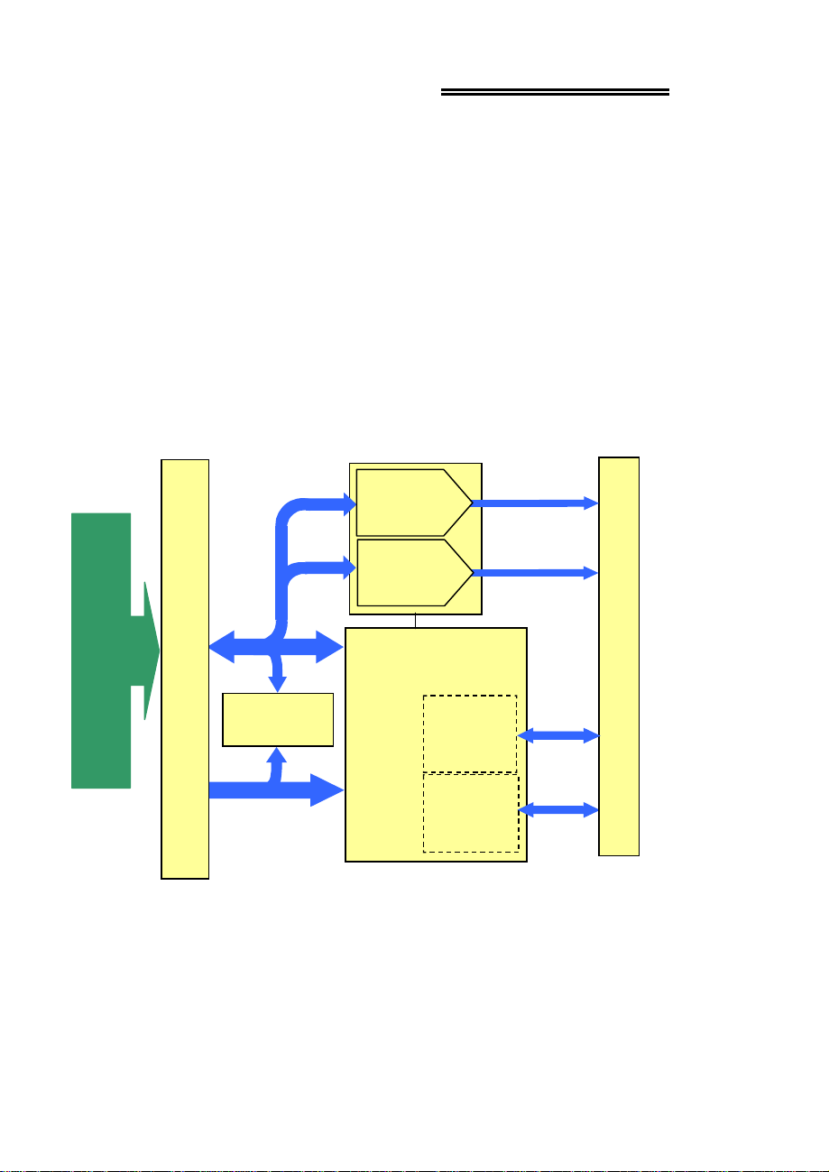
1 INTRODUCTION
(
)
P2 CONNECTOR (15 PIN)
The PCM-DAC02 is an analog output control board for IBM PC compatible
computers with PCMCIA type slots. The heart of the board is a dual 12-bit digital-toanalog converter. Analog voltage signals are generated by the D/A from registers.
Control of I/O operations is done by the Field Programmable Gate Array (FPGA) on
the board (Figur e 1-1). Double-bufferi ng of the output registers permit simultaneous
output changes.
Ranges of the two analog outputs are individually programmable for bipolar ±5V or
±10V, or unipolar 0 to 5V or 0 to 10V.
Eight bi-directional digital I/O lines arranged in two, 4-bit p orts p ro vide the capab ility
of sensing and controlling discrete events. The ports can be programmed to be eight
inputs, eight outputs, or four inputs and four outputs.
HOST BUS ADAPTER
PCMCIA BUS CONNECTOR P1
68-PIN
DATA
BUS
ATTRIBUTE
MEMORY
ADDRESS
BUS
D/A
CONVERTER
12-BIT
D/A
CONVERTER
12-BIT
CONTROLLER
FPGA
PCM-DAC02
Figure 1-1. PCM-DAC02 Block Diagram
DIGITAL
I/O
PORT
4 BITS
DIGITAL
I/O
PORT
4 BITS
1
Page 6
2 INSTALLATION
2.1 INSTALL InstaCal™ SOFTWARE
InstaCal is the installation, calibration and test software supplied with the board.
Refer to the Extended Software Installation Manual to install InstaCal.
2.2 INSTALL THE PCMCIA CARD
Your PCM card is completely plug and play. There are no switches or jumpers to set
prior to installation in your computer. Simply follow the steps shown below to install
your PCM hardware.
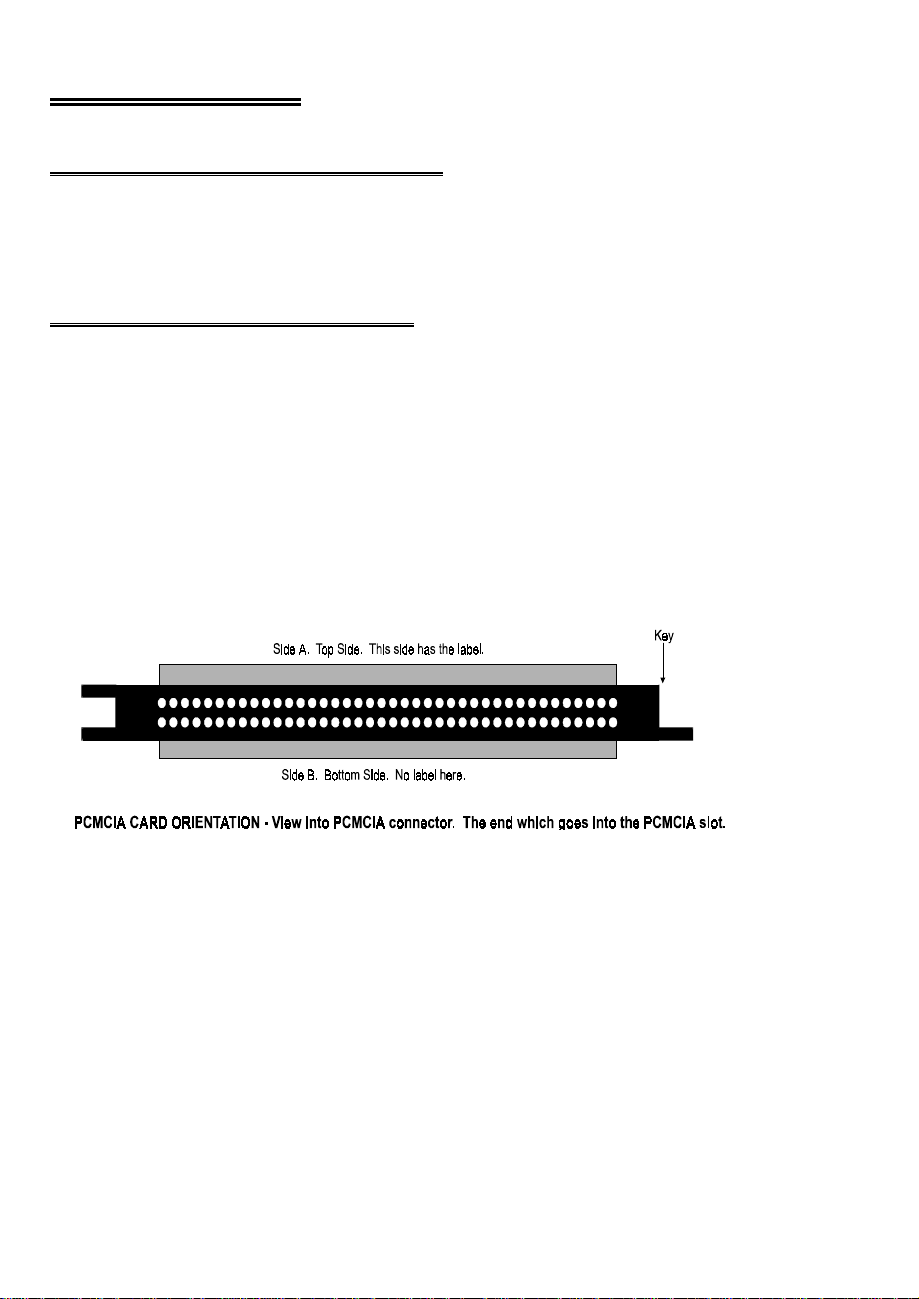
1. Insert the card into a free PC Card/PCMCIA type II or III slot. You do not
have to turn the computer off. The system is designed for power on
installation. Shown here is a PCM card case looking into the connector
which is inserted into the PCMCIA slot of your computer. The KEY helps to
insure that the PCM board is inserted in the correct orientation.
2. If the appropriate driver is already loaded on the PC, the card should be
detected, recognized, and configured by Windows and you should hear an
insertion beep. To verify the card has been recognized, go to Control
Panel\System\Device Manager and the card should now appear under "DAS
Component."
2
Page 7

3 INTERFACING
The PCM-DAC02 connector has two single-ended analog outputs, one interrupt input,
eight digital inputs/outputs and three ground pins. A chassis ground is in the cable
shield clips to either side of the 15 pins of the connector.
3.1 PCM-DAC02 CONNECTOR
Figure 3-1 shows a PCM-DAC02 case looking into the connector. The KEY helps to
insure that the cable is inserted in the correct orientation.
Figure 3-1. PCM-DAC02 I/O Connector
Analog devices to be controlled should be connected with the high side to the
numbered analog output and the low side to an adjacent ground.
3
Page 8

3.2 CONNECTING DEVICES TO THE ANALOG OUTPUTS
The PCM-DAC02 analog outputs are single ended. When connecting analog output
channels, use pin 1 gr ound for channe l 0 (pin 2) , and pin 3 ground for cha nnel 1 (pin
4).
You must avoid potentials between signal ground and chassis ground on your
computer. If you are using a laptop and are on battery power, the computer is floating
with respect to earth ground, but the laptop is on the charger unit or on wall power, the
laptop may be grounded.
Whenever the computer is grounded, you must connect signals so there is no potential
between PC ground and signal ground. If there is a potential, it will be added to the
signal. For example, if your PCM-DAC02 is supplying 3.5 volts and there is a
potential of -1.5V between the PC and the sensor ground, your device under control
will be reading 2.0V instead of 3.5V
3.3 OUTPUT VOLTAGE RANGES
There are four possible output voltage ranges. Each DAC can be controlled
independently, meaning that each DAC may have a different range. The output
voltage range is controlled by software. To learn about c ontrolling the output r ange of
the DACs please consult your software manual, either Universal library for
programmers, or your Labtech or other package application user's manual.
The available ranges are:
Range
0 to 5V 0.00122 V 0 V 2.50V 4.99878V
0 to 10V 0.00244 V 0 V 5.00V 9.9976V
±5V 0.00244 V
±10V 0.00488 V
LSB Step Size 0 Code 2048 Code 4095 Code
−
5 V 0 V 4.9976V
−
10V 0 V 9.9951V
3.4 SIGNAL CONNECTION
The outputs of the PCM-DAC02 are two-wire voltages. There is a polarity associated
with the two wires and thus the outputs are labeled Analog Out Channel # and
Ground, on the c onnector. In unipola r mode, the o utput high and the gr ound line ar e
at the same level when the DAC code is zero. In bipolar mode, the output high and
ground are the same at a code of 2048.
4
Page 9

The maximum current supplied by the analog outputs is 2.5 mA. Loads drawing
higher currents than this will cause the analog output to droop, meaning that a code of
4095 will not be able to generate a full scale voltage of 5V, but one somewhat less.
It is best to group the ground on pin 1 with the analog output on pin 2, and the ground
on pin 3 with the analog output on pin 4
3.5 EXTERNAL INTERRUPT INPUT
The PCM-DAC02 pin 5 is the input to a circuit which will generate an interrupt to the
computer. The interrupt must be enabled through software. The interrupt is level
sensitive and is triggered on a TTL high level. T TL high is approximately 2.5V to
5V. The interrupt signal you provide sho uld transition from a low of 0, or ground, to
a high of 5V.
The procedure initiated by an interrupt is wholly dependent on programming.
3.6 DIGITAL INPUTS & OUTPUTS
The PCM-DAC02 has eight bi-directional digital I/O lines. The eight digital lines
may be programmed as input or output in groups of: eight inputs, eight outputs or four
inputs and four outputs.
A register controls the direction of the digital I/O lines and must be set via software.
At power on or reset the digital lines default to inputs.
Please note: Digital lines in an input state present a high impedance to any device
connected to them. The implication is that if you are using a digital line to control the
input of a TTL chip, and that digital line turns from an output to an input, the T TL
chip being controlled MAY detect the turned around line as a “1” or a “0”. This could
cause the TTL input being controlled to switch on or off, possibly with consequences
for the system you are controlling. To prevent random switching and force all digital
lines into a known state on power up or reset, use pull up or pull down resistors to fix
the state of the line as either high or low. A properly selected resistor will not interfere
with TTL level output signals.
For more information on programming the digital I/O lines, please refer to the
Universal library programmers manual.
5
Page 10

4 PROGRAMMING & APPLICATIONS
4.1 PROGRAMMING LANGUAGES
Universal Library provides complete access to the PCM-DAC02 functions from a
range of programming languages; both DOS and Windows. If you are planning to
write programs, or would like to run the example programs for Visual Basic or any
other language, please turn now to the Universal library manual.
4.2 PACKAGED APPLICATIONS PROGRAMS
Many packaged application programs, such as SoftWIRETM, have drivers for the
PCM-DAC02. If the package you own does not appear to have drivers you need,
please fax the package name and the revision number from the install disks. We will
research the package for you and advise by return fax how to obtain necessary drivers.
6
Page 11

5 CALIBRATION
The PCM-DAC02 is hardware calibrated and tested at the factory. All calibration
after initial manufacturing is done via software. The calibration factors are stored on
the PCM-DAC02 and should be applie d thro ugh software ever y time the board is r un.
Never attempt to open the case since there are no parts inside that you can service.
There are no socketed components.
If you are using the Universal library, you can set software calibration factors for
offset and gain using the Calibration option of InstaCal. These factors will be applied
to outputs made by any of the D/A routines called from any of the language libr aries
of Universal library.
You will need a precision calibrated DVM having better than 1/4096 resolution.
After calibration factors are set, they are stored in the PCM-DAC02. These
calibration factors are accessed by Universal library and InstaCal and applied to any
output codes sent to the PCM-DAC02. If you use direct register programming be sure
to access and apply the calibration factors.
Calibration factors may be reset at any time by running InstaCal calibration. Choose
Calibration from the InstaCal menu, and follow the instructions. Press F1 for help.
7
Page 12

6 I/O ADDRESS MAP & REGISTER FUNCTIONS
A base address register controls the beginning, or 'Base Address' of the I/O addresses
occupied by the control registers of the PCM-DAC02. Seven addresses are occupied.
The base address assigned by CSS is stored in the CB.CBG file by InstaCal.
CONTROL REGISTERS
After CSS is installed and a base address has been established, the PCM-DAC02 can
be controlled by writing to and reading from the control registers. W hile it is p ossib le
to write your own control routines for the PCM-DAC02, routines have been written
and are available in Universal libr ary for D OS and Wind ows progr amming languages.
NOTE ON REGISTER PROGRAMMING SUPPORT
While the complete register map is explained here, only very limited support for
assembly language or direct register programming is available. Register level
programming should only be done by experienced programmers. We support the use
of the PCM-DAC02 through high level languages using Universal Library.
BASE + 0 - DAC0 LSB Data Register
Any write to this register will trigger an A/D conversion. This is a good method of
starting conversions from software or time-of-day clock control.
WRITE: D/A Data can be written to this address and to Base + 1 to form a 12-bit
D/A data word.
01234567
D/A0D/A1D/A2D/A3D/A4D/A5D/A6D/A7
READ: Clears interrupt.
BASE + 1 - DAC0 MSB (4 bits)
WRITE: Send DAC data. & Update outputs of DAC0
01234567
D/A8D/A9D/A10D/A11XXXX
READ: Calibration: read status (Busy: 0 = busy, 1 = ready)
01234567
BUSYXXXXXXX
BASE + 2 - DAC1 LSB Data Register
8
Page 13

WRITE: Same as base + 0 but for second DAC, DAC1.
READ: No function
01234567
D/A0D/A1D/A2D/A3D/A4D/A5D/A6D/A7
BASE + 3 - DAC1 MSB (4 bits)
WRITE: Same as base + 1 but for second DAC, DAC1. Updates DAC1.
READ: No function
01234567
D/A8D/A9D/A10D/A11XXXX
BASE + 4 - Digital I/O (8 bits)
WRITE: Updates output of DIO bits set for output.
READ: Reads current status of DIO bits set for input. Reads back output state of
DIO bits set for output.
01234567
DIO0DIO1DIO2DIO3DIO4DIO5DIO6DIO7
BASE + 5 - Calibration Data Load Register
WRITE: Load bit for calibration DAC, which is serial load.
READ: Writes contents of DATA into the DAC8800.
01234567
DATAXXXXXXX
For a complete technical description of the calibration procedure please fax your
request to Measurement Computing Corp., attention of the Engineering Manager. The
details of this procedure are available to any software developer desiring to add a
calibration routine for the PCM-DAC02.
BASE + 6 - Control & Status Register
WRITE: Loads various control bits, explained below.
READ: Reads status of various control bits, explained below.
Set DAC Output Range DAC#R1 DAC#R0
±5V 0 0
±10V 0 1
9
01234567
DAC1R0DAC1R1DAC0R0DAC0R1LDIRUDIRINT_ENX
01234567
DAC1R0DAC1R1DAC0R0DAC0R1LDIOUDIOINT_ENEXT_INT
Page 14

0 to 5V 1 0
0 to 10V 1 1
UDIO & LDIO
Set the direction of the upper and lower four bits of the digital I/O lines. Set to “1”
for output; set to “0” for input. Digital I/O defaults to input on power up
INT_EN
Enable interrupt from pin 5. Enable = “1”. Disable = “0”
EXT_INT
Set to “1” when an interrupt has been detected on pin 5. Interrupt is level only.
Interrupt occurs at TTL high (2.5V < TTL High < 5V). Reading base+0 clears this bit.
10
Page 15

7 SPECIFICATIONS
Typical for 25°C unless otherwise specified.
POWER CONSUMPTION
+5V (Normal operation) 48 mA typ, 65 mA max
+5V (During CIS read) 65 mA typ, 105 mA max
ANALOG OUTPUT
D/A converter type AD7837 Dual MDAC
Resolution 12 bits
Number of channels 2
Output Ranges ±10V, ±5V, 0 to 10V, 0 to 5V, each
channel individually programmable
D/A pacing Software paced
D/A trigger modes Software
Data transfer Programmed I/O
Offset error (calibrated) ±1 LSB
Gain error (calibrated) ±1 LSB
Differential non-linearity (D/A spec) ±1 LSB
Integral non-linearity (D/A spec) ±1 LSB
Monotonicity Guaranteed monotonic
Throughput System-dependent
Slew rate 7.2 V/µsec typ
Settling time (to ½ LSB of FSR) 8 µs typ
Current Drive ±2.5 mA
Output short-circuit duration 15 mA indefinite
Output coupling DC
Miscellaneous Double-buffered output latches
DIGITAL I/O
Digital type FPGA
11
Page 16

Configuration Two ports, four bits each.
Programmable as 8 input, 8 output
or 4 input and 4 output
Input low voltage 0.8V max
Input high voltage 2.0V min
Output low voltage (IOL = 4 mA) 0.23V max
Output high voltage (IOH = −4 mA) 3.86V min
Absolute maximum input voltage −0.5V , +5.5V
Interrupt Enable Programmable
Interrupt Source External (Ext Int), falling edge triggered,
cleared by a read of Base + 0 address
ENVIRONMENTAL
Operating temperature range 0 to 70°C
Storage temperature range −40 to 100°C
Humidity 0 to 90% non-condensing
12
Page 17

8 PCM-C15-10-INCH CABLE
The PCM-C15-10-INCH is a 10-inch 15-pin cable assembly for use with a 15-pin
PCMCIA cards. The PCM-C15-10-INCH has a connector on one end and open
terminations at the other end for user field wiring. The chart below lists color coding.
COLORPINCOLORPIN
Purple9Black1
Gray10White2
Lt. Brown11Red3
Pink12Green4
White/Blue13Brown5
Blue/White14Blue6
Green/Yellow15Orange7
BareSHIELDYellow8
13
Page 18

For your notes
Page 19

EC Declaration of Conformity
We, Measurement Computing Corporation, declare under sole responsibility that the
product:
PCMCIA Dual-Channel Analog Output
BoardPCM-DAC02
DescriptionPart Number
to which this declaration relates, meets the essential requirements, is in conformity
with, and CE marking has been applied according to the relevant EC Directives listed
below using the relevant section of the following EC standards and other normative
documents:
EU EMC Directive 89/336/EEC
compatibility.
EU 55022 Class B
characteristics of information technology equipment.
EN 50082-1
IEC 801-2
and control equipment.
IEC 801-3
measurements and control equipment.
IEC 801-4
equipment.
Carl Haapaoja, Director of Quality Assurance
: Electrostatic discharge requirements for industrial process measurement
: Radiated electromagnetic field requirements for industrial process
: Electrically fast transients for industrial process measurement and control
: Limits and methods of measurements of radio interference
: EC generic immunity requirements.
: Essential requirements relating to electromagnetic
Page 20

Measurement Computing Corporation
16 Commerce Boulevard,
Middleboro, Massachusetts 02346
(508) 946-5100
Fax: (508) 946-9500
E-mail: info@measurementcomputing.com
www.measurementcomputing.com
 Loading...