

Page 1

Page 2

PCIM-DAS16JR/16
Analog & Digital I/O Board
User's Guide
Document Revision 3, May, 2006
© Copyright 2006, Measurement Computing Corporation
Page 3

Your new Measurement Computing product comes with a fantastic extra —
Management committed to your satisfaction!
Refer to www.mccdaq.com/execteam.html for the names, titles, and contact information of each key executive at Measurement
Computing.
Thank you for choosing a Measurement Computing product—and congratulations! You own the finest, and you can now enjoy
the protection of the most comprehensive warranties and unmatched phone tech support. It’s the embodiment of our two
missions:
! To offer the highest-quality, computer-based data acquisition, control, and GPIB hardware and software available—at
the best possible price.
! To offer our customers superior post-sale support—FREE. Whether providing unrivaled telephone technical and sales
support on our latest product offerings, or continuing that same first-rate support on older products and operating
systems, we’re committed to you!
Lifetime warranty: Every hardware product manufactured by Measurement Computing Corporation is warranted against
defects in materials or workmanship for the life of the product. Products found defective are repaired or replaced promptly.
Lifetime Harsh Environment Warranty®: We will replace any product manufactured by Measurement Computing
Corporation that is damaged (even due to misuse) for only 50% of the current list price. I/O boards face some tough operating
conditionssome more severe than the boards are designed to withstand. When a board becomes damaged, just return the unit
with an order for its replacement at only 50% of the current list price. We don’t need to profit from your misfortune. By the way,
we honor this warranty for any manufacturer’s board that we have a replacement for.
30 Day Money Back Guarantee: You may return any Measurement Computing Corporation product within 30 days of
purchase for a full refund of the price paid for the product being returned. If you are not satisfied, or chose the wrong product by
mistake, you do not have to keep it. Please call for an RMA number first. No credits or returns accepted without a copy of the
original invoice. Some software products are subject to a repackaging fee.
These warranties are in lieu of all other warranties, expressed or implied, including any implied warranty of merchantability or
fitness for a particular application. The remedies provided herein are the buyer’s sole and exclusive remedies. Neither
Measurement Computing Corporation, nor its employees shall be liable for any direct or indirect, special, incidental or
consequential damage arising from the use of its products, even if Measurement Computing Corporation has been notified in
advance of the possibility of such damages.
HM PCIM-DAS16jr_16.doc
ii
Page 4

Trademark and Copyright Information
TracerDAQ, Universal Library, InstaCal, Harsh Environment Warranty, Measurement Computing Corporation, and the
Measurement Computing logo are either trademarks or registered trademarks of Measurement Computing Corporation.
Windows, Microsoft, and Visual Studio are either trademarks or registered trademarks of Microsoft Corporation
LabVIEW is a trademark of National Instruments.
CompactFlash is a registered trademark of SanDisk Corporation.
All other trademarks are the property of their respective owners.
Information furnished by Measurement Computing Corporation is believed to be accurate and reliable. However, no
responsibility is assumed by Measurement Computing Corporation neither for its use; nor for any infringements of patents or
other rights of third parties, which may result from its use. No license is granted by implication or otherwise under any patent or
copyrights of Measurement Computing Corporation.
All rights reserved. No part of this publication may be reproduced, stored in a retrieval system, or transmitted, in any form by any
means, electronic, mechanical, by photocopying, recording, or otherwise without the prior written permission of Measurement
Computing Corporation.
Notice
Measurement Computing Corporation does not authorize any Measurement Computing Corporation product for use
in life support systems and/or devices without prior written consent from Measurement Computing Corporation.
Life support devices/systems are devices or systems which, a) are intended for surgical implantation into the body,
or b) support or sustain life and whose failure to perform can be reasonably expected to result in injury.
Measurement Computing Corporation products are not designed with the components required, and are not subject
to the testing required to ensure a level of reliability suitable for the treatment and diagnosis of people.
iii
Page 5

Table of Contents
Preface
About this User's Guide ......................................................................................................................vi
What you will learn from this user's guide ........................................................................................................vi
Conventions in this user's guide....................................................................................................................................... vi
Where to find more information........................................................................................................................vi
Chapter 1
Introducing the PCIM-DAS16JR/16 .................................................................................................1-1
Overview: PCIM-DAS16JR/16 features ........................................................................................................ 1-1
Software features............................................................................................................................................ 1-1
Chapter 2
Installing the PCIM-DAS16JR/16 ..................................................................................................... 2-1
What comes with your PCIM-DAS16JR/16 shipment? ................................................................................. 2-1
Hardware ....................................................................................................................................................................... 2-1
Additional documentation.............................................................................................................................................. 2-1
Optional components ..................................................................................................................................................... 2-2
Unpacking the PCIM-DAS16JR/16................................................................................................................ 2-2
Installing the software .................................................................................................................................... 2-2
Default hardware configuration...................................................................................................................... 2-2
Channel mode switch..................................................................................................................................................... 2-3
A/D trigger edge jumper................................................................................................................................................ 2-4
Clock frequency jumper................................................................................................................................................. 2-4
Installing the PCIM-DAS16JR/16.................................................................................................................. 2-5
Connecting the board for I/O operations ........................................................................................................ 2-5
Connectors, cables – main I/O connector....................................................................................................................... 2-5
Pin out – main I/O connector ......................................................................................................................................... 2-6
Cabling........................................................................................................................................................................... 2-6
Field wiring, signal termination, and signal conditioning.............................................................................................. 2-7
Chapter 3
Programming and Developing Applications .................................................................................. 3-1
Programming languages ................................................................................................................................. 3-1
Packaged applications programs..................................................................................................................... 3-1
Register-level programming ........................................................................................................................... 3-1
Chapter 4
Functional Details ............................................................................................................................. 4-1
Analog inputs.................................................................................................................................................. 4-2
Burst mode..................................................................................................................................................................... 4-2
Digital I/O....................................................................................................................................................... 4-3
Counter/timer I/O ........................................................................................................................................... 4-3
Chapter 5
Calibrating the PCIM-DAS16JR/16 .................................................................................................. 5-1
Calibrating the A/D & D/A converters........................................................................................................... 5-1
Required equipment.......................................................................................................................................................5-1
Chapter 6
Specifications.................................................................................................................................... 6-1
Power consumption ........................................................................................................................................ 6-1
Analog input ................................................................................................................................................... 6-1
iv
Page 6

PCIM-DAS16JR/16 User's Guide
Accuracy........................................................................................................................................................................ 6-2
Analog input drift........................................................................................................................................................... 6-2
Noise performance......................................................................................................................................................... 6-2
Settling time................................................................................................................................................................... 6-3
Digital input / output....................................................................................................................................... 6-3
Main connector .............................................................................................................................................................. 6-3
Counter ........................................................................................................................................................... 6-4
Environmental ................................................................................................................................................ 6-4
Mechanical ..................................................................................................................................................... 6-4
Main connector and pin out............................................................................................................................ 6-4
8-channel differential mode pin out ............................................................................................................................... 6-5
16-channel single-ended mode pin out........................................................................................................................... 6-5
v
Page 7

About this User's Guide
What you will learn from this user's guide
This user's guide explains how to install, configure, and use the PCIM-DAS16JR/16 so that you get the most
out of its analog, digital, and counter I/O features.
This user's guide also refers you to related documents available on our web site, and to technical support
resources.
Conventions in this user's guide
For more information on …
Text presented in a box signifies additional information and helpful hints related to the subject matter you are
reading.
Caution! Shaded caution statements present information to help you avoid injuring yourself and others,
damaging your hardware, or losing your data.
Preface
<#:#> Angle brackets that enclose numbers separated by a colon signify a range of numbers, such as those assigned
to registers, bit settings, etc.
bold text Bold text is used for the names of objects on the screen, such as buttons, text boxes, and check boxes. For
example:
1. Insert the disk or CD and click the OK button.
italic text Italic text is used for the names of manuals and help topic titles, and to emphasize a word or phrase. For
example:
The InstaCal installation procedure is explained in the Quick Start Guide.
Never touch the exposed pins or circuit connections on the board.
Where to find more informati on
Additional information about USB-201 hardware is available on our website at www.mccdaq.com. You can
also contact Measurement Computi ng Corporation with specific questions.
Knowledgebase: kb.mccdaq.com
Phone: 508-946-5100 and follow the instructions for reaching Tech Support
Fax: 508-946-9500 to the attention of Tech Support
Email:
techsupport@mccdaq.com
vi
Page 8

Chapter 1
Introducing the PCIM-DAS16JR/16
Overview: PCIM-DAS16JR/16 features
This manual explains how to install and use the PCIM-DAS16JR/16 board. The PCIM-DAS16JR/16 is a
multifunction measurement and control board designed to operate in computers with PCI accessory slots. This
board can be used for applications such as data acquisition, system timing, and industrial process control.
The PCIM-DAS16JR/16 provides the following features:
! Eight differential or 16 single-ended analog inputs
! 16-bit A/D resolution
! 100 kHz sample rate
! Eight TTL-compatible digital I/O channels
! Three 16-bit down counters
! 37-pin high density I/O connector
! Universal PCI bus (3.3V/5V 32-bit 33 MHz)
The analog input mode is switch-selectable for eight differential or 16 single-ended analog inputs. Analog input
ranges are selectable with software as bipolar or unipolar. Bipolar input ranges are ±10V, ±5V, ±2.5V and
±1.25V. Unipolar input ranges are 0 to 10V, 0 to 5V, 0 to 2.5V and 0 to 1.25V.
The PCIM-DAS16JR/16 board is equipped with an 82C54 counter chip. This chip contains three 16-bit down
counters that provide clock, gate, and output connections.
Software features
For information on the features of InstaCal and the other software included with your PCIM-DAS16JR/16, refer
to the Quick Start Guide that shipped with your device. The Quick Start Guide is also available in PDF at
www.mccdaq.com/PDFmanuals/DAQ-Software-Quick-Start.pdf
Check www.mccdaq.com/download.htm
under less commonly used operating systems.
for the latest software version or versions of the software supported
.
1-1
Page 9

Installing the PCIM-DAS16JR/16
What comes with your PCIM-DAS16JR/16 shipment?
The following items are shipped with the PCIM-DAS16JR/16.
Hardware
! PCIM-DAS16JR/16
Chapter 2
Additional documentation
In addition to this hardware user's guide, you should also receive the Quick Start Guide (available in PDF at
www.mccdaq.com/PDFmanuals/DAQ-Software-Quick-Start.pdf
the software you received with your PCIM-DAS16JR/16 and information regarding installation of that software.
Please read this booklet completely before installing any software or hardware.
2-1
). This booklet supplies a brief description of
Page 10

PCIM-DAS16JR/16 User's Guide Installing the PCIM-DAS16JR/16
Optional components
If you ordered any of the following products with your board, they should be included with your shipment.
! Cables
C37FF-x
! Signal termination and conditioning accessories
MCC provides signal termination products for use with the PCIM-DAS16JR/16. Refer to the "Field wiring,
signal termination and signal conditioning" section on page 2-7 for a complete list of compatible accessory
products.
C37FFS-x
Unpacking the PCIM-DAS16JR/16
As with any electronic device, you should take care while handling to avoid damage from static
electricity. Before removing the PCIM-DAS1602/16 from its packaging, ground yourself using a wrist strap or
by simply touching the computer chassis or other grounded object to eliminate any stored static charge.
If any components are missing or damaged, notify Measurement Computing Corporation immediately by
phone, fax, or e-mail:
! Phone: 508-946-5100 and follow the instructions for reaching Tech Support.
! Fax: 508-946-9500 to the attention of Tech Support
! Email: techsupport@mccdaq.com
Installing the software
Refer to the Quick Start Guide for instructions on installing the software on the Measurement Computing Data
Acquisition Software CD. This booklet is available in PDF at www.mccdaq.com/PDFmanuals/DAQ-Software-
Quick-Start.pdf.
Configuring the PCIM-DAS16JR/16
The PCIM-DAS16JR/16 board has one switch and two jumpers mounted on it. Before installing the PCIMDAS16JR/16 in the computer, verify that the board is configured with the settings that you want. Factory
default settings are listed in T . able 2-1
Table 2-1. Switch/jumper factory-configured defaults
Board label Switch/jumper description Default setting
S1 Channel mode switch 8 channel (diff)
P8 A/D Trigger edge jumper Rising edge
P2 Clock frequency jumper 1 MHz
The locations of each switch and jumper are shown in . Figure 2-1
2-2
Page 11

PCIM-DAS16JR/16 User's Guide Installing the PCIM-DAS16JR/16
A
/D trigger edge
jumper
Channel mode
switch
Clock frequency
jumper
Figure 2-1. PCIM-DAS16JR/16 switch and jumper locations
Instructions on how to change the configuration of each jumper and switch are shown on the following pages.
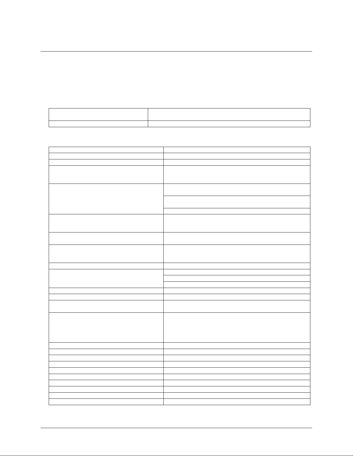
Channel mode switch
Switch S1 configures the analog inputs of the PCIM-DAS16JR/16 as either eight differential channels or
16 single-ended channels. Set the switch to single-ended mode if you have more than eight analog inputs to
sample. Setting the switch to differential mode allows up to 10 volts of common mode (ground loop) rejection
and provides better noise immunity.
The channel mode switch is factory-configured for eight differential inputs (see Fi .) To configure for
16 single-ended channels, set this switch to "
SE".
DIFF
S1
Figure 2-2. Channel mode switch
SE
gure 2-2
2-3
Page 12
PCIM-DAS16JR/16 User's Guide Installing the PCIM-DAS16JR/16
A/D trigger edge jumper
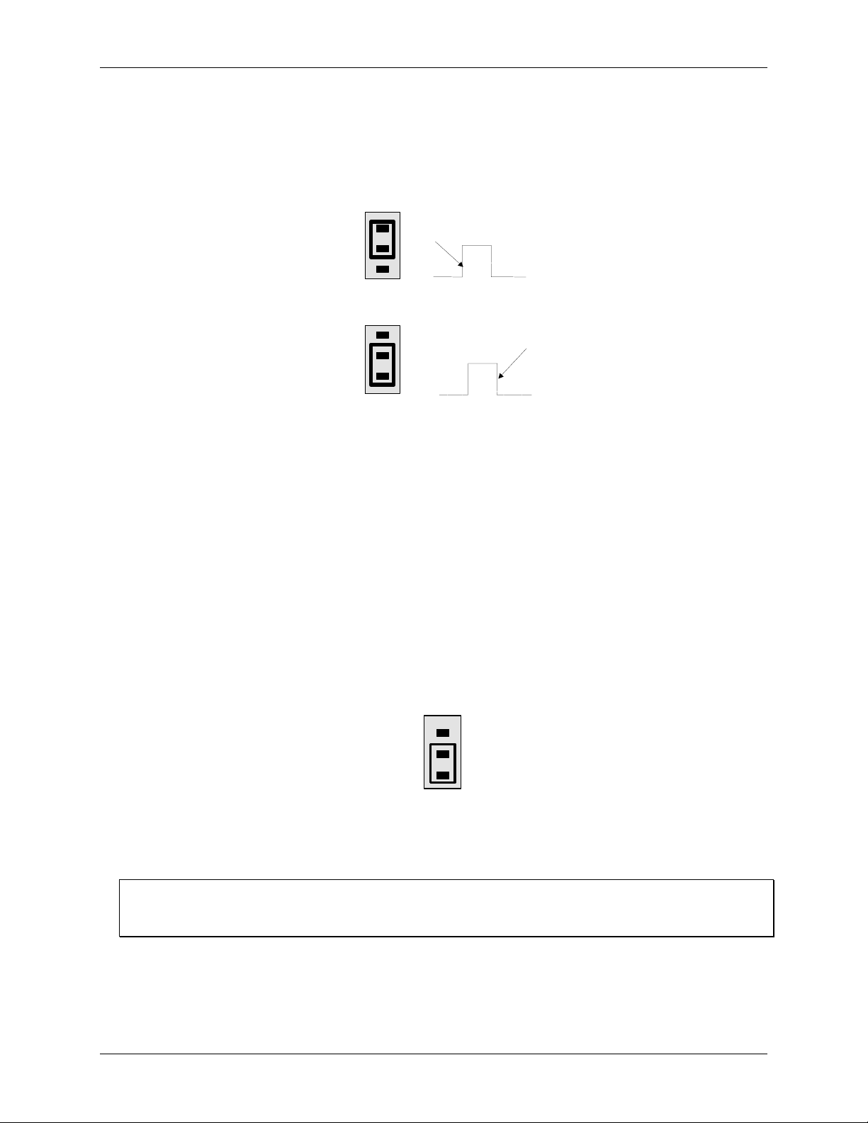
Jumper P8 configures the edge to initiate the A/D conversion with. The options are either rising or falling edge.
The A/D trigger edge jumper is factory-configured for rising edge. shows the jumper position for
each configuration option.
Rising edge A/D trigger
R
F
P8
DAS-16 method
Figure 2-3
Default
setting
R
F
P8
P8
Figure 2-3. A/D trigger edge jumper
Falling edge A/D trigger
DAS-16 method
For compatibility with all third-party packages, DAS-16 software, and PCIM-DAS16JR/16 software, leave this
jumper set to the default rising edge position.
If you are using the PCIM-DAS16JR/16 board in an application that is designed for compatibility with the
Keithley MetraByte DAS-1600 board, configure the trigger edge jumper for falling edge.
Clock frequency jumper
Jumper P2 configures the frequency of the square wave that is used as a clock by the A/D pacer circuitry. This
pacer circuitry controls the sample timing of the A/D.
You can configure the frequency for 10 MHz or 1 MHz. The clock frequency jumper is factory-configured for 1
MHz, as shown in . Figure 2-4
10M CLK SEL
P2
1M
Figure 2-4. Clock frequency jumper
Configure this jumper for 10 MHz, unless you have reason to do otherwise.
The internal pacer output is also available at pin 20
The internal pacer output that drives the A/D converter is also available at pin 20 (CTR 3 Output) on the board's
main I/O connector (see Figure 2-5).
2-4
Page 13

PCIM-DAS16JR/16 User's Guide Installing the PCIM-DAS16JR/16
Installing the PCIM-DAS16JR/16
After you configure the board's switches and jumpers, install the PCIM-DAS16JR/16 into your computer. To
install your board, follow the steps below:
Install the MCC DAQ software before you install your board
The driver needed to run your board is installed with the MCC DAQ software. Therefore, you need to install the
MCC DAQ software before you install your board. Refer to the Quick Start Guide for instructions on installing
the software.
Turn your computer off, open it up, and insert your board into any available PCI slot.
1.
Close your computer and turn it on.
2.
If you are using an operating system with support for plug-and-play (such as Windows 2000 or Windows
XP), a dialog box pops up as the system loads indicating that new hardware has been detected. If the
information file for this board is not already loaded onto your PC, you will be prompted for the disk
containing this file. The MCC DAQ software contains this file. If required, insert the Measurement
Computing Data Acquisition Software CD and click
3.
To test your installation and configure your board, run the InstaCal utility installed in the previous section.
Refer to the DAQ Software Quick Start that came with your board for information on how to initially set up
and load InstaCal.
OK.
Board configuration with InstaCal
If you change the board configuration with InstaCal, you may have to also physically change the setting of a
corresponding switch or jumper on the board. Refer to Default hardware configuration on page 2-2 for specific
jumper and switch information.
Allow your computer to warm up for at least 15 minutes before acquiring data. The high speed components
used on the board generate heat, and it takes this amount of time for a board to reach steady state if it has been
powered off for a significant amount of time.
Connecting the board for I/O operations
Connectors, cables – main I/O connector
Table 2-2
DAS16JR/16.
Connector type 37 pin male "D" connector
Connector compatibility Identical to the CIO-DAS16JR/16 connector
Compatible cables C37FF-x (Figure 2-6)
Compatible accessory products
(with the C37FF-x cable or C37FFs-x cable)
lists the board connectors, applicable cables, and compatible accessory products for the PCIM-
Table 2-2. Board connectors, cables, accessory equipment
C37FFS-x (Figure 2-7)
CIO-MINI37
SCB-37
CIO-SSH16
The PCIM-DAS16JR/16 board's main I/O connector is a 37-pin "D" connector that is accessible from the rear
of the PC on the expansion back plate. This connector accepts female 37-pin D-type connectors, such as the
C37FF-x 37-pin cable (Figure 2-6) or the C37FFS-x 37-pin shielded cable (Figure 2-7).
Analog connections and configuration
General information on analog signal connections and configuration is contained in the Guide to Signal
Connections (available on our web site at www.mccdaq.com/signals/signals.pdf).
2-5
Page 14

PCIM-DAS16JR/16 User's Guide Installing the PCIM-DAS16JR/16
Pin out – main I/O connector
CTR 1 Clock In
DIG Out 2
DIG Out 0
DIG In 2/CTR1 Gate
SS&H Out
N/C
AGND
AGND
CH7 High
CH6 High
CH5 High
CH4 High
CH3 High
CH2 High
CH1 High
CH0 High
PCI Slot
20
21
22
23
24
25
26
27
28
29
30
31
32
33
34
35
36
37
+5V PC Bus Power
CTR 1 OUT
DIG Out 3
DIG Out 1
DIG In 3
DIG In 1
DIG Gnd
N/C
N/C
N/C
Low
Ch7 / Ch15 High
Low High
Ch6 / Ch14
Low High
Ch5 / Ch13
Low High
Ch4 / Ch12
Low High
Ch3 / Ch11
Low High
Ch2 / Ch10
Low High
Ch1 / Ch9
Ch0 Low / Ch8
A
GND
High
Figure 2-5. Main I/O connector
Cabling
You can use the C37FF-x or C37FFS-x 37-pin cable to connect signals to the PCIM-DAS16JR/16 board.
The red stripe
1
20
37
19
identifies pin # 1
1
19
20
37
Figure 2-6. C37FF-x cable
1
20
19
37
1
20
19
37
Figure 2-7. C37FFS-x cable
2-6
Page 15

PCIM-DAS16JR/16 User's Guide Installing the PCIM-DAS16JR/16
Field wiring, signal termination, and signal conditioning
You can use the following MCC screw terminal boards to terminate field signals and route them into the PCIMDAS16JR/16 board using a C37FF-x cable or a C37FFS-x cable:
! CIO-MI
! SCB-37
pin connections.
NI37 – 4 x 4, 37-pin screw terminal board.
– 37-conductor, shielded signal connection/screw terminal box that provides two independent 37-
.
.
2-7
Page 16

Chapter 3
Programming and Developing Applications
After following the installation instructions in Chapter 2, your board should now be installed and ready for use.
Although the board is part of the larger DAS family, in general there may be no correspondence among
registers for different boards. Software written at the register level for other DAS models will not function
correctly with your board.
Programming languages
Measurement Computing’s Universal Library™ provides access to board functions from a variety of Windows
programming languages. If you are planning to write programs, or would like to run the example programs for
Visual Basic
site at www.mccdaq.com/PDFmanuals/sm-ul-user-guide.pdf
Packaged applications programs
Many packaged application programs, such as SoftWIRE and HP-VEE™, now have drivers for your board. If
the package you own does not have drivers for the board, please fax or e-mail the package name and the
revision number from the install disks. We will research the package for you and advise how to obtain drivers.
or any other language, please refer to the Universal Library User's Guide (available on our web
).
Some application drivers are included with the Universal Library package, but not with the application package.
If you have purchased an application package directly from the software vendor, you may need to purchase our
Universal Library and drivers. Please contact us by phone, fax or e-mail:
! Phone: 508-946-5100 and follow the instructions for reaching Tech Support.
! Fax: 508-946-9500 to the attention of Tech Support
! Email: techsupport@mccdaq.com
Register-level programming
You should use the Universal Library or one of the packaged application programs mentioned above to control
your board. Only experienced programmers should try register-level programming. If you need to program at
the register level in your application, refer to the Register Map for the PCIM-DAS16JR/16 (available at
www.mccdaq.com/registermaps/RegMapPCIM-DAS16Jr-16.pdf
).
3-1
Page 17

Functional Details
The PCIM-DAS16JR/16 provides the following features:
! Eight differential or 16 single-ended 16-bit analog inputs
! Eight high current digital I/O channels
! Three 16-bit down counters
The block diagram shown here illustrates the functionality of the PCIM-DAS16JR/16.
Gain and Offset trimpots
Chapter 4
Analog In
16 CH S.E.
8 CH DIFF.
CLK
GATE
OUT
Mux
&
Gain
ADC
Pacer
CTR 2
CTR 1
User
Counter
CTR0
Control
16-Bit,100 kHz
Start EO C
1K
FIFO
INT
FPGA
CONTROLLER
Bus
Timing
LOCAL BUS
Time Base
10MHz
1MHz
BADR1
Boot
EEPROM
PCI BUS (5V/3.3V, Universal 32-BIT, 33MHZ)
PCI
CONTROLLER
BADR2
BADR3
Interrupt
Figure 4-1. PCIM-DAS16JR/16 block diagram
4-1
Page 18

PCIM-DAS16JR/16 User's Guide Functional Details
Analog inputs
The analog input mode is switch-selectable for eight differential or 16 single-ended analog inputs. The board
offers a 100 kHz maximum sample rate in single and multi-channel scans at any gain setting. A 1024 sample
FIFO assures that data taken from the board is transferred into computer memory without the possibility of
missed samples. The board has a digital trigger input with software-selectable trigger edge.
Software selects the bipolar/unipolar input configuration and input range. lists the analog input ranges
Table 4-1
and resolutions for the available input configurations and gains.
Table 4-1. Input range and resolution
Bipolar Range Resolution Unipolar Range Resolution
±10 V 305 µV 0 to 10 V 153 µV
±5 V 153 µV 0 to 5 V 76.3 µV
±2.5 V 76.3 µV 0 to 2.5 V 38.1 µV
±1.25 V 38.1 µV 0 to 1.25 V 19.1 µV
Burst mode
Channel-to-channel skew results from multiplexing the A/D inputs. Channel skew is defined as the time
between consecutive samples. For example, if four channels are sampled at a rate of 1 kHz per channel, the
channel skew is 250 µs (1 ms/4).
Burst mode minimizes channel-to-channel skew by clocking the A/D at the maximum rate between successive
channels. At the 1-ms pulse, channel 0 is sampled. After 10 µs, channel 1 is sampled. Channel 2 is sampled 10
µs after channel 1 is sampled. Channel 3 is sampled 10 µs after channel 2 is sampled. No samples are then taken
until the next 1-ms pulse, when channel 0 is sampled again. In this mode, the rate for all channels is 1 kHz, but
the channel-to-channel skew (delay) is now 10 µs. The minimum burst mode skew/delay on this board is 10 µs
(refer to ). Figure 4-2
Ch0 Ch1 Ch2 Ch3
Ch0 Ch1 Ch2 Ch3
10 Sµ
Delay
The length of the delay between bursts is
Burst mode pacer is
fixed at 10 µS
set by one of the internal counters, or
may be controlled via the external trigger.
Figure 4-2. Burst mode timing
4-2
Page 19

PCIM-DAS16JR/16 User's Guide Functional Details
Digital I/O
Eight TTL-compatible digital I/O channels are available on the main I/O connector. Four of the digital channels
are configured as input. The remaining four are configured as output.
Counter/timer I/O
The PCIM-DAS16JR/16 provides an 82C54 counter chip. This chip contains three 16-bit down counters that
provide clock, gate, and output connections. You can connect the counter clock to the on-board 10 MHz crystal
oscillator, or leave the counter clock unconnected for user input. For more information on the 82C54, visit our
web site at www.mccdaq.com/PDFmanuals/82C54.pdf
.
4-3
Page 20

Chapter 5
Calibrating the PCIM-DAS16JR/16
The PCIM-DAS16JR/16 is shipped fully calibrated from the factory. For normal environments, you should
calibrate your PCIM-DAS16JR/16 board using InstaCal's calibration procedures every six months-to-a year. If
frequent variations in temperature or humidity are common, recalibrate at least every three months. It requires
less than 20 minutes to calibrate the board using InstaCal.
Calibrating the A/D and D/A converters
InstaCal provides step-by-step on-screen instructions to guide you in calibrating your board. You calibrate the
board's A/D converters by applying a known voltage to an analog input channel and adjusting the board’s trim
pots for offset and gain.
Calibrate the PCIM-DAS16JR/16 for the range you intend to use it in. Slight variations in zero and full scale
may result when the range is changed. These variations can be measured and removed in software, if necessary.
Required equipment
To calibrate the PCIM-DAS16JR/16, you need a precision voltage source, or a non-precision source and a 5½
digit digital voltmeter and a few pieces of wire. Use a jeweler’s screwdriver to adjust the trim pots. An extender
card is not required to calibrate the board.
5-1
Page 21
Specifications
Typical for 25 °C unless otherwise specified.
Specifications in italic text are guaranteed by design.
Power consumption
+5V quiescent 500 mA typical, 750 mA max. Does not include the current consumed
through 37-pin I/O connector.
+5V available at 37-pin I/O connector 1 A max, protected with re-settable fuse
Analog input
A/D converter type LTC1605ACSW
Resolution 16 bits
Number of channels 16 single-ended / 8 differential, switch selectable
Input ranges
! Gain is software selectable
! Unipolar / bipolar polarity is software selectable
A/D Pacing (software programmable)
A/D Trigger
(only available when internal pacing selected,
software enable/disable)
A/D Gate (only available when internal pacing
selected, software enable/disable)
Simultaneous Sample and Hold trigger TTL output (pin 26)
Burst mode Software selectable option, burst interval = 10 µS
Data transfer
Interrupt INTA# - mapped to IRQn via PCI BIOS at boot-time
Interrupt enable Programmable through PLX9030
Interrupt polarity Active high level or active low level, programmable through
Interrupt sources
(software programmable)
A/D conversion time 10 µs max.
Throughput 100 kS/s
Input coupling DC
Input bandwidth (all ranges) 325 kHz
Common mode range ±10 V min.
CMRR @ 60 Hz -100 dB typ., -80 dB min
Recommended warm-up time 15 minutes
Input bias current ±3 nA max.
Input impedance 10 M Ohms min.
Absolute maximum input voltage +55/-40V fault protected via input mux.
±10 V, ±5 V, ±2.5 V, ±1.25 V
0 to 10 V, 0 to 5 V, 0 to 2.5 V, 0 to 1.25 V
Internal counter - 82C54.
Positive or negative edge, jumper selectable.
External source (pin 25),
Positive or negative edge, software selectable.
Software polled
External edge trigger (pin 25),
Positive or negative edge, software selectable.
External gate (pin 25),
High or Low level, software selectable.
Logic 0 = Hold, Logic 1 = Sample
Compatible with CIO-SSH16
From 1024 sample FIFO via interrupt w/ REPINSW
Interrupt
Software polled
PLX9030
! End of conversion
! FIFO not Empty
! End of Burst
! End of Acquisition
! FIFO Half Full
Chapter 6
6-1
Page 22

PCIM-DAS16JR/16 User's Guide Specifications
Accuracy
Typical accuracy ±2.3 LSB
Absolute accuracy ±5.0 LSB
Accuracy components
Gain Error Trimmable by potentiometer to 0
Offset Error Trimmable by potentiometer to 0
PGA linearity error ±1.3 LSB typ., ±10.0 LSB max.
Integral Linearity Error ±0.5 LSB typ., ±3.0 LSB max.
Differential Linearity Error ±0.5 LSB typ., ±2.0 LSB max.
Each PCIM-DAS16JR/16 is tested at the factory to ensure the board’s overall accuracy error does not exceed
±5 LSB. Total board error is a combination of gain, offset, differential linearity and integral linearity error. The
theoretical absolute accuracy of the board may be calculated by summing these component errors. Worst case
error is realized only in the unlikely event that each of the component errors are at their maximum level, and
causing error in the same direction.
Analog input drift
Range Analog Input Full-Scale
Gain drift
±10.00 V 2.2 LSB/°C max. 1.8 LSB/°C max. 4.0 LSB/°C max.
±5.000 V 2.2 LSB/°C max. 1.9 LSB/°C max. 4.1 LSB/°C max.
±2.500 V 2.2 LSB/°C max. 2.0 LSB/°C max. 4.2 LSB/°C max.
±1.250 V 2.2 LSB/°C max. 2.3 LSB/°C max. 4.5 LSB/°C max.
0 - 10.00 V 4.1 LSB/°C max. 1.9 LSB/°C max. 6.0 LSB/°C max.
0 - 5.000 V 4.1 LSB/°C max. 2.1 LSB/°C max. 6.2 LSB/°C max.
0 - 2.500 V 4.1 LSB/°C max. 2.4 LSB/°C max. 6.5 LSB/°C max.
0 - 1.250 V 4.1 LSB/°C max. 3.0 LSB/°C max. 7.1 LSB/°C max.
Analog Input Zero drift Overall Analog Input drift
Absolute error change per °C temperature change is a combination of the gain and offset drift of many
components. The theoretical worst case error of the board may be calculated by summing these component
errors. Worst case error is realized only in the unlikely event that each of the component errors are at their
maximum level, and are causing error in the same direction.
Noise performance
The following table summarizes the worst case noise performance for the PCIM-DAS16JR/16. Noise
distribution is determined by gathering 50000 samples with inputs tied to ground at the PCIM-DAS16JR/16
main connector. Data represents both single-ended and differential modes of operation.
Range LSBrms Typical Counts
±10.00 V 1.30 12
±5.000 V 1.30 12
±2.500 V 1.30 12
±1.250 V 1.30 13
0 - 10.00 V 1.80 15
0 - 5.000 V 1.80 15
0 - 2.500 V 1.80 15
0 - 1.250 V 1.80 16
6-2
Page 23

PCIM-DAS16JR/16 User's Guide Specifications
Settling time
Settling time is defined here as the time required for a channel to settle to within a specified accuracy in
response to a full-scale (FS) step. Two channels are scanned at a specified rate with a –FS DC signal presented
to channel 1 and a +FS DC signal presented to channel 0.
Accuracy Condition Range
Same range to
same range
±0.00076%
(±4 LSB)
±10 V Typ. 400 µS 100 µS 10 µS
±5 V Typ. 100 µS 20 µS 10 µS
±2.5 V Typ. 60 µS 12 µS 10 µS
±1.25 V Typ. 50 µS 10 µS
0 to 10 V Typ. 400 µS 100 µS 10 µS
0 to 5 V Typ. 100 µS 20 µS 10 µS
0 to 2 V Typ. 60 µS 12 µS 10 µS
0 to 1.25 V Typ. 50 µS 10 µS
±0.0015%
(±8 LSB)
±0.0061%
(±16 LSB)
Digital input / output
Main connector
Digital output type 5V/TTL compatible
Digital input type 5V/TTL compatible, pulled to logic high via 10 K resistor network
Number of I/O 8
Configuration 4 fixed input, 4 fixed output
Output high voltage 3.8 volts min. @ -32 mA
Output low voltage 0.55 volts max. @ 32 mA
Input high voltage 2.0 volts min., 7 volts absolute max.
Input low voltage 0.8 volts max., -0.5 volts absolute min.
Data transfer Programmed I/O
Power-up / reset state DIG OUT [3:0] - TTL logic low state
6-3
Page 24

PCIM-DAS16JR/16 User's Guide Specifications
Counter
Counter type 82C54
Configuration 3 down counters, 16-bits each
Counter 1 source
(software selectable)
Counter 1 gate External gate from main connector (pin 24*)
Counter 1 output Available at main connector (pin 2)
Counter 2 source
(jumper selectable at P2)
Counter 2 gate
(software enable/disable)
Counter 2 output Internal only, chained to counter 3 source
Counter 3 source Counter 2 output
Counter 3 gate
(software enable/disable)
Counter 3 output Available at main connector (pin 20).
Clock input frequency 10 MHz max.
High pulse width (clock input) 30 ns min.
Low pulse width (clock input) 50 ns min.
Gate width high 50 ns min.
Gate width low 50 ns min.
Input high 2.0 volts min., 5.5 volts absolute max.
Input low 0.8 volts max., -0.5 volts absolute min.
Output high 3.0 volts min. @ -2.5 mA
Output low 0.4 volts max. @ 2.5 mA
Crystal oscillator frequency 10 MHz
Frequency accuracy 50 ppm
! External source from main connector (pin 21*)
! 100 kHz internal source
! Internal 1 MHz
! Internal 10 MHz
External source from main connector (pin 25*)
External source from main connector (pin 25*)
Programmable as ADC Pacer clock.
* Pins 21, 24, and 25 are pulled to logic high via 10 K resistors.
Environmental
Operating temperature ran e g 0 to 70 °C
Storage temperature range -40 to 100 °C
Humidity 0 to 95% non-condensing
Mechanical
Card dimensions PCI half card: 136.5 mm (L) x 106.9 mm (W) x 11.65 mm (H)
Form factor Universal PCI keying. Compatible with 3.3 V/5 V 32-bit, 33 MHz back planes.
Main connector and pin out
Connector type 37-pin male "D" connector
Connector compatibility Identical to the CIO-DAS16JR/16 connector
Compatible accessory products CIO-MINI37
CIO-SCB37
CIO-SSH-16
Compatible cables C37FF-x
C37FFS-x
6-4
Page 25

PCIM-DAS16JR/16 User's Guide Specifications
8-channel differential mode pin out
Pin Signal Name Pin Signal Name
1 +5V PC BUS POWER 20 CTR 3 OUT
2 CTR 1 OUT 21 CTR 1 CLOCK IN
3 DIG OUT 3 22 DIG OUT 2
4 DIG OUT 1 23 DIG OUT 0
5 DIG IN 3 24 DIG IN 2 / CTR1 GATE
6 DIG IN 1 25 DIG IN 0 / EXT TRIG / EXT PACER / EXT GATE
7 DIG GND 26 SS&H OUT
8 NC 27 NC
9 NC 28 AGND
10 NC 29 AGND
11 CH7 LO 30 CH7 HIGH
12 CH6 LO 31 CH6 HIGH
13 CH5 LO 32 CH5 HIGH
14 CH4 LO 33 CH4 HIGH
15 CH3 LO 34 CH3 HIGH
16 CH2 LO 35 CH2 HIGH
17 CH1 LO 36 CH1 HIGH
18 CH0 LO 37 CH0 HIGH
19 AGND
16-channel single-ended mode pin out
Pin Signal Name Pin Signal Name
1 +5V PC BUS POWER 20 CTR 3 OUT
2 CTR 1 OUT 21 CTR 1 CLOCK IN
3 DIG OUT 3 22 DIG OUT 2
4 DIG OUT 1 23 DIG OUT 0
5 DIG IN 3 24 DIG IN 2 / CTR1 GATE
6 DIG IN 1 25 DIG IN 0 / EXT TRIG / EXT PACER / EXT GATE
7 DIG GND 26 SS&H OUT
8 NC 27 NC
9 NC 28 AGND
10 NC 29 AGND
11 CH15 HIGH 30 CH7 HIGH
12 CH14 HIGH 31 CH6 HIGH
13 CH13 HIGH 32 CH5 HIGH
14 CH12 HIGH 33 CH4 HIGH
15 CH11 HIGH 34 CH3 HIGH
16 CH10 HIGH 35 CH2 HIGH
17 CH9 HIGH 36 CH1 HIGH
18 CH8 HIGH 37 CHO HIGH
19 AGND
6-5
Page 26

Declaration of Conformity
Manufacturer: Measurement Computing Corporation
Address: 10 Commerce Way
Suite 1008
Norton, MA 02766
USA
Category: Electrical equipment for measurement, control and laboratory use.
Measurement Computing Corporation declares under sole responsibility that the product
PCIM-DAS16JR/16
to which this declaration relates is in conformity with the relevant provisions of the following standards or other
documents:
EU EMC Directive 89/336/EEC: Electromagnetic Compatibility, EN55022 (1995), EN55024 (1998)
Emissions: Group 1, Class B
! EN55022 (1995): Radiated and Conducted emissions.
Immunity: EN55024
! EN61000-4-2 (1995): Electrostatic Discharge immunity, Criteria A.
! EN61000-4-3 (1997): Radiated Electromagnetic Field immunity Criteria A.
! EN61000-4-4 (1995): Electric Fast Transient Burst immunity Criteria A.
! EN61000-4-5 (1995): Surge immunity Criteria A.
! EN61000-4-6 (1996): Radio Frequency Common Mode immunity Criteria A.
! EN61000-4-8 (1994): Power Frequency Magnetic Field immunity Criteria A.
! EN61000-4-11 (1994): Voltage Dip and Interrupt immunity Criteria A.
Declaration of Conformity based on tests conducted by Chomerics Test Services, Woburn, MA 01801, USA in
September, 2001. Test records are outlined in Chomerics Test Report #EMI3053.01.
We hereby declare that the equipment specified conforms to the above Directives and Standards.
Carl Haapaoja, Director of Quality Assurance
Page 27

Measurement Computing Corporation
10 Commerce Way
Suite 1008
Norton, Massachusetts 02766
(508) 946-5100
Fax: (508) 946-9500
E-mail: info@mccdaq.com
www.mccdaq.com
 Loading...