

Page 1

PCI-DIO48H/CTR15
Digital I/O & Counters
User’s Manual
Revision 2
March, 2001
Page 2

MEGA-FIFO, the CIO prefix to data acquisition board model numbers, the PCM prefix to data
acquisition board model numbers, PCM-DAS08, PCM-D24C3, PCM-DAC02, PCM-COM422,
PCM-COM485, PCM-DMM, PCM-DAS16D/12, PCM-DAS16S/12, PCM-DAS16D/16,
PCM-DAS16S/16, PCI-DAS6402/16, Universal Library, InstaCal, Harsh Environment
Warranty and Measurement Computing Corporatio n are registered trademarks of Measurement
Computing Corporation.
IBM, PC, and PC/AT are trademarks of International Business Machines Corp. Windows is a
trademark of Microsoft Corp. All other trademarks are the property of their respective owners.
Information furnished by Measurement Computing Corp. is believed to be accurate and
reliable. However, no responsibility is assumed by Measurement Computing Corporation
neither for its use; nor for any infringements of patents or other rights of third parties, which
may result from its use. No license is granted by implication or otherwise under any patent or
copyrights of Measurement Computing Corporation.
All rights reserved. No part of this publication may be reproduced, stored in a retrieval system,
or transmitted, in any form by any means, electronic, mechanical, by photocopying, recording
or otherwise without the prior written permission of Measurement Computing Corporation.
Notice
Measurement Computing Corporation does not authorize any
Measurement Computing Corporation product for use in life support
systems and/or devices without the written approval of the President of
Measurement Computing Corporation Life support devices/systems are
devices or systems which, a) are intended for surgical implantation into
the body, or b) support or sustain life and whose failure to perform can
be reasonably expected to result in injury. Measurement Computing
Corp. products are not designed with the components required, and are
not subject to the testing required to ensure a level of reliability suitable
for the treatment and diagnosis of people.
(C) Copyright 2001, Measurement Computing Corporation
HM PCI-DIO48H-CTR15.lwp
Page 3

Table of Contents
1 INTRODUCTION
2 INSTALLATION
3 I/O CONNECTIONS
4 SOFTWARE
5 I/O REGISTER MAPS
6 SPECIFICATIONS
7 ELECTRONICS AND INTERFACING
.............................................
.............................................
..........................................
.................................................
.........................................
...........................................
.........................
1
1
12.1 SOFTWARE ..............................................
22.2 HARDWARE .............................................
3
33.1 CONNECTOR DIAGRAM ..................................
53.2 SIGNAL CONNECTIONS & CONDITIONING .................
7
74.1 UNIVERSAL LIBRARY ....................................
74.2 PACKAGED APPLICATION PROGRAMS ....................
8
85.1 PCI-DIO48H/CTR15 REGISTER DESCRIPTION ...............
15
19
197.1 PULL UP & PULL DOWN RESISTORS ......................
207.2 TTL TO SOLID STATE RELAYS ...........................
217.3 VOLTAGE DIVIDERS ....................................
Page 4

This page is blank,
Page 5

1 INTRODUCTION
The PCI-DIO48H/CTR15 is a multifunction, logic level, digital I/O board for
computers that implement the PCI bus. The board offers a powerful combination of
parallel digital I/O and multiple counter/timer functionality.
The board provides 48 bits of parallel digital I/O and fifteen 16-bit counter/timers.
The parallel digital I/O is provided in 24-bit groups based on an 8255, mode 0
emulation. Each group provides an 8-bit port A, an 8-bit port B, and an 8-bit port C
that can be split into two independent 4-bit ports. The 74S244 digital output drivers
have 64 mA sink and 15 mA source capabilities. The 74LS373 input buffers offer the
high standard input impedance of the 74LS series.
On power-up and reset, all I/O bits are set to input mode. Like all members of the
74LS series, unconnected inputs will typically float high. If you are using the board to
control items that must be OFF on reset, you must install pull-down resistors.
Provisions have been made on the board to allow users to easily install SIP resistor
packs in either a pull-up or pull-down configuration.
The board mounts five, 82C54 16-bit down-counter chips. Each 82C54 has three
counter/timers. The user has access to all gate, clock and output signals for all 15
counters in the five 82C54 counter chips. The board also has a 10 MHz
crystal-controlled oscillator that can be connected to one or more counter inputs.
The board is completely plug-and-play. There are no switches or jumpers to set. All
board addresses, interrupt levels, etc. are set by your computer’s plug-and-play
software.
2 INSTALLATION
The PCI-DIO48H/CTR15 boards are easy to install and use. T his procedure will help
you quickly and easily setup, install and test your board. We assume you already
know how to open the PC and install expansion boards. If you are unfamiliar or
uncomfortable with board installation, please refer to your computer’s documentation.
2.1 SOFTWARE
The board has no switches or jumpers to set. The simplest way to install your board
and test the installation is to use the InstaCal
floppy disk) supplied with your board.
TM
program provided on the CD (or
1
Page 6

InstaCal will show you any available options. It will create a configuration file that
your application software (and the Universal Library) will refer to so the software you
use will automatically have access to the exact configuration of the board.
Please refer to the Extended Software Installation Manual regarding the installation
and operation of InstaCal. The following hard copy information is provided as a
matter of completeness.
2.2 HARDWARE
The PCI-DIO48H/CTR15 board is completely plug and play. Simply follow the steps
shown below to install the board.
1. Turn your computer off, open it up and insert the board into any available
PCI slot.
2. Close your computer up and turn it on.
3. Windows will detect the board as it starts up. If the board’s configuration
file is already on the system, it will load without user interaction. If the
configuration file is not detected, you will be prompted to insert the disk
containing it. The required file is on the InstaCal disk or CD you received
with your board. The required file(s) will then be automatically loaded and
the PCI board will appear in the Device Manager under DAS components.
If you have installed ISA bus boards in the past you are familiar with the need to
select a base address and interrup t level. On PCI systems this is not of concern to
you. It is not up to you to select a base address and ensure that it does no t conflict
with an installed port. In PCI systems, the operating software and installation
software do the selection and checking for you.
InstaCal detects the I/O addresses set by the plug and play utility. The address and
other information is stored in the configuration file CB.CFG. This file is accessed by
the Universal Library for programmers. The Universal Library is the I/O board
interface for packaged applications such as HP-VEE, therefore the InstaCal settings
must be made in order for these and other applications to run.
2
Page 7
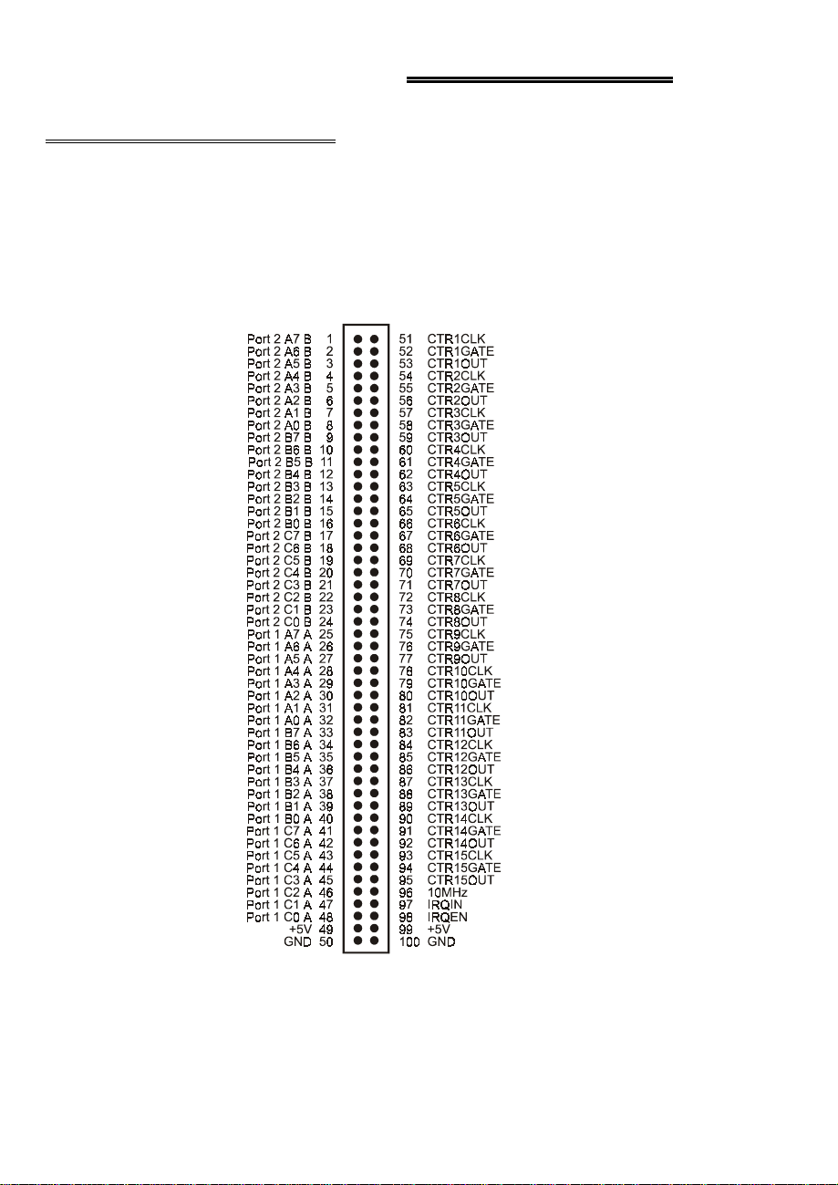
3 I/O CONNECTIONS
3.1 CONNECTOR DIAGRAM
The 100-pin, high-density connector is accessible through the computer’s expansion
bracket (Figure 3-1). The outputs signals from 8255 emulation registers are buffered
for higher current capacity. Three signals for each of the 15 82C54 counters, internal
PC +5V, and the 10 MHz oscillator output are also available.
Figure 3-1. 100-Pin Connector
3
Page 8
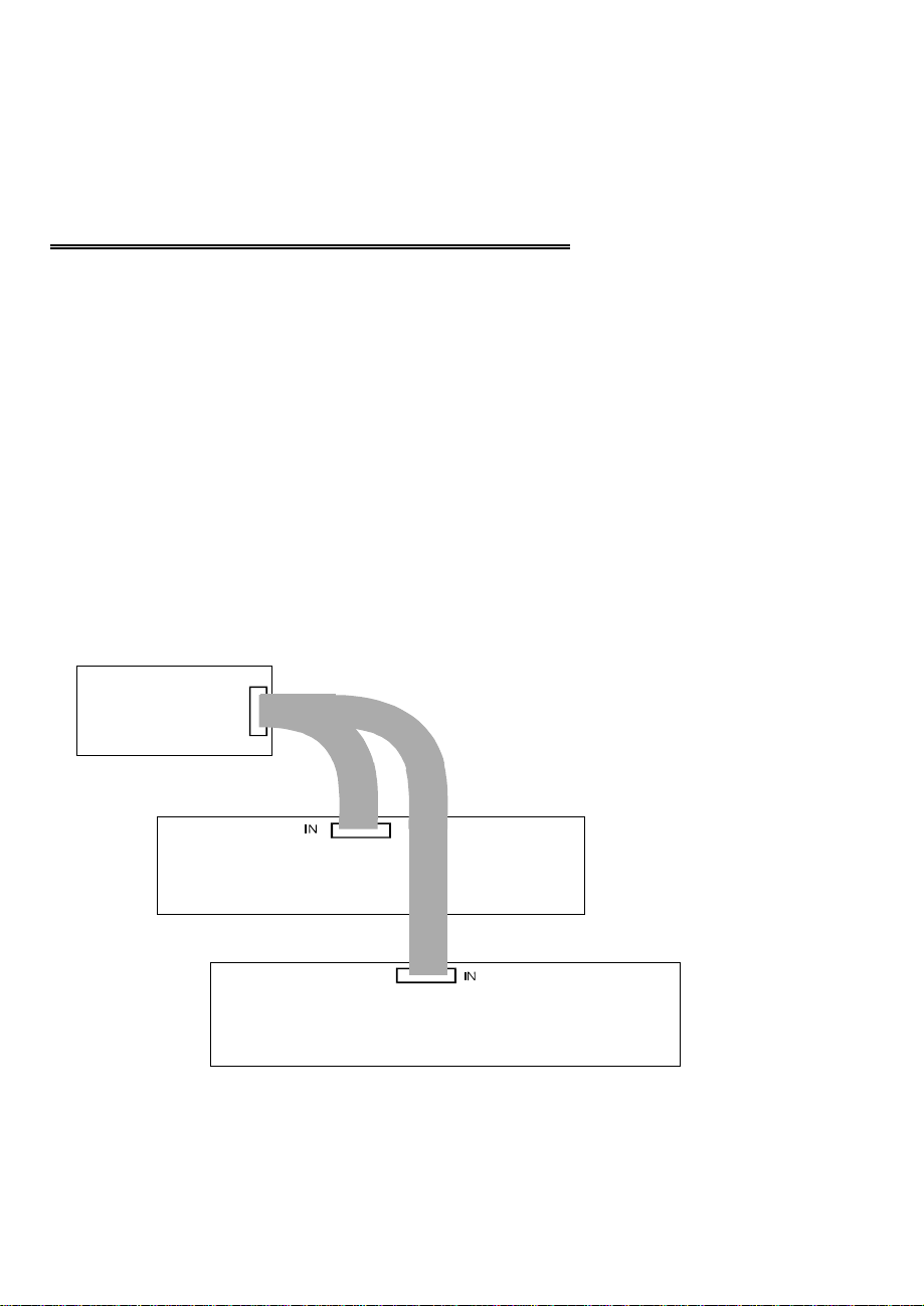
The I/O connections c an be brought o ut to easy-to-use screw terminals by purchasing
a CFF100-series cable and two CIO-MINI50 screw terminal boards. The 48 bits of
parallel digital I/O can be brought out to one of the CIO-MINI50s, and the
connections to the 15 counters would be brought out to the second.
As shown in Figure 3-2, the CFF100-xx cable has a 100-pin connector that fans out to
two, 50-pin cable legs.
3.2 SIGNAL CONNECTIONS & CONDITIONING
The 48 parallel digital I/O signals are buffered (high output drive) LSTTL. The
counter/timer signals are direct connections to the 82C54 chips and are CMOS TTL.
Refer to the Specification section for voltage and current ratings.
We offer a wide variety of digital signal conditioning products that provide an ideal
interface between high voltage or high current field signals and the
PCI-DIO48H/CTR15. If must control or monitor non-TTL level signals with your
board, please refer to our catalog or our web site for the following and other products.
CIO-ERB series, electromechanical relay output boards
CIO-SERB series, 10A electromechanical relay output boards
SSR-RACK series solid state I/O module racks
DR-Series, DIN rail mountable solid state I/O modules.
BOARD’S
100-PIN I/O
CONNECTOR
I/O PINS 1 TO 50
CONDITIONING or
50-PIN SCREW
TERMINAL BOARD.
C100FF-xx
CABLE
SIGNAL
I/O PINS 51 TO 100
SIGNAL CONDITIONING OR
50-PIN SCREW TERMINAL BOARD
Figure 3-2. C100FF-xx Cable Fan-out
4
Page 9
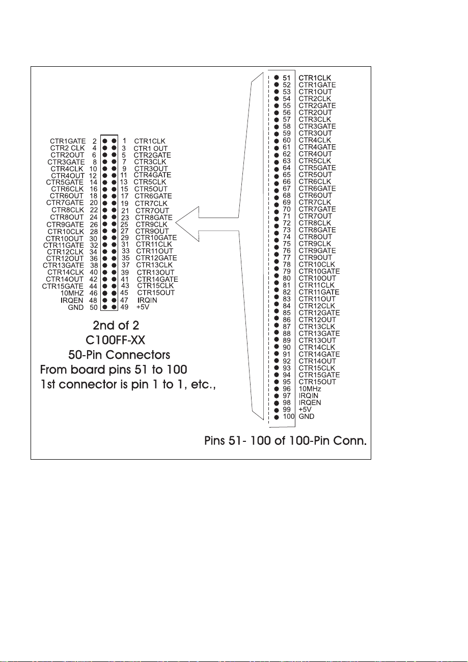
See Figure 3-3 for a translation diagram of the upper half (pins 51 to 100) of the
C100FF-xx cable to the second 50-pin connector.
Figure 3-3. C100FF-xx Pin-to-Pin Translation 51-100 to 1-50
IMPORTANT NOTE
This board emulates the 8255 chip. The 8255 emulation initializes all
ports as inputs on power-up and reset. These inputs typically w ill float
high and may have enough drive current to turn on any connected
devices.
If it is important that the outputs go to an OFF state (or an ON state) on a power-up or
reset, you must use pull-down resistors (or pull-up resistors for a mandatory ON
5
Page 10

state). We recommend using 2.2 K SIPs on the digital output pins. You will find
positions for pull up and pull down resistor packs on the board. For more details,
please refer to the application notes in Section 7.1 of this manual.
4 SOFTWARE
Due to the complex and somewhat unpredictable nature of Plug-and-Play addressing
software, we strongly recommend that users take advantage of our Universal Library
package's easy to use programming interfaces. However, if you are an experienced
programmer, and wish to read and write directly to the board, we have provided a
detailed register map in the next chapter.
4.1 UNIVERSAL LIBRARY
The Universal Library provides complete access to board functions from a range of
programming languages. If you are planning to write programs, or would like to run
the example progra ms for Visual Basic or any other language, ple ase consider using
Universal Library.
4.2 PACKAGED APPLICATION PROGRAMS
Most packaged application programs, such as SoftWIRE, DAS Wizard, and HP-VEE
have drivers for the PCI-DIO48H/CTR15. If the package you own does not appear to
have drivers for the boards, please fax or e-mail the package name and the revision
number from the install disks. We will research the package for you and advise how
to utilize the board with the driver available.
Some application drivers are included with the Universal Library package, but not
with the Application package. If you have purchased an application package directly
from the software vendor, you may need to purchase our Universal Library and
drivers. Please contact us for more information.
6
Page 11

5 I/O REGISTER MAPS
The PCI-DIO48H/CTR15 uses eight standard I/O addresses for the two 8255
emulations, 20 addresses for the five 82C54s (4 each) as well as the addresses
required for Plug-and-Play operation. The addresses are allocated by the PCI plug &
play procedure and may not be modified.
A word of warning: Direct writes to the addresses simply by reference to the base
address of the PCI-DIO48H/CTR15 I/O registers is not advised. Since the addresses
assigned by the PCI plug & play software are not under your control, there is no way
to guarantee that your program will run in any other computer. Not only that, but if
you install another PCI board in a computer after the PCI-DIO48H/CTR15 addresses
have been assigned, those addresses may be moved by the plug & play software when
the second board is installed. It is best to use a library such as Universal Library or a
application such as SoftWIRE to make measurements with your board.
Table 5-1. Board Registers
OPERATIONSWRITE FUNCTIONREAD FUNCTIONREGISTER
32-bit DWordInterrupt ControlInterrupt StatusBADR1 + 4Ch
8-bit ByteOutput Port 1A DataInput Port 1A DataBADR2 + 0h
8-bit ByteOutput Port 1B DataInput Port 1B DataBADR2 + 1
8-bit ByteOutput Port 1C DataInput Port 1C DataBADR2 + 2
8-bit ByteControl Register 1No ReadbackBADR2 + 3
8-bit ByteOutput Port 2A DataInput Port 2A DataBADR2 + 4
8-bit ByteOutput Port 2B DataInput Port 2B DataBADR2 + 5
8-bit ByteOutput Port 2C DataInput Port 2C DataBADR2 + 6
8-bit ByteControl Register 2No ReadbackBADR2 + 7
8-bit ByteCounter 1 DataCounter 1 DataBADR2 + 8
8-bit ByteCounter 2 DataCounter 2 DataBADR2 + 9
8-bit ByteCounter 3 DataCounter 3 DataBADR2 + A
8-bit ByteControl Counters 1-3No ReadbackBADR2 + B
8-bit ByteCounter 4 DataCounter 4 DataBADR2 + C
8-bit ByteCounter 5 DataCounter 5 DataBADR2 + D
8-bit ByteCounter 6 DataCounter 6 DataBADR2 + E
8-bit ByteControl Counters 4-6No ReadbackBADR2 + F
8-bit ByteCounter 7 DataCounter 7 DataBADR2 + 10h
8-bit ByteCounter 8 DataCounter 8 DataBADR2 + 11h
8-bit ByteCounter 9 DataCounter 9 DataBADR2 + 12h
8-bit ByteControl Counters 7-9No ReadbackBADR2 + 13h
8-bit ByteCounter 10 DataCounter 10 DataBADR2 + 14h
8-bit ByteCounter 11 DataCounter 11 DataBADR2 + 15h
8-bit ByteCounter 12 DataCounter 12 DataBADR2 + 16h
8-bit ByteControl Counters 10-12No ReadbackBADR2 + 17h
8-bit ByteCounter 13 DataCounter 13 DataBADR2 + 18h
8-bit ByteCounter 14 DataCounter 14 DataBADR2 + 19h
8-bit ByteCounter 15 DataCounter 15 DataBADR2 + 1Ah
8-bit ByteControl Counters 13-15No ReadbackBADR2 + 1Bh
7
Page 12

5.1 PCI-DIO48H/CTR15 REGISTER DESCRIPTION
INTERRUPT STATUS/CONTROL
BADR1 + 4Ch
READ/WRITE
0123456731:8
INTEINTPOLINTxxxxxx
This register, as with all the 9052 registers, is 32 bits long. Since the rest of the
register has specific control functions, they must be masked off when accessing the
interrupt control functions.
INTE Interrupt Enable
0 = disabled
1 = enabled (default).
INTPOL Interrupt Polarity
0 = active low (default)
1 = active high.
INT Interrupt Status
0 = interrupt is not active
1 = interrupt is active.
The digital I/O ports emulate 8255, Mode 0 operation.
PORT 1A DATA
BADR2 + 00h
READ/WRITE
PORT 1B DATA
BADR2 + 01h
READ/WRITE
PORT 1C DATA
BADR2 + 02h
READ/WRITE
01234567
A0A1A2A3A4A5A6A7
01234567
B0B1B2B3B4B5B6B7
01234567
CL0CL1CL2CL3CH0CH1CH2CH3
8
Page 13
CONTROL REGISTER 1
BADR2 + 03h
WRITE only
01234567
D0D1-D3D4---
The operating mode of the digital I/O ports is Mode 0. The control register therefore
is used to set the ports for inputs or outputs at the connector. For example, to set all
ports to output, write the value 0h to Base + 3. To set all p orts to input, write the
value 1Bh to Base + 3. The user can read the current state of an output port by simply
reading that port when configured to be output.
D7, D6, D5, and D2 are ‘don’t care’. They are shown as ‘0’ below. ‘CU’ is PORT C
upper nibble, ‘CL’ is PORT C lower nibble.
Table 5-2. DI/O Configuration Coding
DIO PORT VALUES CONTROL REG. CODES
CLCUBADecHexD0D1D3D4
OUTOUTOUTOUT000000
INOUTOUTOUT111000
OUTINOUTOUT220100
ININOUTOUT331100
OUTOUTINOUT880010
INOUTINOUT991010
OUTININOUT10A0110
INININOUT11B1110
OUTOUTOUTIN16100001
INOUTOUTIN17111001
OUTINOUTIN18120101
ININOUTIN19131101
OUTOUTININ24180011
INOUTININ25191011
OUTINININ261A0111
ININININ271B1111
PORT 2A DATA
BADR2 + 04h
READ/WRITE
PORT 2B DATA
BADR2 + 05h
READ/WRITE
01234567
A0A1A2A3A4A5A6A7
01234567
B0B1B2B3B4B5B6B7
9
Page 14

PORT 2C DATA
BADR2 + 06h
READ/WRITE
CONTROL REGISTER 2
BADR2 + 07h
WRITE only
See BADR2 + 03h and Table 5-2 for a description of the Control Register.
COUNTER 1 DATA
BADR2 + 08h
READ/WRITE
COUNTER 2 DATA
BADR2 + 09h
READ/WRITE
01234567
CL0CL1CL2CL3CH0CH1CH2CH3
01234567
D0D1-D3D4---
01234567
D0D1D2D3D4D5D6D7
01234567
D0D1D2D3D4D5D6D7
COUNTER 3 DATA
BADR2 + 0Ah
READ/WRITE
01234567
D0D1D2D3D4D5D6D7
CONTROL REGISTER COUNTERS 1 - 3
BADR2 + 0Bh
WRITE ONLY
01234567
D0D1D2D3D4D5D6D7
The control register is used to set the operating Modes of 8254 Counters 0,1 & 2. A
counter is configured by writing the correct Mode information to the Control
Register, then the proper count data must be written to the specific Counter Register.
The Counters on the 8254 are 16-bit devices. Since the interface to the 8254 is only
8-bits wide, Count data is written to the Counter Register as two successive bytes.
10
Page 15

First the low byte is written, then the high byte. The Control Register is 8-bits wide.
Further information can be obtained on the 82C54 data sheet, available from our web
site at www.measurementcomputing.com/82C54.
COUNTER 4 DATA
BADR2 + 0Ch
READ/WRITE
01234567
D0D1D2D3D4D5D6D7
COUNTER 5 DATA
BADR2 + 0Dh
READ/WRITE
01234567
D0D1D2D3D4D5D6D7
COUNTER 6 DATA
BADR2 + 0Eh
READ/WRITE
01234567
D0D1D2D3D4D5D6D7
CONTROL REGISTER COUNTERS 4 - 6
BADR2 + 0Fh
WRITE ONLY
01234567
D0D1D2D3D4D5D6D7
See BADR2 + 0Ch for full description of the Control Register.
COUNTER 7 DATA
BADR2 + 10h
READ/WRITE
COUNTER 8 DATA
BADR2 + 11h
READ/WRITE
11
01234567
D0D1D2D3D4D5D6D7
01234567
D0D1D2D3D4D5D6D7
Page 16

COUNTER 9 DATA
BADR2 + 12h
READ/WRITE
CONTROL REGISTER COUNTERS 7 - 9
BADR2 + 13h
WRITE ONLY
See BADR2 + 0Ch for full description of the Control Register.
COUNTER 10 DATA
BADR2 + 14h
READ/WRITE
COUNTER 11 DATA
BADR2 + 15h
READ/WRITE
01234567
D0D1D2D3D4D5D6D7
01234567
D0D1D2D3D4D5D6D7
01234567
D0D1D2D3D4D5D6D7
01234567
D0D1D2D3D4D5D6D7
COUNTER 12 DATA
BADR2 + 16h
READ/WRITE
CONTROL REGISTER COUNTERS 10 - 12
BADR2 + 17h
WRITE ONLY
See BADR2 + 0Ch for full description of the Control Register.
12
01234567
D0D1D2D3D4D5D6D7
01234567
D0D1D2D3D4D5D6D7
Page 17

COUNTER 13 DATA
BADR2 + 18h
READ/WRITE
COUNTER 14 DATA
BADR2 + 19h
READ/WRITE
COUNTER 15 DATA
BADR2 + 1Ah
READ/WRITE
CONTROL REGISTER COUNTERS 13 - 15
BADR2 + 1Bh
WRITE ONLY
01234567
D0D1D2D3D4D5D6D7
01234567
D0D1D2D3D4D5D6D7
01234567
D0D1D2D3D4D5D6D7
01234567
D0D1D2D3D4D5D6D7
See BADR2 + 0Ch for full description of the Control Register.
13
Page 18

6 SPECIFICATIONS
Typical for 25°C unless otherwise specified.
POWER CONSUMPTION
+5V Operating 1395 mA typical, 2091 mA max
DIGITAL INPUT/OUTPUT
Digital Type 8255 emulation, Mode 0
Output: 74S244
Input: 74LS373
Number of channels 48 I/O
Configuration 4 banks of 8, 4 banks of 4, programmable by
bank as input or output
Output High 2.4 volts min @ -15mA
Output Low 0.5 volts max @ 64 mA
Input High 2.0 volts min, 7 volts absolute max
Input Low 0.8 volts max, -0.5 volts absolute min
Power-up / reset state Input mode (high impedance)
Interrupts INTA# - mapped to IRQn via PCI BIOS at
boot-time, level sensitive - active low
Interrupt enable External enable (IRQEN), active low Internal
enable - programmable enable/disable through
PCI9052 (enabled by default)
Interrupt sources External source (IRQIN), polarity programmable
through PCI9052 (active low by default)
COUNTER SECTION
Counter type 82C54
Configuration 15 down-counters per 82C54, 16 bits each
82C54A:
Counter 0 - User counter #1
Source: Available at user connector (CTR1CLK)
Gate: Available at user connector (CTR1GATE)
Output: Available at user connector (CTR1OUT)
Counter 1 - User counter #2
Source: Available at user connector (CTR2CLK)
Gate: Available at user connector (CTR2GATE)
Output: Available at user connector (CTR2OUT)
Counter 2 - User counter #3
Source: Available at user connector (CTR3CLK)
Gate: Available at user connector (CTR3GATE)
Output: Available at user connector (CTR3OUT)
14
Page 19

82C54B:
Counter 0 - User counter #4
Source: Available at user connector (CTR4CLK)
Gate: Available at user connector (CTR4GATE)
Output: Available at user connector (CTR4OUT)
Counter 1 - User counter #5
Source: Available at user connector (CTR5CLK)
Gate: Available at user connector (CTR5GATE)
Output: Available at user connector (CTR5OUT)
Counter 2 - User counter #6
Source: Available at user connector (CTR6CLK)
Gate: Available at user connector (CTR6GATE)
Output: Available at user connector (CTR6OUT)
82C54C:
Counter 0 - User counter #7
Source: Available at user connector (CTR7CLK)
Gate: Available at user connector (CTR7GATE)
Output: Available at user connector (CTR7OUT)
Counter 1 - User counter #8
Source: Available at user connector (CTR8CLK)
Gate: Available at user connector (CTR8GATE)
Output: Available at user connector (CTR8OUT)
Counter 2 - User counter #9
Source: Available at user connector (CTR9CLK)
Gate: Available at user connector (CTR9GATE)
Output: Available at user connector (CTR9OUT)
82C54D:
Counter 0 - User counter #10
Source: Available at user connector (CTR10CLK)
Gate: Available at user connector (CTR10GATE)
Output: Available at user connector (CTR10OUT)
Counter 1 - User counter #11
Source: Available at user connector (CTR11CLK)
Gate: Available at user connector (CTR11GATE)
Output: Available at user connector (CTR11OUT)
Counter 2 - User counter #12
Source: Available at user connector (CTR12CLK)
Gate: Available at user connector (CTR12GATE)
Output: Available at user connector (CTR12OUT)
82C54E:
Counter 0 - User counter #13
Source: Available at user connector (CTR13CLK)
Gate: Available at user connector (CTR13GATE)
Output: Available at user connector (CTR13OUT)
15
Page 20

Counter 1 - User counter #14
Source: Available at user connector (CTR14CLK)
Gate: Available at user connector (CTR14GATE)
Output: Available at user connector (CTR14OUT)
Counter 2 - User counter #15
Source: Available at user connector (CTR15CLK)
Gate: Available at user connector (CTR15GATE)
Output: Available at user connector (CTR15OUT)
Clock input frequency 10 MHz max
High pulse width (clock input) 30 ns min
Low pulse width (clock input) 50 ns min
Gate width high 50 ns min
Gate width low 50 ns min
Input low voltage 0.8V max
Input high voltage 2.0V min
Output low voltage 0.4V max
Output high voltage 3.0V min
Crystal oscillator clock source 10 MHz, output available at user connector
(10MHz)
Frequency accuracy 50 ppm
ENVIRONMENTAL
Operating temperature range 0 to 50°C
Storage temperature range -20 to 70°C
Humidity 0 to 90% non-condensing
16
Page 21

7 ELECTRONICS AND INTERFACING
This short introduction to the electronics, most often needed by digital I/O board
users, covers a few key concepts.
IMPORTANT NOTE
WHENEVER THE 8255 (or its emulation) IS POWERED- ON OR
RESET, ALL PINS ARE SET TO HIGH IMPEDANCE INPUT.
The implications of this is that if you have output devices such as solid state relays,
they may be switched on whenever the computer is powered on or reset. To prevent
unwanted switching and to drive all outputs to a known (safe) state after power-on or
reset, pull all pins either high or low through a 2.2K resistor.
7.1 PULL UP & PULL DOWN RESISTORS
Whenever board is powered on or reset, the digital I/O control registers are set to a
known state. That state is mode 0, all ports input. The input bits are of the 74LS
series and will typically (but not certainly) float high when in the input mode. There
may also be enough drive current available from the inputs to turn on connected
devices.
If the inputs of the device you are controlling are left to float, they may float up or
down. Which way they float is dependent on the characteristics of the circuit and the
electrical environment; and may be unpredictable. The result is that your controlled
device may get turned on. That is why you need pull up or pull down resistors.
Shown here is one digital output with a
pull-up resistor attached.
The pull-up resistor provides a
reference to +5V while its value of
2200 ohms requires only 2.3 mA of
drive current
Digital
Output
Circuit
If the board is reset and enters high
impedance input, the line is pulled
high. At that point, both the board
AND the device being controlled will
sense a high signal.
Figure 7-1. Pull-Up Resistor Schematic
If the board is in output mode , it has more than enough power (64 mA) to over ride
the pull-up/down resistor's high signal and drive the line to 0 volts.
17
Page 22

Of course, a pull-down resistor accomplishes the same task except that the line is
pulled low when the board is reset and the output has more than enough power to
drive the line high.
The PCI-DIO48H/CTR15 is equipped with positions for pull-up/down resistor Single
Inline Packages (SIPs). The positions are marked PORT 0 A, B and C and PORT1 A,
B and C and are located beside the I/O connector.
A 2.2K, eight-resistor SIP is made of eight, 2.2K resistors all connected to a single
common point and the other pins protruding from the SIP. The common pin at one
end of the SIP is marked with a dot.
The SIP can be installed to pull-up or pull-down. At each location, A, B & C on the
PCI-DIO48H/CTR15 series boards, there are 10 holes in a line. One end of the line
is +5V, the other end is GND. They are marked HI and LO. The eight holes in
between are connected to the eight lines of the port, A, B, or C.
To implement a pull-up, insert the SIP with the common end in the HI hole. To do an
eight-input pull-down, insert the SIP’s common pin in the LO hole.
A resistor value of 2.2K is recommended. Use other values only if you have
calculated the necessity of doing so.
REMEMBER, UNCONNECTED INPUTS FLOAT!
Keep in mind that unconnected inputs typically f loat high. If you are
using the board for input, and have unconnected inputs, ignore the data
from those lines.
In other words, if you connect bit A0 and not bit A1, do not be surp rised if A1 stays
low, stays high, or tracks A0... It is unconnected, and so, is unspecified.
You do not have to pull up or pull down input lines since unconnected lines will not
affect the performance of connected lines. Just make sure to mask out any
unconnected bits in software.
7.2 TTL TO SOLID STATE RELAYS
Many applications require digital outputs to switch high AC and DC voltages on and
off and to monitor high AC and DC voltages. Ob viously, these high voltage s cannot
be controlled or read directly by the TTL digital lines of a PCI-DIO48H/CTR15.
Solid State Relays, such as those available from Computer Boards, Inc. allow control
and monitoring of AC and high DC voltages and provide 750V isolation. Solid State
Relays (SSRs) are the recommended method of interfacing to AC and high DC
signals.
The most convenient way to use solid state relays and a PCI-DIO48H/CTR15 board
is to purchase a Solid State Relay Rack. A SSR Rack is a circuit board with output
buffer chips which are powerful eno ugh to switch the SSR and sockets to plug SSRs
into. SSR Racks are available from Computer Boards and most manufacturers of
18
Page 23

SSRs. If you have only a few outputs to control, you may also wish to consider the
DR-OAC or DR-ODC, single point, DIN mountable SSRs. The high current o utputs
of the PCI-DIO48H/CTR15 board are suitable to drive these SSRs directly.
7.3 VOLTAGE DIVIDERS
If you need to detect a signal which varies over a range greater than the maximum
input specification of a digital input, you must use a voltage divider or some other
external device to reduce the voltage of the input signal to a safe level.
Ohm's law states,
Voltage = Current * Resistance
Implied in the above is that any variation in the voltage drop for the circuit as a whole
will have a proportional variation
in all the voltage drops in the
circuit.
In a voltage divider, the voltage
across one of the resistors in a
circuit is proportional to the
resistance to the total resistance in
the circuit.
The object in using a voltage
divider is to choose two resistors
with the proper proportions relative
to the full value of the input voltage
to the desired output voltage to the
board input (Figure 7-2).
Signal
High
Signal
Vin
Volts
Signal
Low
SIMPLE VOLTAGE DI VIDER - Vin = R1+R2
R1
R2
Vout R2
V1
V2
Vout
Board
Input
Groundt
Figure 7-2. Voltage Divider Schematic
Dropping the voltage proportionally is called attenuation. The formula for
attenuation is:
The variable Attenuation is the
Attenuation = R1+R2
R2
proportional difference between the
desired output voltage (max. input
board input voltage) and the full input
voltage from the field device.
For example, if the field voltage varies
2 = 10K+10K
10K
between 0 and 10 volts and you wish to
detect that with a maximum board input
voltage of 5 volts, the Attenuation must
be 2:1 or simply 2.
19
Page 24

For a given attenuation, pick a handy
R1 = (A−1) x R2
Digital inputs often require voltage dividers. For example, if you wish to detect a field
signal that is at 0 volts when OFF and 24 volts when ON, you cannot connect that
directly to the PCI-DIO48H/CTR15 digital inputs. The voltage must be dropped to
5 volts maximum when ON. The Attenuation required is 24:5 or 4.8. Use the
equation above to find an appropriate R1 if R2 is 1K. Remember that a TTL input is
'ON' when the input voltage is greater than 2.5 volts.
The resistors, R1 and R2, are going to dissipate all the power in the
divider circuit according to the equation,
Current = Voltage / Resistance. The higher the value of the resistance (R1 + R2) the
less power dissipated by the divider circuit. As a simple rule:
For Attenuation of 5:1 or less, no resistor should be less than 10K.
For Attenuation of greater than 5:1, no resistor should be less than 1K.
resistor and call it R2, then use this
formula to calculate R1.
NOTE
20
Page 25

For your notes
21
Page 26

For Your Notes
22
Page 27

EC Declaration of Conformity
We, Measurement Computing Corporation, declare under sole responsibility that the
product:
Digital I/O board with 15 countersPCI-DIO48H/CTR15
DescriptionPart Number
to which this declaration relates, meets the essential requirements, is in conformity
with, and CE marking has been applied according to the relevant EC Directives listed
below using the relevant section o f the following EC standards and other no rmative
documents:
EU EMC Directive 89/336/EEC: Essential requirements relating to electromagnetic
compatibility.
EU 55022 Class B: Limits and methods of measurements of radio interference
characteristics of information technology equipment.
EN 50082-1: EC generic immunity requirements.
IEC 801-2: Electrostatic discharge requirements for industrial process measurement
and control equipment.
IEC 801-3: Radiated electromagnetic field requirements for industrial process
measurements and control equipment.
IEC 801-4: Electrically fast transients for industrial process measurement and control
equipment.
Carl Haapaoja, Director of Quality Assurance
Page 28

Measurement Computing Corporation
16 Commerce Boulevard,
Middleboro, Massachusetts 02346
(508) 946-5100
Fax: (508) 946-9500
E-mail: info@measurementcomputing.com
www.measurementcomputing.com
 Loading...