

Page 1

PCI-DDA02/12
Document Revision 3
March 2012
© Copyright 2012
User's Guide
Analog Output and Digital I/O
Page 2

HM PCI-DDA02-12.docx
Your new Measurement Computing product comes with a fantastic extra —
Management committed to your satisfaction!
Thank you for choosing a Measurement Computing product—and congratulations! You own the finest, and you can now enjoy
the protection of the most comprehensive warranties and unmatched phone tech support. It’s the embodiment of our mission:
To provide data acquisition hardware and software that will save time and save money.
Simple installations minimize the time between setting up your system and actually making measurements. We offer quick and
simple access to outstanding live FREE technical support to help integrate MCC products into a DAQ system.
Limited Lifetime Warranty: Most MCC products are covered by a limited lifetime warranty against defects in materials or
workmanship for the life of the product, to the original purchaser, unless otherwise noted. Any products found to be defective in
material or workmanship will be repaired, replaced with same or similar device, or refunded at MCC’s discretion. For specific
information, please refer to the terms and conditions of sale.
Harsh Environment Program: Any Measurement Computing product that is damaged due to misuse, or any reason, may be
eligible for replacement with the same or similar device for 50% of the current list price. I/O boards face some harsh
environments, some harsher than the boards are designed to withstand. Contact MCC to determine your product’s eligibility for
this program.
30 Day Money-Back Guarantee: Any Measurement Computing Corporation product may be returned within 30 days of
purchase for a full refund of the price paid for the product being returned. If you are not satisfied, or chose the wrong product by
mistake, you do not have to keep it.
These warranties are in lieu of all other warranties, expressed or implied, including any implied warranty of merchantability or
fitness for a particular application. The remedies provided herein are the buyer’s sole and exclusive remedies. Neither
Measurement Computing Corporation, nor its employees shall be liable for any direct or indirect, special, incidental or
consequential damage arising from the use of its products, even if Measurement Computing Corporation has been notified in
advance of the possibility of such damages.
Trademark and Copyright Information
Measurement Computing Corporation, InstaCal, Universal Library, and the Measurement Computing logo are either trademarks
or registered trademarks of Measurement Computing Corporation. Refer to the Copyrights & Trademarks section on
mccdaq.com/legal for more information about Measurement Computing trademarks. Other product and company names
mentioned herein are trademarks or trade names of their respective companies.
© 2012 Measurement Computing Corporation. All rights reserved. No part of this publication may be reproduced, stored in a
retrieval system, or transmitted, in any form by any means, electronic, mechanical, by photocopying, recording, or otherwise
without the prior written permission of Measurement Computing Corporation.
Notice
Measurement Computing Corporation does not authorize any Measurement Computing Corporation product for use
in life support systems and/or devices without prior written consent from Measurement Computing Corporation.
Life support devices/systems are devices or systems that, a) are intended for surgical implantation into the body, or
b) support or sustain life and whose failure to perform can be reasonably expected to result in injury. Measurement
Computing Corporation products are not designed with the components required, and are not subject to the testing
required to ensure a level of reliability suitable for the treatment and diagnosis of people.
Page 3

Table of Contents
Preface
About this User's Guide ....................................................................................................................... 4
What you will learn from this user's guide ......................................................................................................... 4
Conventions in this user's guide ......................................................................................................................... 4
Where to find more information ......................................................................................................................... 4
Register-level programming ............................................................................................................................................. 4
Chapter 1
Introducing the PCI-DDA02/12 ............................................................................................................. 5
Functional block diagram ................................................................................................................................... 5
Chapter 2
Installing the PCI-DDA02/12 ................................................................................................................. 6
What comes with your shipment? ....................................................................................................................... 6
Hardware .......................................................................................................................................................................... 6
Software ............................................................................................................................................................................ 6
Documentation ................................ ................................................................ ................................................................ .. 6
Optional components ........................................................................................................................................................ 6
Unpacking........................................................................................................................................................... 6
Installing the software ........................................................................................................................................ 6
Installing the hardware ....................................................................................................................................... 6
Signal connections .............................................................................................................................................. 7
Signal termination ............................................................................................................................................................. 9
Chapter 3
Functional Details ............................................................................................................................... 10
Analog connections .......................................................................................................................................... 10
Digital connections ........................................................................................................................................... 10
Pull up and pull down resistors ........................................................................................................................................10
Chapter 4
Calibrating the PCI-DDA02/12 ............................................................................................................ 12
Self-calibrating ................................................................................................................................................. 12
Calibration configuration .................................................................................................................................. 12
"In-system" calibration ..................................................................................................................................... 13
Chapter 5
Specifications ...................................................................................................................................... 14
Power consumption .......................................................................................................................................... 14
Analog output ................................................................................................................................................... 14
Digital input / output ......................................................................................................................................... 15
Environmental .................................................................................................................................................. 15
Main connector and pinout ............................................................................................................................... 15
Declaration of Conformity .................................................................................................................. 17
3
Page 4

About this User's Guide
What you will learn from this user's guide
This user's guide describes the Measurement Computing PCI-DDA02/12 data acquisition device and lists
device specifications.
Conventions in this user's guide
For more information
Text presented in a box signifies additional information and helpful hints related to the subject matter you are
reading.
Caution! Shaded caution statements present information to help you avoid injuring yourself and others,
damaging your hardware, or losing your data.
bold text Bold text is used for the names of objects on a screen, such as buttons, text boxes, and check boxes.
italic text Italic text is used for the names of manuals and help topic titles, and to emphasize a word or phrase.
Where to find more information
Additional information about the PCI-DDA02/12 is available on our website at www.mccdaq.com. You can
also contact Measurement Computing Corporation by phone, fax, or email with specific questions.
Preface
Phone: 508-946-5100 and follow the instructions for reaching Tech Support
Fax: 508-946-9500 to the attention of Tech Support
Email: techsupport@mccdaq.com
Register-level programming
You should use the Universal Library to control your board. Only experienced programmers should attempt
register-level programming. If you need to program at the register level in your application, refer to the Register
Map for the PCI-DDA0x/12 Series on our web site at www.mccdaq.com/registermaps/RegMapPCI-DDA0x-
12.pdf.
4
Page 5
Chapter 1
Introducing the PCI-DDA02/12
The PCI-DDA02/12 provides two channels of 12-bit analog output and 48-bits of digital I/O.
The D/A converters can be independently configured for either Bipolar or Unipolar. Bipolar ranges are ±10 V,
±5 V, and ±2.5 V. Unipolar ranges are 0 to 10 V, 0 to 5 V, and 0 to 2.5 V. The outputs may be updated
individually or simultaneously. The range settings are software-selectable.
The digital I/O ports are configured as two 82C55 mode 0 emulations. Each group is divided into three 8-bit
ports — Port A, Port B, and Port C. Port C can be split into two four-bit ports — Port C-HI and Port C-LO.
Each of these ports may be individually programmed as input or output. The digital outputs are capable of
sinking 64 mA and sourcing 15 mA utilizing standard "S" logic.
The PCI interface uses the PLX 9052 chip, which is a slave-only device. The PCI interface for the analog output
is configured in a 16-bit, multiplexed address/data bus, I/O access mode. The PCI interface for the digital I/O is
configured in an 8-bit, multiplexed address/data bus, I/O access mode to be register-compatible with the PCIDIO48H and PCI-DIO96H boards.
The PCI-DDA02/12 board is completely plug-and-play, with no jumpers or switches to set. All board addresses
are set by the board's plug-and-play software. Board configuration is controlled by your system's BIOS.
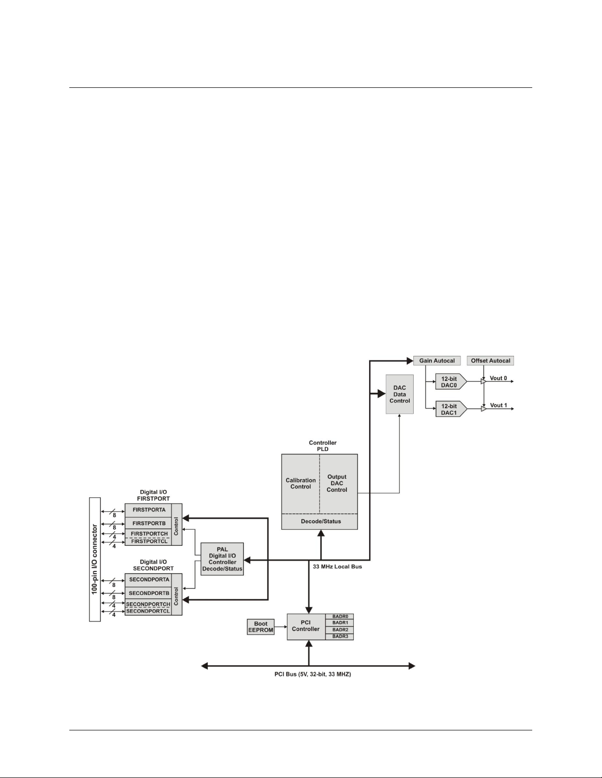
Functional block diagram
PCI-DDA02/12 functions are illustrated in the block diagram shown here.
Figure 1. PCI-DDA02/12 functional block diagram
5
Page 6

Chapter 2
Installing the PCI-DDA02/12
What comes with your shipment?
Verify that the following components are included in the shipment:
Hardware
PCI-DDA02/12
Software
MCC DAQ CD
Documentation
In addition to this hardware user's guide, you should also receive the Quick Start Guide. This booklet provides
an overview of the MCC DAQ software you received with the device, and includes information about installing
the software. Please read this booklet completely before installing any software or hardware.
Optional components
C100FF-x cable
Signal termination boards
Measurement Computing provides signal termination boards for use with the PCI-DDA02/12. Refer to
Signal termination on page 9 for more information.
Unpacking
As with any electronic device, you should take care while handling to avoid damage from static
electricity. Before removing the PCI-DDA02/12 from its packaging, ground yourself using a wrist strap or by
simply touching the computer chassis or other grounded object to eliminate any stored static charge.
If any components are missing or damaged, notify Measurement Computing Corporation immediately by
phone, fax, or e-mail:
Phone: 508-946-5100 and follow the instructions for reaching Tech Support
Fax: 508-946-9500 to the attention of Tech Support
Email: techsupport@mccdaq.com
For international customers, contact your local distributor. Refer to the International Distributors section on our
web site at www.mccdaq.com/International.
Installing the software
Refer to the Quick Start Guide for instructions on installing the software on the MCC DAQ CD. This booklet is
available in PDF at www.mccdaq.com/PDFmanuals/DAQ-Software-Quick-Start.pdf.
Installing the hardware
The PCI-DDA02/12 board is completely plug-and-play. There are no switches or jumpers to set. Configuration
is controlled by your system's BIOS.
Install the MCC DAQ software before you install your board
The driver needed to run your board is installed with the MCC DAQ software. Therefore, you need to install the
MCC DAQ software before you install your board. Refer to the Quick Start Guide for instructions on installing
the software.
6
Page 7

PCI-DDA02/12 User's Guide Installing the PCI-DDA02/12
Connector type
100-pin, high density connector
Compatible cables
C100FF-x unshielded ribbon cable (x = length in feet)
Compatible accessory products with
the C100FF-x cable
SCB-50
CIO-TERM100
CIO-MINI50 (two required)
Complete the following steps to install the board:
1. Turn your computer off, open it up, and insert your board into an available PCI slot.
2. Close your computer and turn it on.
When you connect the device for the first time to a computer running Windows, a Found New Hardware
dialog opens when the operating system detects the device. If the information file for this board is not
already loaded onto your PC, you will be prompted for the disk containing this file. The MCC DAQ
software contains this file. If required, insert the Measurement Computing Data Acquisition Software CD
and click OK.
3. To test your installation and configure your board, run the InstaCal utility you installed in the previous
section. Refer to the Quick Start Guide that came with your board www.mccdaq.com/PDFmanuals/DAQ-
Software-Quick-Start.pdf for information on how to initially set up and load InstaCal.
Signal connections
The table below lists the board connectors, applicable cables and compatible accessory boards.
7
Page 8

PCI-DDA02/12 User's Guide Installing the PCI-DDA02/12
Signal name
Pin Pin
Signal name
Digital Ground
100
50
Digital Ground
+5V
99
49
NC
FIRSTPORTC Bit 0
98
48
NC
FIRSTPORTC Bit 1
97
47
NC
FIRSTPORTC Bit 2
96
46
NC
FIRSTPORTC Bit 3
95
45
NC
FIRSTPORTC Bit 4
94
44
NC
FIRSTPORTC Bit 5
93
43
NC
FIRSTPORTC Bit 6
92
42
NC
FIRSTPORTC Bit 7
91
41
NC
FIRSTPORTB Bit 0
90
40
NC
FIRSTPORTB Bit 1
89
39
NC
FIRSTPORTB Bit 2
88
38
NC
FIRSTPORTB Bit 3
87
37
NC
FIRSTPORTB Bit 4
86
36
NC
FIRSTPORTB Bit 5
85
35
NC
FIRSTPORTB Bit 6
84
34
NC
FIRSTPORTB Bit 7
83
33
NC
FIRSTPORTA Bit 0
82
32
NC
FIRSTPORTA Bit 1
81
31
NC
FIRSTPORTA Bit 2
80
30
NC
FIRSTPORTA Bit 3
79
29
NC
FIRSTPORTA Bit 4
78
28
NC
FIRSTPORTA Bit 5
77
27
NC
FIRSTPORTA Bit 6
76
26
NC
FIRSTPORTA Bit 7
75
25
NC
SECONDPORTC Bit 0
74
24
NC
SECONDPORTC Bit 1
73
23
NC
SECONDPORTC Bit 2
72
22
NC
SECONDPORTC Bit 3
71
21
NC
SECONDPORTC Bit 4
70
20
NC
SECONDPORTC Bit 5
69
19
NC
SECONDPORTC Bit 6
68
18
NC
SECONDPORTC Bit 7
67
17
NC
SECONDPORTB Bit 0
66
16
NC
SECONDPORTB Bit 1
65
15
NC
SECONDPORTB Bit 2
64
14
NC
SECONDPORTB Bit 3
63
13
NC
SECONDPORTB Bit 4
62
12
NC
SECONDPORTB Bit 5
61
11
NC
SECONDPORTB Bit 6
60
10
NC
SECONDPORTB Bit 7
59
9
NC
SECONDPORTA Bit 0
58
8
Analog Ground
SECONDPORTA Bit 1
57
7
NC
SECONDPORTA Bit 2
56
6
Analog Ground
SECONDPORTA Bit 3
55
5
NC
SECONDPORTA Bit 4
54
4
Analog Ground
SECONDPORTA Bit 5
53
3
Vout 1
SECONDPORTA Bit 6
52
2
Analog Ground
SECONDPORTA Bit 7
51
1
Vout 0
PCI slot ↓
The PCI-DDA02/12 uses a single 100-pin high density connector on the back plate of the board to bring out all
required digital and analog lines and grounds.
I/O connector pinout
8
Page 9

PCI-DDA02/12 User's Guide Installing the PCI-DDA02/12
Figure 2. C100FF-x cable
Details on the C100FF-x cable are available on our web site at www.mccdaq.com/products/accessories.aspx.
Information on signal connections
General information regarding signal connection and configuration is available in the Guide to Signal
Connections. This document is available on our web site at www.mccdaq.com/signals/signals.pdf.
Signal termination
You can use the following screw terminal boards with the C100FF-x cable:
SCB-50: 50 conductor, shielded signal connection/screw terminal box; provides two independent 50-pin
connections, with each connected one-to-one to a 50-pin header for ribbon cable mating.
CIO-TERM100: 100-pin screw terminal board with daisy-chained 50-pin IDC connectors.
CIO-MINI50: 50-pin screw terminal board.
Details on these products are available on our web site at www.mccdaq.com/products/screw_terminal_bnc.aspx.
9
Page 10

Chapter 3
Functional Details
Analog connections
The analog output connections on the PCI-DDA02/12 series are two-wire hookups. One wire connects to the
signal labeled Vout #, where # is the channel number from 0 to 1. The other wire connects to the associated
analog ground. The I/O connector pinout is shown on page 8.
Analog ranges are software-selectable for ±10 V, ±5 V, ±2.5 V, 0 to 10 V, 0 to 5 V, and 0 to 2.5 V. Each port
may be reconfigured easily and quickly.
Digital connections
The PCI-DDA02/12 emulates two 82C55 chips, but offers much higher drive capability than the 82C55. The
board emulates only Mode 0 of the 82C55 (no strobed I/O or bi-directional I/O bits). The PCI-DDA02/12 is
completely plug-and-play, without any onboard user configurable switches or jumpers. The 48 CMOS/TTL
compatible digital I/O lines are configured in four banks of eight and four banks of four. You can configure
each bank for input or output.
All of the digital outputs/inputs on the PCI-DDA02/12 connector are TTL-compatible. TTL is an electronics
industry term, short for Transistor Transistor Logic, a standard for digital signals which are either at near 0V or
near 5V. The outputs are capable of sinking 64 mA or sourcing 15 mA. All I/O is brought out to the 100-pin
connector, which also allows connection to the computer's +5 volt and ground.
Unconnected inputs float
Unconnected inputs typically float high, but not reliably. If you are using a PCI-DDA02/12 board for input and
have unconnected inputs, ignore the data from those lines. You do not have to terminate input lines.
Unconnected lines will not affect the performance of connected lines. Ensure that you mask out any
unconnected bits in software.
Pull up and pull down resistors
Whenever the board is powered-on or reset, all ports are set to input mode. To drive all outputs to a known state
after power on or reset, pull all pins either high or low through a 2.2 kΩ resistor.
The pull-up resistor pulls the input to a high state (+5V). Its resistance of 2200 Ω draws only 2 mA of the
64 mA available from the output.
A 2200 Ω pull-down resistor does the same task, except that the line is pulled low when the board is in the
input mode, and uses only 2 mA of the 15 mA available output provided by the board.
The PCI-DDA02/12 board has open positions for up to six Single Inline Package (SIPs) resistors. The locations
are marked Port 0A, 0B, and 0C, and Port 1A, 1B, and 1C, and are adjacent to the I/O connector. Port 0n
corresponds to FIRSTPORTn, and Port 1n corresponds to SECONDPORTn.
The SIP resistors provide either pull-up or pull-down action for each eight-line port, depending on their
orientation in the port positions on the board.
The SIP is made up of eight 2.2 kΩ resistors. One side of each resistor is connected to a single common point
and brought out to a pin. The common line is marked with a dot or line at one end of the SIP. The remaining
resistor ends are brought out to the other eight pins (refer to Figure 3).
10
Page 11

PCI-DDA02/12 User's Guide Functional Details
Figure 3. Eight-Resistor SIP Schematic
You can install the SIP as either pull-up or pull-down. At each location there are 10 holes in a line. One end of
the line is +5V, the other end is GND. They are marked HI and LO respectively. The eight holes in the middle
are connected to the eight lines of a port.
For a pull-up function per port, mount the SIP with the common pin (marked with a dot or line) in the HI
position.
For a pull-down function per port, mount the SIP with the common pin in the LO position.
When installing pull-up and pull-down resistor SIP packs, we recommend using a 2.2 K, eight-resistor SIP
(MCC part number SP-K2.29C). You can substitute individual 2.2 kΩ resistors for the resistor SIPs, if required.
11
Page 12

Chapter 4
Calibrating the PCI-DDA02/12
Self-calibrating
The PCI-DDA02/12 is shipped fully-calibrated from the factory. Calibration coefficients are stored in
nonvolatile RAM. When using the Universal Library, the calibration factors are read from nonvolatile RAM
and are automatically written to the calibration DACs each time you select a different DAC range.
Use InstaCal to recalibrate with respect to the factory-measured voltage standards. InstaCal calibrates each
channel at all six ranges. Each channel takes less than a minute to calibrate.
Calibration configuration
The PCI-DDA02/12 provides self-calibration of the analog source and measure systems. This eliminates the
need for external equipment and user adjustments. The analog output circuits are calibrated for both gain and
offset. Gain calibration of the analog output is performed via DAC reference adjustments. Offset adjustments
for the analog output is made in the output buffer section.
PCI-DDA02/12 calibration circuitry is shown in Figure 4.
Figure 4. Calibration block diagram
12
Page 13

PCI-DDA02/12 User's Guide Calibrating the PCI-DDA02/12
"In-system" calibration
The PCI-DDA02/12 is calibrated at the factory for the correct voltages at the I/O connector. For more precise
application of voltages at the "system end", we can provide a version of InstaCal that allows you to calibrate the
board within your system for correct voltages at your field connection. This calibration lets you remove the
effects of voltage drops caused by IR loss in the cable and connector for resistances up to 1 Ω. This calibration
also allows you to zero out errors in any external signal conditioning up to approximately ±10 mV.
In most applications, the version of InstaCal that ships with the board provides the accuracy specified. If your
application has unusual requirements, such as long cables, you may need the "in-system version" to achieve this
accuracy.
Contact technical support by phone, fax, or e-mail for details regarding the "in-system" calibration feature.
Phone: 508-946-5100 and follow the instructions for reaching Tech Support
Fax: 508-946-9500 to the attention of Tech Support
Email: techsupport@mccdaq.com
For international customers, contact your local distributor. Refer to the International Distributors section on our
web site at www.mccdaq.com/International.
13
Page 14

Specifications
+5 V operating
1.4 A typical, 2.2 A max
+12 V
6 mA typical, 12 mA max
-12 V
4 mA typical, 6 mA max
D/A converter type
AD7837B
Resolution
12-bits
Number of channels
2
Output ranges
±10 V, ±5 V, ±2.5 V, 0 to 10 V, 0 to 5 V, 0 to 2.5 V.
Each channel independently programmable.
Data transfer
Programmed I/O
Offset error (calibrated)
±(300 µV + ¼ LSB)
Gain error (calibrated)
±(300 µV + ¼ LSB)
Differential nonlinearity
±1 LSB max
Integral nonlinearity
±1 LSB max
Monotonicity
12-bits
D/A gain drift
±2 ppm/°C
D/A offset drift
±5 µV/°C
Throughput
PC dependent
Settling time (20V step to ±½LSB)
6 µs typ, 10µs max
Slew rate
5 V/µs
Current drive
±5 mA
Output short-circuit duration
25 mA indefinite
Output coupling
DC
Output impedance
0.1 Ohms max
Miscellaneous
Double buffered output latches
Update DACs individually or simultaneously (software selectable)
Power up and reset, all DAC's cleared to 0 volts, ±210 mV
Typical for 25 °C unless otherwise specified.
Specifications in italic text are guaranteed by design.
Power consumption
Table 1. Power consumption specifications
Analog output
Table 2. Analog output specifications
Chapter 5
14
Page 15

PCI-DDA02/12 User's Guide Specifications
Digital type (main connector)
82C55 mode 0 emulation
Output: 74S244
Input: 74LS373
Configuration
4 banks of 8, 4 banks of 4, programmable by bank as input or output
Number of channels
48 I/O
Output high
2.4 volts min @ -15 mA
Output low
0.5 volts max @ 64 mA
Input high
2.0 volts min, 7 volts absolute max
Input low
0.8 volts max, -0.5 volts absolute min
Power-up / reset state
Input mode (high impedance)
Operating temperature range
0 to 70 °C
Storage temperature range
-40 to 100 °C
Humidity
0 to 90% non-condensing
Connector type
100-pin, high density connector
Compatible cables
C100FF-x unshielded ribbon cable (x = length in feet)
Compatible accessory products with
the C100FF-x cable
CIO-TERM100
CIO-MINI50 (two required)
Digital input / output
Table 3. Digital I/O specifications
Environmental
Table 4. Environmental specifications
Main connector and pinout
Table 5. Board connectors, cables, accessory equipment
15
Page 16

PCI-DDA02/12 User's Guide Specifications
Pin
Signal Name
Pin
Signal Name
1
Vout 0
51
SECONDPORTA Bit 7
2
Analog Ground
52
SECONDPORTA Bit 6
3
Vout 1
53
SECONDPORTA Bit 5
4
Analog Ground
54
SECONDPORTA Bit 4
5
NC
55
SECONDPORTA Bit 3
6
Analog Ground
56
SECONDPORTA Bit 2
7
NC
57
SECONDPORTA Bit 1
8
Analog Ground
58
SECONDPORTA Bit 0
9
NC
59
SECONDPORTB Bit 7
10
NC
60
SECONDPORTB Bit 6
11
NC
61
SECONDPORTB Bit 5
12
NC
62
SECONDPORTB Bit 4
13
NC
63
SECONDPORTB Bit 3
14
NC
64
SECONDPORTB Bit 2
15
NC
65
SECONDPORTB Bit 1
16
NC
66
SECONDPORTB Bit 0
17
NC
67
SECONDPORTC Bit 7
18
NC
68
SECONDPORTC Bit 6
19
NC
69
SECONDPORTC Bit 5
20
NC
70
SECONDPORTC Bit 4
21
NC
71
SECONDPORTC Bit 3
22
NC
72
SECONDPORTC Bit 2
23
NC
73
SECONDPORTC Bit 1
24
NC
74
SECONDPORTC Bit 0
25
NC
75
FIRSTPORTA Bit 7
26
NC
76
FIRSTPORTA Bit 6
27
NC
77
FIRSTPORTA Bit 5
28
NC
78
FIRSTPORTA Bit 4
29
NC
79
FIRSTPORTA Bit 3
30
NC
80
FIRSTPORTA Bit 2
31
NC
81
FIRSTPORTA Bit 1
32
NC
82
FIRSTPORTA Bit 0
33
NC
83
FIRSTPORTB Bit 7
34
NC
84
FIRSTPORTB Bit 6
35
NC
85
FIRSTPORTB Bit 5
36
NC
86
FIRSTPORTB Bit 4
37
NC
87
FIRSTPORTB Bit 3
38
NC
88
FIRSTPORTB Bit 2
39
NC
89
FIRSTPORTB Bit 1
40
NC
90
FIRSTPORTB Bit 0
41
NC
91
FIRSTPORTC Bit 7
42
NC
92
FIRSTPORTC Bit 6
43
NC
93
FIRSTPORTC Bit 5
44
NC
94
FIRSTPORTC Bit 4
45
NC
95
FIRSTPORTC Bit 3
46
NC
96
FIRSTPORTC Bit 2
47
NC
97
FIRSTPORTC Bit 1
48
NC
98
FIRSTPORTC Bit 0
49
NC
99
+5V
50
Digital Ground
100
Digital Ground
Table 6. I/O connector pinout
16
Page 17

Declaration of Conformity
Manufacturer: Measurement Computing Corporation
Address: 10 Commerce Way
Suite 1008
Norton, MA 02766
USA
Category: Electrical equipment for measurement, control and laboratory use.
Measurement Computing Corporation declares under sole responsibility that the product
PCI-DDA02/12
to which this declaration relates is in conformity with the relevant provisions of the following standards or other
documents:
EU EMC Directive 89/336/EEC: Electromagnetic Compatibility, EN55022 (1995), EN55024 (1998)
Emissions: Group 1, Class B
EN55022 (1995): Radiated and Conducted emissions.
Immunity: EN55024
EN61000-4-2 (1995): Electrostatic Discharge immunity, Criteria A.
EN61000-4-3 (1997): Radiated Electromagnetic Field immunity Criteria A.
EN61000-4-4 (1995): Electric Fast Transient Burst immunity Criteria A.
EN61000-4-5 (1995): Surge immunity Criteria A.
EN61000-4-6 (1996): Radio Frequency Common Mode immunity Criteria A.
EN61000-4-8 (1994): Power Frequency Magnetic Field immunity Criteria A.
EN61000-4-11 (1994): Voltage Dip and Interrupt immunity Criteria A.
Declaration of Conformity based on tests conducted by Chomerics Test Services, Woburn, MA 01801, USA in
September, 2001. Test records are outlined in Chomerics Test Report #EMI3053.01.
We hereby declare that the equipment specified conforms to the above Directives and Standards.
Carl Haapaoja, Director of Quality Assurance
Page 18

Measurement Computing Corporation
10 Commerce Way
Suite 1008
Norton, Massachusetts 02766
(508) 946-5100
Fax: (508) 946-9500
E-mail: info@mccdaq.com
www.mccdaq.com
 Loading...