

Page 1
Page 2

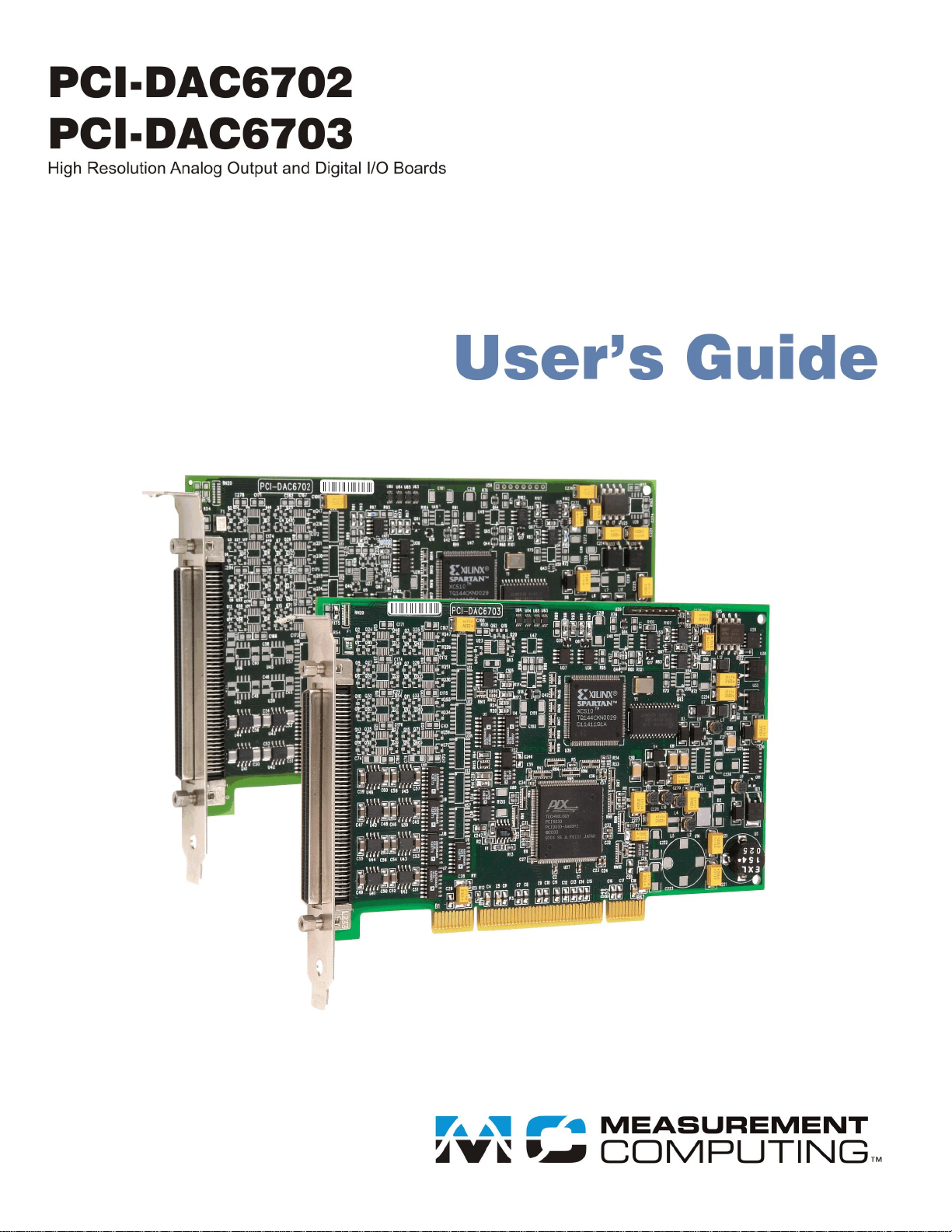
PCI-DAC6702 and
PCI-DAC6703
Analog Output and Digital I/O
User's Guide
Document Revision 3, March, 2009
© Copyright 2009, Measurement Computing Corporation
Page 3

HM PCI-DAC6702_03.doc
Your new Measurement Computing product comes with a fantastic extra —
Management committed to your satisfaction!
Thank you for choosing a Measurement Computing product—and congratulations! You own the finest, and you can now enjoy
the protection of the most comprehensive warranties and unmatched phone tech support. It’s the embodiment of our mission:
To provide PC-based data acquisition hardware and software that will save time and save money.
Simple installations minimize the time between setting up your system and actually making measurements. We offer quick and
simple access to outstanding live FREE technical support to help integrate MCC products into a DAQ system.
Limited Lifetime Warranty: Most MCC products are covered by a limited lifetime warranty against defects in materials or
workmanship for the life of the product, to the original purchaser, unless otherwise noted. Any products found to be defective in
material or workmanship will be repaired, replaced with same or similar device, or refunded at MCC’s discretion. For specific
information, please refer to the terms and conditions of sale.
Harsh Environment Program: Any Measurement Computing product that is damaged due to misuse, or any reason, may be
eligible for replacement with the same or similar device for 50% of the current list price. I/O boards face some harsh
environments, some harsher than the boards are designed to withstand. Contact MCC to determine your product’s eligibility for
this program.
30 Day Money-Back Guarantee: Any Measurement Computing Corporation product may be returned within 30 days of
purchase for a full refund of the price paid for the product being returned. If you are not satisfied, or chose the wrong product by
mistake, you do not have to keep it.
These warranties are in lieu of all other warranties, expressed or implied, including any implied warranty of merchantability or
fitness for a particular application. The remedies provided herein are the buyer’s sole and exclusive remedies. Neither
Measurement Computing Corporation, nor its employees shall be liable for any direct or indirect, special, incidental or
consequential damage arising from the use of its products, even if Measurement Computing Corporation has been notified in
advance of the possibility of such damages.
3
Page 4

Trademark and Copyright Information
TracerDAQ, Universal Library, Measurement Computing Corporation, and the Measurement Computing logo are either
trademarks or registered trademarks of Measurement Computing Corporation.
Windows, Microsoft, and Visual Studio are either trademarks or registered trademarks of Microsoft Corporation
LabVIEW is a trademark of National Instruments.
CompactFlash is a registered trademark of SanDisk Corporation.
XBee and XBee-PRO are trademarks of MaxStream, Inc.
All other trademarks are the property of their respective owners.
Information furnished by Measurement Computing Corporation is believed to be accurate and reliable. However, no
responsibility is assumed by Measurement Computing Corporation neither for its use; nor for any infringements of patents or
other rights of third parties, which may result from its use. No license is granted by implication or otherwise under any patent or
copyrights of Measurement Computing Corporation.
All rights reserved. No part of this publication may be reproduced, stored in a retrieval system, or transmitted, in any form by any
means, electronic, mechanical, by photocopying, recording, or otherwise without the prior written permission of Measurement
Computing Corporation.
Notice
Measurement Computing Corporation does not authorize any Measurement Computing Corporation product for use
in life support systems and/or devices without prior written consent from Measurement Computing Corporation.
Life support devices/systems are devices or systems which, a) are intended for surgical implantation into the body,
or b) support or sustain life and whose failure to perform can be reasonably expected to result in injury.
Measurement Computing Corporation products are not designed with the components required, and are not subject
to the testing required to ensure a level of reliability suitable for the treatment and diagnosis of people.
4
Page 5

Table of Contents
Preface
About this User's Guide ....................................................................................................................... 6
What you will learn from this user's guide ......................................................................................................... 6
Conventions in this user's guide ......................................................................................................................... 6
Where to find more information ......................................................................................................................... 6
Register-level programming ............................................................................................................................... 7
Chapter 1
Introducing the PCI-DAC6702 and PCI-DAC6703 .............................................................................. 8
Overview: PCI-DAC6702 and PCI-DAC6703 features ..................................................................................... 8
PCI-DAC6702 and PCI-DAC6703 block diagram ............................................................................................. 9
Software features ................................................................................................................................................ 9
Chapter 2
Installing the PCI-DAC6702 and PCI-DAC6703 ................................................................................ 10
What comes with your PCI-DAC6702 and PCI-DAC6703 shipment? ............................................................ 10
Hardware .........................................................................................................................................................................10
Additional documentation ................................................................................................................................................10
Optional components .......................................................................................................................................................10
Unpacking the PCI-DAC6702 and PCI-DAC6703 .......................................................................................... 11
Installing the software ...................................................................................................................................... 11
Installing the PCI-DAC6702 and PCI-DAC6703 ............................................................................................. 11
Connecting the board for I/O operations .......................................................................................................... 12
Connectors, cables – main I/O connector .........................................................................................................................12
Pinout – main I/O connector ............................................................................................................................................13
Cabling .............................................................................................................................................................................15
Field wiring and signal termination accessories ...............................................................................................................16
Chapter 3
Calibrating the PCI-DAC6702 and PCI-DAC6703 ............................................................................. 17
Calibration theory ............................................................................................................................................. 17
Chapter 4
Specifications ...................................................................................................................................... 18
Analog output ................................................................................................................................................... 18
Analog output calibration ................................................................................................................................. 19
Digital input / output ......................................................................................................................................... 19
Power consumption .......................................................................................................................................... 19
Environmental .................................................................................................................................................. 19
Mechanical ....................................................................................................................................................... 19
Main connector and pin out .............................................................................................................................. 20
Declaration of Conformity .................................................................................................................. 23
5
Page 6
Preface
About this User's Guide
What you will learn from this user's guide
This user's guide explains how to install, configure, and use the PCI-DAC6702 and PCI-DAC6703 boards so
that you get the most out of the voltage and current analog outputs and digital I/O features. This user’s guide
also refers you to related documents available on our web site, and to technical support resources.
Conventions in this user's guide
For more information on …
Text presented in a box signifies additional information and helpful hints related to the subject matter you are
reading.
Caution! Shaded caution statements present information to help you avoid injuring yourself and others,
damaging your hardware, or losing your data.
< : > Angle brackets that enclose numbers separated by a colon signify a range of numbers, such as those assigned
to registers, bit settings, etc.
bold text Bold text is used for the names of objects on the screen, such as buttons, text boxes, and check boxes. For
example:
1. Insert the disk or CD and click the OK button.
italic text Italic text is used for the names of manuals and help topic titles, and to emphasize a word or phrase. For
example:
The InstaCal installation procedure is explained in the Quick Start Guide.
Never touch the exposed pins or circuit connections on the board.
Where to find more information
The following electronic documents provide helpful information relevant to the operation of the PCI-DAC6702
and PCI-DAC6703 boards.
MCC's Specifications: PCI-DAC6702 and PCI-DAC6703 (the PDF version of the Specifications chapter in
this guide) is available on our web site at www.mccdaq.com/pdfs/Specs/PCI-DAC670x-spec.pdf.
MCC's Quick Start Guide is available on our web site at
www.mccdaq.com/PDFmanuals/DAQ-Software-Quick-Start.pdf.
MCC's Guide to Signal Connections is available on our web site at
www.mccdaq.com/signals/signals.pdf.
MCC's Universal Library User's Guide is available on our web site at
www.mccdaq.com/PDFmanuals/sm-ul-user-guide.pdf.
MCC's Universal Library Function Reference is available on our web site at
www.mccdaq.com/PDFmanuals/sm-ul-functions.pdf.
MCC's Universal Library for LabVIEW™ User’s Guide is available on our web site at
www.mccdaq.com/PDFmanuals/SM-UL-LabVIEW.pdf.
PCI-DAC6702 and PCI-DAC6703 User's Guide (this document) is also available on our web site at
www.mccdaq.com/PDFmanuals/PCI-DAC670x.pdf.
6
Page 7

PCI-DAC6702 and PCI-DAC6703 User's Guide About this User's Guide
Register-level programming
You should use the Universal Library to control your board. Only experienced programmers should try registerlevel programming.
If you need to program at the register level in your application, refer to the Register Map for the PCI-DAC6700
Series. This document is available on our website at www.mccdaq.com/registermaps/RegMapPCI-
DAC670x.pdf.
7
Page 8

Chapter 1
Introducing the PCI-DAC6702 and PCI-DAC6703
Overview: PCI-DAC6702 and PCI-DAC6703 features
This manual explains how to install and use your PCI-DAC6702 or PCI-DAC6703 board.
PCI-DAC6702 and PCI-DAC6703 boards are high-resolution analog output and digital I/O boards designed for
PCI bus-compatible computers. You can use PCI-DAC6702 and PCI-DAC6703 boards for various digital I/O
and DC setpoint applications.
The PCI-DAC6702 provides 8 analog outputs, and the PCI-DAC6703 provides 16 analog outputs. The voltage
output range for each board is ±10.1V volts.
Each board has eight TTL-compatible digital I/O channels that are configured as one eight-bit port. You can
configure each channel individually as either input or output. Digital channels are configured as inputs by
default. Digital bits are pulled up to +5V with 47k resistors. Positions are available for pull-down resistors.
PCI-DAC6702 and PCI-DAC6703 boards have a 16-bit digital to analog converter (DAC) that may be
periodically updated with new channel data. DAC channel data is stored in nonvolatile RAM (nvRAM). Each
channel has a main circuit that maintains the channel value between DAC updates.
PCI-DAC6702 and PCI-DAC6703 boards are equipped with an onboard temperature sensor that measures the
air temperature flowing over the board.
Each board features plug-and-play installation and on-board digital calibration. All I/O signals are transmitted
through a 100-pin connector.
8
Page 9

PCI-DAC6702 and PCI-DAC6703 User's Guide Introducing the PCI-DAC6702 and PCI-DAC6703
Bus Interface
Logic
+5V
100-Pin I/O Connector
0.75 A
Resettable
circuit breaker
Data
Address
Control
LOCAL BUS
Temperature
Sensor
Digital I/O
8-bit
Control
Voltage
Output
Circuit
Main
Voltage
Circuit
16-Bit
DAC
DIO (7:0)
RAM
Data
nvRAM
PCI BUS (5V, 32-Bit, 33MHZ)
RAM
Address/
Control
DAC
Out
PCI-DAC6703 x 16
PCI-DAC6702 x 8
PCI-DAC6702 and PCI-DAC6703 block diagram
PCI-DAC6702 and PCI-DAC6703 board functions are illustrated in the block diagram shown here.
Software features
Figure 1. PCI-DAC6702 and PCI-DAC6703 functional block diagram
For information on the features of InstaCal and the other software included with your PCI-DAC6702 and PCIDAC6703, refer to the Quick Start Guide that shipped with your device. The Quick Start Guide is also available
in PDF at www.mccdaq.com/PDFmanuals/DAQ-Software-Quick-Start.pdf.
Check www.mccdaq.com/download.htm for the latest software version or versions of the software supported
under less commonly used operating systems.
9
Page 10

PCI-DAC6702
PCI-DAC6703
C100HD50-x
C100MMS-x
Chapter 2
Installing the PCI-DAC6702 and PCI-DAC6703
What comes with your PCI-DAC6702 and PCI-DAC6703 shipment?
The following items are shipped with the PCI-DAC6702 and PCI-DAC6703.
Hardware
The following items should be included with your shipment.
PCI-DAC6702 or PCI-DAC6703
Additional documentation
In addition to this hardware user's guide, you should also receive the Quick Start Guide (available in PDF at
www.mccdaq.com/PDFmanuals/DAQ-Software-Quick-Start.pdf). This booklet supplies a brief description of
the software you received with your PCI-DAC6702 and PCI-DAC6703 and information regarding installation
of that software. Please read this booklet completely before installing any software or hardware.
Optional components
If you ordered any of the following products with your board, they should be included with your shipment.
Cables
10
Page 11

PCI-DAC6702 and PCI-DAC6703 User's Guide Installing the PCI-DAC6702 and PCI-DAC6703
Signal termination and conditioning accessories
MCC provides signal termination products for use with the PCI-DAC6702 and PCI-DAC6703. Refer to the
"Field wiring and signal termination accessories" section page 16 for a complete list of compatible accessory
products.
Unpacking the PCI-DAC6702 and PCI-DAC6703
As with any electronic device, you should take care while handling to avoid damage from static
electricity. Before removing the PCI-DAC6702 and PCI-DAC6703 from its packaging, ground yourself using a
wrist strap or by simply touching the computer chassis or other grounded object to eliminate any stored static
charge.
If any components are missing or damaged, notify Measurement Computing Corporation immediately by
phone, fax, or e-mail:
Phone: 508-946-5100 and follow the instructions for reaching Tech Support.
Fax: 508-946-9500 to the attention of Tech Support
Email: techsupport@mccdaq.com
Installing the software
Refer to the Quick Start Guide for instructions on installing the software on the Measurement Computing Data
Acquisition Software CD. This booklet is available in PDF at www.mccdaq.com/PDFmanuals/DAQ-Software-
Quick-Start.pdf.
Installing the PCI-DAC6702 and PCI-DAC6703
PCI-DAC6702 and PCI-DAC6703 boards are completely plug-and-play, with no switches or jumpers to set.
Configuration is controlled by your system's BIOS. To install your board, follow the steps below:
Install the MCC DAQ software before you install your board
The driver needed to run your board is installed with the MCC DAQ software. Therefore, you need to install the
MCC DAQ software before you install your board. Refer to the Quick Start Guide for instructions on installing
the software.
1. Turn your computer off, open it up, and insert your board into an available PCI slot.
2. Close your computer and turn it on.
If you are using an operating system with support for plug-and-play (such as Windows 2000 or
Windows XP), a dialog box pops up as the system loads indicating that new hardware has been detected. If
the information file for this board is not already loaded onto your PC, you will be prompted for the disk
containing this file. The MCC DAQ software contains this file. If required, insert the Measurement
Computing Data Acquisition Software CD and click OK.
3. To test your installation and configure your board, run the InstaCal utility installed in the previous section.
Refer to the Quick Start Guide that came with your board for information on how to initially set up and
load InstaCal.
If your board has been powered-off for more than 10 minutes, allow your computer to warm up for at least
15 minutes before acquiring data. This warm-up period is required in order for the board to achieve its rated
accuracy. The high speed components used on the board generate heat, and it takes this amount of time for a
board to reach steady state if it has been powered off for a significant amount of time.
11
Page 12

PCI-DAC6702 and PCI-DAC6703 User's Guide Installing the PCI-DAC6702 and PCI-DAC6703
Connector type
Shielded, SCSI 100-pin D-type
Compatible cables
C100HD50-x unshielded round cable. x = 3 or 6 feet. (Figure )
C100MMS-x shielded round cable. x = 1, 2, or 3 meters. (Error! Reference
source not found.)
Compatible accessory products with the
C100HD50-x cable
BNC-16SE
BNC-16DI
CIO-MINI50
CIO-TERM100
SCB-50
Compatible accessory products with the
C100MMS-x cable
SCB-100
BNC-DI-FE
Connecting the board for I/O operations
Connectors, cables – main I/O connector
The table below lists the board connectors, applicable cables, and compatible accessory products for the PCIDAC6702 and PCI-DAC6703.
Board connectors, cables, and accessory equipment
Information on signal connections
General information regarding signal connection and configuration is available in the Guide to Signal
Connections. This document is available on our web site at
www.measurementcomputing.com/signals/signals.pdf.
12
Page 13

PCI-DAC6702 and PCI-DAC6703 User's Guide Installing the PCI-DAC6702 and PCI-DAC6703
Signal name
Pin Pin
Signal name
GND
100
50
GND
n/c
99
49
n/c
n/c
98
48
DIO7
n/c
97
47
DIO6
GND
96
46
DIO5
n/c
95
45
DIO4
n/c
94
44
n/c
n/c
93
43
DIO3
DIO7
92
42
DIO2
DIO6
91
41
DIO1
DIO5
90
40
DIO0
DIO4
89
39
PC 5V
DIO3
88
38
n/c
DIO2
87
37
n/c
DIO1
86
36
n/c
DIO0
85
35
n/c
AGND
84
34
AGND15
n/c
83
33
VCH15
AGND
82
32
AGND14
n/c
81
31
VCH14
AGND
80
30
AGND13
n/c
79
29
VCH13
AGND
78
28
AGND12
n/c
77
27
VCH12
AGND
76
26
AGND11
n/c
75
25
VCH11
AGND
74
24
AGND10
n/c
73
23
VCH10
AGND
72
22
AGND9
n/c
71
21
VCH9
AGND
70
20
AGND8
n/c
69
19
VCH8
AGND
68
18
AGND
AGND
67
17
AGND7
n/c
66
16
VCH7
AGND
65
15
AGND6
n/c
64
14
VCH6
AGND
63
13
AGND5
n/c
62
12
VCH5
AGND
61
11
AGND4
n/c
60
10
VCH4
AGND
59 9 AGND3
n/c
58 8 VCH3
AGND
57 7 AGND2
n/c
56 6 VCH2
AGND
55 5 AGND1
n/c
54 4 VCH1
AGND
53 3 AGND0
n/c
52 2 VCH0
AGND
51 1 AGND
PCI slot ↓
Pinout – main I/O connector
The main I/O connector pinouts for each board are shown in the following tables. Note that the DIO[7:0]
signals are provided in two locations in order to provide flexibility for applications which use the C100HD50-x
ribbon cable.
PCI-DAC6703 connector pin out
13
Page 14

PCI-DAC6702 and PCI-DAC6703 User's Guide Installing the PCI-DAC6702 and PCI-DAC6703
Signal name
Pin
Pin
Signal name
GND
100
50
GND
n/c
99
49
n/c
n/c
98
48
DIO7
n/c
97
47
DIO6
GND
96
46
DIO5
n/c
95
45
DIO4
n/c
94
44
n/c
n/c
93
43
DIO3
DIO7
92
42
DIO2
DIO6
91
41
DIO1
DIO5
90
40
DIO0
DIO4
89
39
PC 5V
DIO3
88
38
n/c
DIO2
87
37
n/c
DIO1
86
36
n/c
DIO0
85
35
n/c
AGND
84
34
AGND
n/c
83
33
n/c
AGND
82
32
AGND
n/c
81
31
n/c
AGND
80
30
AGND
n/c
79
29
n/c
AGND
78
28
AGND
n/c
77
27
n/c
AGND
76
26
AGND
n/c
75
25
n/c
AGND
74
24
AGND
n/c
73
23
n/c
AGND
72
22
AGND
n/c
71
21
n/c
AGND
70
20
AGND
n/c
69
19
n/c
AGND
68
18
AGND
AGND
67
17
AGND7
n/c
66
16
VCH7
AGND
65
15
AGND6
n/c
64
14
VCH6
AGND
63
13
AGND5
n/c
62
12
VCH5
AGND
61
11
AGND4
n/c
60
10
VCH4
AGND
59
9
AGND3
n/c
58
8
VCH3
AGND
57
7
AGND2
n/c
56
6
VCH2
AGND
55
5
AGND1
n/c
54
4
VCH1
AGND
53
3
AGND0
n/c
52
2
VCH0
AGND
51
1
AGND
PCI slot ↓
PCI-DAC6702 connector pin out
14
Page 15

PCI-DAC6702 and PCI-DAC6703 User's Guide Installing the PCI-DAC6702 and PCI-DAC6703
1
50
2
49
51
100
52
99
10050
511
Strain relief is
stamped “Pins 1-50”.
Pins 1-50 are on the long side
of the “D” connector.
Pins 51-100 are on
the short side of
the “D” connector.
Key
Key
The red stripe
identifies pin # 1
The red stripe
identifies pin # 51
Strain relief is
Stamped “Pins 51-100”.
10050
511
10050
511
Cabling
Details on the cables below are available on our web site at www.mccdaq.com/products/accessories.aspx.
Figure 2. C100HD50-x cable
Figure 3. C100MMS-x cable
15
Page 16

PCI-DAC6702 and PCI-DAC6703 User's Guide Installing the PCI-DAC6702 and PCI-DAC6703
Field wiring and signal termination accessories
You can use the following BNC and screw terminal boards to terminate field signals and route them into the
PCI-DAC6702 and PCI-DAC6703 boards using the C100HD50-x cable:
BNC-16SE – Brings analog signals to standard BNC connectors. Designed for boards operating in single-
ended mode.
BNC-16DI – Brings analog signals to standard BNC connectors. Designed for boards operating in
differential mode.
CIO-MINI50 – 50-pin screw terminal board. Two boards are required.
CIO-TERM100 – 100-pin screw terminal board (daisy-chained 50-pin IDC connectors).
SCB-50 – 50 conductor, shielded signal connection/screw terminal box provides two independent 50-pin
connections.
You can use the following screw terminal box and BNC connector box to terminate field signals and route them
into the PCI-DAC6702 and PCI-DAC6703 board using the C100MMS-x cable:
SCB-100 – 100 conductor, shielded signal connection/screw terminal box provides two independent 50-pin
connections.
BNC-16DI-FE – Brings analog signals to standard BNC connectors. Designed to be compatible with the
100-pin shielded C100MMS-x cable.
Details on these products are available on our web site at www.mccdaq.com/products/screw_terminal_bnc.aspx.
16
Page 17

Trim DAC
Ref
D/A
Gain
Adjust
Analog Out
Trim DAC
Offset
Adjust
Chapter 3
Calibrating the PCI-DAC6702 and PCI-DAC6703
You should calibrate the board using the InstaCal utility software after the board has fully warmed up. The
recommended warm-up time is 15 minutes. For best results, calibrate the board immediately before use. The
high resolution analog components on the board are temperature-sensitive, so calibrating the board before use
ensures that your board is operating with the optimum calibration values. All calibration values are saved in
nvRAM.
Calibration theory
InstaCal calibrates the board's analog outputs for offset and gain (see Figure 4). A trim DAC is used to adjust
the gain of the DAC. A separate DAC is used to adjust offset on the final output amplifier.
Figure 4. Analog output calibration
Calibration schedule
You should calibrate your PCI-DAC6702 and PCI-DAC6703 board once per year using InstaCal's calibration
procedures.
17
Page 18

D/A converter type
Enhanced R-2R
Resolution
16-bits, 1 in 65536
Number of channels
PCI-DAC6703: 16 voltage
PCI-DAC6702: 8 voltage
DNL
±1 LSB max
Monotonicity
16-bits, guaranteed after calibration
Update rate, max
PCI-DAC6703: 1111 S/s per channel
PCI-DAC6702: 1111 S/s per channel
Update modes
Software selectable per channel for update immediate (default), or update from
NVRAM on command
Output short-circuit duration
Indefinite @ 25 mA
Power-on state
Independent, user-defined power-on states.
Range
±10.1 V
Output coupling
DC
Output impedance
0.1 Ω max.
Current drive
±10 mA max
Load capacitance
10,000 pF
Slew rate
0.5 V/µs typ.
Settling time (full scale step)
7.2 ms max to ±0.5 LSB
Noise
100 µVrms, DC to 1 MHz BW
Offset temperature coefficient
±5 µV/ºC
Gain temperature coefficient
±1 ppm/ºC
Protection
Short circuit to ground
Data transfer
Programmed I/O
Range1
% of Reading
Offset
Temp Drift
2
(%/ºC)
Absolute Accuracy at FS
±10 V
0.0019
±710 µV
0.0001
±1 mV
Range
Relative Accuracy
±10 V
±1.0 LSB, max
Specifications
Typical for 25 °C unless otherwise specified.
Specifications in italic text are guaranteed by design
Analog output
Table 1. Analog output specifications
Chapter 4
Table 2. Voltage output specifications
Table 3. Absolute accuracy components - all values are (±)
Note 1: Temp drift applies only if the ambient temperature changes by more than ±10ºC since the last
calibration.
Note 2: Each PCI-DAC670x board is tested at the factory to assure that the overall error does not exceed
the values specified in Table 3.
Table 4. Relative accuracy
Relative accuracy is defined as the measured deviation from a straight line drawn between measured endpoints
of the transfer function.
18
Page 19

PCI-DAC6702 and PCI-DAC6703 User's Guide Specifications
Recommended warm-up time
15 minutes
Calibration
Auto-calibration, calibration factors for each range stored on board in non-volatile
RAM.
Onboard calibration reference
DC Level: 10.000 V± 1 mV. Actual measured values stored in EEPROM.
Tempco: 0.6 ppm/°C max
Long-term stability: ±6 ppm/sqrt(1000 hrs)
Calibration interval
1 year
Digital type
Discrete, 5 V/TTL compatible
Number of I/O
8
Configuration
8 bits, independently programmable for input or output. Position available for
pull-up/pull-down resistor network (not populated).
Input high voltage
2.0 V min, 7.0 V absolute max
Input low voltage
0.8 V max, –0.5 V absolute min
Output high voltage
(IOH = –32 mA)
3.80 V min, 4.20 V typ
Output low voltage
(IOL = 32 mA)
0.55 V max, 0.22 V typ
Data transfer
Programmed I/O
Power-up / reset state
Input mode (high impedance)
+5 V
PCI-DAC6703: 1.1 A max
PCI-DAC6702: 1.0 A max
+5 V available at I/O connector
0.75A max, protected with a resettable fuse
Operating temperature range
0 to 55 °C
Storage temperature range
-20 to 70 °C
Humidity
0 to 90% non-condensing
Card dimensions
PCI half card: 174.4 mm (L) x 106.9 mm (W) x18.4 mm (H)
Form factor
Universal PCI keying. Compatible with either 3.3 V or 5 V PCI signaling
environments.
Analog output calibration
Table 5. Analog I/O calibration
Digital input / output
Table 6. Digital I/O
Power consumption
Environmental
Mechanical
Table 7. Power consumption specifications
Table 8. Environmental specifications
Table 9. Mechanical specifications
19
Page 20

PCI-DAC6702 and PCI-DAC6703 User's Guide Specifications
Connector type
Shielded SCSI 100 D-Type
Compatible cables
C100HD50-x, unshielded ribbon cable.
x = 3 or 6 feet
C100MMS-x, shielded round cable.
x = 1, 2, or 3 meters
Compatible accessory products
(with C100HD50-x cable)
BNC-16SE
BNC-16DI
CIO-MINI50
CIO-TERM100
SCB-50
Compatible accessory products
(with C100MMS-x cable)
SCB-100
BNC-16DI-FE
Main connector and pin out
Table 10. Main connector specifications
20
Page 21

PCI-DAC6702 and PCI-DAC6703 User's Guide Specifications
Pin
Signal Name
Pin
Signal Name
1
AGND
51
AGND
2
VCH0
52
n/c 3 AGND0
53
AGND
4
VCH1
54
n/c
5
AGND1
55
AGND
6
VCH2
56
n/c
7
AGND2
57
AGND
8
VCH3
58
n/c 9 AGND3
59
AGND
10
VCH4
60
n/c
11
AGND4
61
AGND
12
VCH5
62
n/c
13
AGND5
63
AGND
14
VCH6
64
n/c
15
AGND6
65
AGND
16
VCH7
66
n/c
17
AGND7
67
AGND
18
AGND
68
AGND
19
VCH8
69
n/c
20
AGND8
70
AGND
21
VCH9
71
n/c
22
AGND9
72
AGND
23
VCH10
73
n/c
24
AGND10
74
AGND
25
VCH11
75
n/c
26
AGND11
76
AGND
27
VCH12
77
n/c
28
AGND12
78
AGND
29
VCH13
79
n/c
30
AGND13
80
AGND
31
VCH14
81
n/c
32
AGND14
82
AGND
33
VCH15
83
n/c
34
AGND15
84
AGND
35
n/c
85
DIO0
36
n/c
86
DIO1
37
n/c
87
DIO2
38
n/c
88
DIO3
39
PC 5V
89
DIO4
40
DIO0
90
DIO5
41
DIO1
91
DIO6
42
DIO2
92
DIO7
43
DIO3
93
n/c
44
n/c
94
n/c
45
DIO4
95
n/c
46
DIO5
96
GND
47
DIO6
97
n/c
48
DIO7
98
n/c
49
n/c
99
n/c
50
GND
100
GND
Table 11. PCI-DAC6703 pin out
Note 3: Note: DIO[7:0] signals are provided in two locations in order to provide flexibility for
applications which use the C100HD50-x ribbon cable.
21
Page 22

PCI-DAC6702 and PCI-DAC6703 User's Guide Specifications
Pin
Signal Name
Pin
Signal Name
1
AGND
51
AGND
2
VCH0
52
n/c 3 AGND0
53
AGND
4
VCH1
54
n/c
5
AGND1
55
AGND
6
VCH2
56
n/c
7
AGND2
57
AGND
8
VCH3
58
n/c 9 AGND3
59
AGND
10
VCH4
60
n/c
11
AGND4
61
AGND
12
VCH5
62
n/c
13
AGND5
63
AGND
14
VCH6
64
n/c
15
AGND6
65
AGND
16
VCH7
66
n/c
17
AGND7
67
AGND
18
AGND
68
AGND
19
n/c
69
n/c
20
AGND
70
AGND
21
n/c
71
n/c
22
AGND
72
AGND
23
n/c
73
n/c
24
AGND
74
AGND
25
n/c
75
n/c
26
AGND
76
AGND
27
n/c
77
n/c
28
AGND
78
AGND
29
n/c
79
n/c
30
AGND
80
AGND
31
n/c
81
n/c
32
AGND
82
AGND
33
n/c
83
n/c
34
AGND
84
AGND
35
n/c
85
DIO0
36
n/c
86
DIO1
37
n/c
87
DIO2
38
n/c
88
DIO3
39
PC 5V
89
DIO4
40
DIO0
90
DIO5
41
DIO1
91
DIO6
42
DIO2
92
DIO7
43
DIO3
93
n/c
44
n/c
94
n/c
45
DIO4
95
n/c
46
DIO5
96
GND
47
DIO6
97
n/c
48
DIO7
98
n/c
49
n/c
99
n/c
50
GND
100
GND
Table 12. PCI-DAC6702 pin out
Note 4: DIO[7:0] signals are provided in two locations in order to provide flexibility for applications
which use the C100HD50-x ribbon cable.
22
Page 23

Declaration of Conformity
Manufacturer: Measurement Computing Corporation
Address: 10 Commerce Way
Suite 1008
Norton, MA 02766
USA
Category: Electrical equipment for measurement, control and laboratory use.
Measurement Computing Corporation declares under sole responsibility that the product
PCI-DAC6702 and PCI-DAC6703
to which this declaration relates is in conformity with the relevant provisions of the following standards or other
documents:
EC EMC Directive 2004/108/EC: Electromagnetic Compatibility, EN 61326-1:2006 (IEC 61326-1:2005)
Emissions: Group 1, Class B
EN 55011(1990)/CISPR 11: Radiated and Conducted emissions.
Immunity: EN61326-1:2006, (IEC 61326-1:2005)
EN61000-4-2 (2001): Electrostatic Discharge immunity.
EN61000-4-3 (2002): Radiated Electromagnetic Field immunity.
EN61000-4-4 (2004): Electric Fast Transient Burst immunity.
EN61000-4-5 (2001): Surge immunity.
EN61000-4-6 (2003): Radio Frequency Common Mode immunity.
EN61000-4-11 (2004): Voltage Dip and Interrupt immunity.
Declaration of Conformity based on tests conducted by Chomerics Test Services, Woburn, MA 01801, USA in
May, 2004. Test records are outlined in Chomerics Test Report #EMI3887.04. Further testing was conducted by
Chomerics Test Services, Woburn, MA. 01801, USA in December, 2008. Test records are outlined in
Chomerics Test report #EMI5241.08.
We hereby declare that the equipment specified conforms to the above Directives and Standards.
Carl Haapaoja, Director of Quality Assurance
Page 24

Measurement Computing Corporation
10 Commerce Way
Suite 1008
Norton, Massachusetts 02766
(508) 946-5100
Fax: (508) 946-9500
E-mail: info@mccdaq.com
www.mccdaq.com
 Loading...