

Page 1

PC104-PDISO8
User’s Manual
Revision 3
October, 2000
Page 2

Your new Measurement Computing product comes with a fantastic extra —
Management committed to your satisfaction!
Thank you for choosing a Measurement Computing product—and congratulations! You own the finest, and you can now enjoy
the protection of the most comprehensive warranties and unmatched phone tech support. It’s the embodiment of our mission:
To provide data acquisition hard ware and software that will save time and save money.
Simple installations minimize the time between setting up your system and actually making measurements. We offer quick and
simple access to outstanding live FREE technical support to help integrate MCC products into a DAQ system.
Limited Lifetime Warranty: Most MCC products are covered by a limited lifetime warranty against defects in materials or
workmanship for the life of the product, to the original purchaser, unless otherwise noted. Any products found to be defective in
material or workmanship will be repaired, replaced with s ame or s imilar device, or refunded at MCC’s discretion. For specific
information, please refer to the terms and conditions of sale.
Harsh Environment Program: Any Measurement Computing product that is damaged due to misuse, or any reason, may be
eligible for replacement with the same or similar device for 5 0% of the current list price. I/O boards face some harsh
environments, some harsher than the boards are designed to withstand. Contact MCC to determine your product’s eligibility for
this program.
30 Day Money-Back Guarantee: Any Measurement Computing Corporation product may be returned within 30 days of
purchase for a full refund of the price paid for the product being returned. If you are not satisfied, or chose the wrong product by
mistake, you do not have to keep it.
These warranties are in lieu of all other warranties, expressed or implied, including any implied warranty of merchantability or
fitness for a particular application. The remedies provided herein are the buyer’s sole and exclusive remedies. Neither
Measurement Computing Corporation, nor its employees shall be liable for any direct or indirect, special, incidental or
consequential damage arising from the use of its products, even if Measurement Computing Corporation has been notified in
advance of the possibility of such damages.
Trademark and Copyright Inf ormatio n
Measurement Computing Corporation, InstaCal, Universal Library, and the Measurement Computing logo are eit her trademarks
or registered trademarks of Measurement Computing Corporation. Refer to the Copyrights & Trademarks section on
mccdaq.com/legal
mentioned herein are tr ademarks or trade names of their respect ive companies.
© 2000 Measurement Computing Corporation. All rights reserved. No part of this publication may be reproduced, stored in a
retrieval system, or transmitted, in any form by any means, electronic, mechanical, by photocopying, recording, or otherwise
without the prior written permission of Measurement Computing Corporation.
Notice
Measurement Computing Corporation does not authorize any Measurement Computing Corporation product for use
in life support systems and/or devices without prior written consent from Measure ment Computing Corporation.
Life support devices/systems are devices or systems that, a) are intended for surgical implantation into the body, or
b) support or sustain life and whose failure to perform can be reasonably expected to result in injury. Measurement
Computing Corporation products are not designed with the components required, and are not subject to the testing
required to ensure a level of reliability suitable for the treatment and diagnosis of people.
HM PC104-PDISO8.lwp
for more information about Measurement Computing trademarks. Other product and company names
Page 3

1 INTRODUCTION ....................................
2 INSTALLATION .....................................
3 REGISTER DESCRIPTIONS ...........................
4 ELECTRONICS AND INTERFACING ..................
5 SPECIFICATIONS ..................................
1
11.1 DESCRIPTION ...................................
11.2 ACCESSORIES ...................................
2
22.1 SOFTWARE ......................................
22.2 BASE ADDRESS ..................................
32.3 AC INPUT FILTER ................................
5
53.1 INTRODUCTION .................................
63.2 OUTPUT REGISTER ...............................
73.3 INPUT REGISTER .................................
8
84.1 I/O CONNECTOR ................................
94.1 FORM C RELAY OUTPUTS .........................
94.2 FORM A RELAY OUTPUTS .........................
104.3 ISOLATED INPUTS ..............................
104.4 EXTENDING THE INPUT RANGE ...................
11
Page 4

This page was intentionally left blank.
Page 5

1 INTRODUCTION
1.1 DESCRIPTION
The PC104-PDISO8 has 8-channels of isolated inputs and relay outputs. The board is
designed for sensing and control applications having high voltages.
WARNING!
High voltages will be present on the board when you have
connected high voltage inputs or outputs to the connector.
Use extreme caution! Never handle the board when live signals are
connected to the board via the connector.
The eight outputs are electromechanical relays. Five provide FORM C connections
and three provide normally-open FORM A connection. The relays are controlled by
writing to one 8-bit port. The state of the relay control register may be read back.
The inputs are eight individual, optically-isolated inputs that may be read back as a
single byte. The inputs are not polarity sensitive and may be driven by either AC
(input range −24V to +24V RMS, 50 to 1000 Hz) or DC (input range −24V to
+24VDC). Each input has a switchable low-pass filter.
Although requiring only two, 8-bit ports, the board occupies four ports.
1.2 ACCESSORIES
The PC104-PDISO8 is a combination digital I/O board with signal conditioning
installed. Most accessory boards are intended to provide signal conditioning or easy
to access signal termination. In general, it does not require additional signal
conditioning.
WARNING
We strongly recommend
PC104-PDISO8. The board is intended to sense and control high voltages. A screw
terminal board would expose yourself and others to high voltage signals.
Rather, we recommend that you construct a safe cable to carry your signals directly
from your equipment to the board’s connector.
against
using screw terminal boards with the
1
Page 6
2.1 SOFTWARE
2 INSTALLATION
Before you open your computer and install the board, install and run
installation, calibration and test utility included with your board.
you through switch and jumper settings for your board. Detailed information
regarding these settings can be found below. Refer to the
Installation Manual
for
Insta
Cal installation instructions.
Insta
Cal, the
Insta
Cal will guide
Extended Software
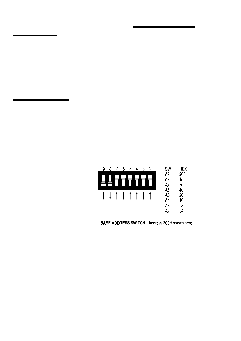
2.2 BASE ADDRESS
The base address switch controls the I/O location where the CPU can access the
board’s registers.
The factory default is 300 hex (768 decimal).
If you already have a board installed at address 300h, choose a new address from
those available on your computer.
Use the list of PC I/O address
assignments found in Table 2-1 to
determine the appropriate address.
Choose a new base address from
those available and set the switch
using the guide to the right.
If 300 hex is available on your
computer, there is no need to
change this switch from the factory
default setting.
Figure 2-1. Base Address Switch
2
Page 7

Table 1-1. PC I/O Addresses
FUNCTIONHEX
RANGE
070-071
The BASE switches can be set for an address in the range of 000-3F8 so it should not
be hard to find a free address. Addresses not specifically listed, such as 390-39F, are
free.
CMOS RAM & NMI MASK (AT)
RANGE
FUNCTIONHEX
EGA2C0-2CF8237 DMA #1000-00F
EGA2D0-2DF8259 PIC #1020-021
GPIB (AT)2E0-2E78253 TIMER040-043
SERIAL PORT2E8-2EF8255 PPI (XT)060-063
SERIAL PORT2F8-2FF8742 CONTROLLER (AT)060-064
PROTOTYPE CARD300-30F
PROTOTYPE CARD310-31FDMA PAGE REGISTERS080-08F
HARD DISK (XT)320-32F8259 PIC #2 (AT)0A0-0A1
PARALLEL PRINTER378-37FNMI MASK (XT)0A0-0AF
SDLC380-38F8237 #2 (AT)0C0-0DF
SDLC3A0-3AF80287 NUMERIC CO-P (AT)0F0-0FF
MDA3B0-3BBHARD DISK (AT)1F0-1FF
PARALLEL PRINTER3BC-3BFGAME CONTROL200-20F
EGA3C0-3CFEXPANSION UNIT (XT)210-21F
CGA3D0-3DFBUS MOUSE238-23B
SERIAL PORT3E8-3EFALT BUS MOUSE23C-23F
FLOPPY DISK3F0-3F7PARALLEL PRINTER270-27F
SERIAL PORT3F8-3FFEGA2B0-2BF
2.3 AC INPUT FILTER
The inputs are eight individual, optically isolated (500V) inputs that may be read back
as a single byte. The inputs are not po larity sensitive and can be driven by either AC
(input range −24V to +24V RMS, 50 to 1000 Hz) or DC (input range −24V to
+24VDC). Each input has a switchable low-pass filter.
The switch which controls the input
filter is shown in Figure 2-2. From left
to right, the switches apply to inputs 0
to 7. The diagram shows the low pass
filter for inputs 0 and 1 enabled.
The filter must be used for AC inputs
and should be used for DC inputs.
Unless you have reason to turn off a
filter, we recommend it be left on. Figure 2-2. AC Filter Switches
3
Page 8

WARNING
High voltages will be present on the board when you have
connected high voltage inputs or outputs to the connector.
Use extreme caution! Never handle the board when high voltage
signals are connected to the board.
4
Page 9

3 REGISTER DESCRIPTIONS
3.1 INTRODUCTION
Two, eight-bit registers located at the base address (relay output) and base + 1
(isolated inputs) are read or written to for control of relays, read back the state of
relays or sense inputs (Table 3-1).
Table 3-1. Board Registers
READ/WRITERELAY OUTPUTBASE ADDRESS
Relay OutputsBASE + 0
Read OnlyIsolated InputsBASE + 1
Not UsedBASE + 2
Not UsedBASE + 3
Although the PC104-PDISO8 decodes up to four addresses, two of those are not used.
This conforms to the design of the original PDISO-8, of which the PC104-PDISO8 is
a true clone.
Please use the Universal Library if you are programming from a high level language.
The registers are written to and read from as a single 8-bit byte. Each bit controls an
output or represents the state of an input.
Both registers are read left to right. The leftmost bit being the most significant bit.
Following this format, bit 7 of BASE + 0 corresponds to relay 7 and bit 0 to relay 0.
To construct a control word, refer to Table 3-2 for bit weights.
Table 3-2. Bit Weights
HEX VALUEDECIMAL VALUEBIT POSITION
110
221
442
883
10164
20325
40646
801287
Example: To assemble a control byte with relays 0, 1, 3, 5, and 7 turned ON , refer to
Table 3-3 for the coding.
5
Page 10

Table 3-3. Control Byte Example
ON=1DECIMALWEIGHTON=1HEXRELAY
If the relay status byte is read back, it is in the same format.
The isolated inputs are read in this format as well. To disassemble the byte and
determine the state of the isolated inputs or the relay read back register, perform the
following operation in software:
Table 3-4. Register Read-Back
HEXINPUT/RELAY
DECIMAL
WEIGHT
1281128801807
006400406
32132201205
001600104
8188183
0040042
2122121
1111110
171AB
12880INPUT 7/RELAY 7
6440INPUT 6/RELAY 6
3220INPUT 5/RELAY 5
1610INPUT 4/RELAY 4
88INPUT 3/RELAY 3
44INPUT 2/RELAY 2
22INPUT 1/RELAY 1
11INPUT 0/RELAY 0
3.2 OUTPUT REGISTER
The output register is located at the base address (BASE + 0).
WRITE = CONTROL: Write a byte to the register to control the relays. A one in the
relay bit position turns the relay.
READ = STATUS: Read the status of the relay control register. A one in the relay
bit position indicates the relay is on.
6
Page 11

3.2.1 ON & OFF for FORM C RELAYS
y
On means that FORM C relay common is in contact with the Normally-Open
(NO) contact.
y
Off means that FORM C relay common is in contact with the
Normally-Closed (NC) contact.
3.2.2 ON & OFF FOR FORM A RELAYS
y
On means that FORM A relay common is in contact with the Normally-Open
(NO) contact.
y
Off means that FORM A relay common is open.
3.3 INPUT REGISTER
The isolated input register is located at
WRITE = NO FUNCTION
READ = STATUS: Read the status of the isolated inputs. A one in the input bit
position indicates that a voltage is present at the input.
INPUT #
BIT No. 76543210
HEX 804020108421
DECIMAL 1286432168421
7 6 5 4 3 2 1 0
BASE
address + 1.
7
Page 12

4 ELECTRONICS AND INTERFACING
This short introduction to the electronics most o ften needed by digital I/O b oard users
covers the following:
y
Connector diagram.
y
FORM C relay outputs.
y
FORM A relay outputs.
y
Isolated inputs.
y
Adding a resistor to expand the range of the isolated inputs.
4.1 I/O CONNECTOR
The PC104-PDISO8 use a single 40-pin connector. The pin-outs of the connector are
shown in Figure 4-1. This connector can be converted to a 37 pin connector that is
compatible with the CIO-PDISO8 through the use o f an adapter such as the BP 40-37
(Figure 4-2).
Figure 4-1. I/O Connector Pin Out
WARNING
High voltages will be present on the board when connected to high
voltage inputs or outputs. Use extreme caution! Never handle the
board when live signals are connected to the board.
8
Page 13

Figure 4-2. BP40-37 Pinouts
4.1 FORM C RELAY OUTPUTS
Figure 4-3 is the schematic for a
form C relay, used at OP0 through
OP4.
The form C relay has a COMMON,
normally open (NO) and normally
closed (NC) contact.
When a 0 is written to the output,
the common and NC are in contact.
When a 1 is written to the output,
the common and NO are in contact.
Figure 4-3. Form C Relay
The pin numbers shown in Figure 4-2 correspond to the 37 pin connector when using
an adapter such as the BP40-37 or the C40-37F-2 cable for relay #0.
9
Page 14

4.2 FORM A RELAY OUTPUTS
Shown here is the schematic for a form A
relay, used at OP5 through OP7.
The form A relay has a COMMON and a
normally open (NO) contact.
When a 0 is written to the output, the
common and NO are NOT in contact. When
a 1 is written to the output the common and
NO are in contact. Figure 4-4 Form A Relay
The form A and form C relays are actually the same part number. Only the
connections to the relay poles differ.
The Pin numbers shown in Figure 4-4 correspond to the 37 pin connector when using
an adapter such as the BP40-37 or the C40-37F-2 cable for relay #5
.
4.3 ISOLATED INPUTS
There are eight optically-isolated input channels. The schematic of a single channel is
shown in Figure 4-4.
Optical
Isolator
455 Ohm
Figure 4-4. Input Circuit - Simplified
Input signals are fed to a bridge rectifier so that the inputs are not polarity-sensitive.
10
Page 15

4.4 EXTENDING THE INPUT RANGE
You can extend the input range beyond the ±24V specified by adding an external
resistor to the input. Use the following formulas:
R
= 100 * (Vin - 24)
ext
= R
Resistor power rating = P
watts
/ 10,000
ext
11
Page 16

5 SPECIFICATIONS
POWER CONSUMPTION
+5V supply 0.11 A typical with all relays off.
0.4 A typical with all relays on.
OUTPUT RELAY SPECIFICATIONS
Number 8
Contact arrangement 5 form C, Relay 0 to Relay 4
3 form A, Relay 5 to Relay 7
Contact rating (resistive load) 0.4 A @ 120VAC or 2 A @ 30VDC
Contact resistance 0.050 Ohms max.
Coil resistance 125 Ohms
Operate time 5 ms
Release time 5 ms max.
Isolation
Between open contacts 1000VAC, 50/60HZ, 1 min.
Between coil and contacts 1500VAC, 50/60HZ, 1 min.
Life Expectancy
Mechanical 100,000,000 Operations
Electrical 500,000 Operations @ Full Load
ISOLATED INPUTS
Number 8
Type Non-polarized, optically isolated (NOT TTL
compatible)
Range
DC ±24V
AC (50 to 1 kHz) ±24V
Input ‘High’ level >5V min. (positive or negative input voltage)
Input ‘Low’ level <2.5V max. (positive or negative input
voltage)
Isolation 500V
Resistance 455 Ohms min
Response 20 µs w/o filter
5 ms w/ filter
Filters
Time constant 5 ms (200 Hz)
Filter control Each input individually switch-selectable
12
Page 17

CONNECTOR
Connector type 40 pin male header (optional cable available
to translate 40 pin connector to 37 pin
connector compatible with CIO-PDISO8)
Dielectric Strength 1000Vrms
Current Rating 1 A
ENVIRONMENTAL
Operating temperature 0 to 50 deg. C
Storage temperature −20 to 70 deg. C
Humidity 0 to 90% non-condensing
13
Page 18

For your notes.
14
Page 19

EC Declaration of Conformity
Measurement Computing Corporation
We,
product:
PC104-PDISO8
DescriptionPart Number
to which this declaration relates, meets the essential requirements, is in conformity
with, and CE marking has been applied according to the relevant EC Directives listed
below using the relevant section of the following EC standards and other normative
documents:
, declare under sole responsibility that the
EU EMC Directive 89/336/EEC
compatibility.
EU 55022 Class B
characteristics of information technology equipment.
EN 50082-1
IEC 801-2
and control equipment.
IEC 801-3
measurements and control equipment.
IEC 801-4
equipment.
Carl Haapaoja, Director of Quality Assurance
: Electrostatic discharge requirements for industrial process measurement
: Radiated electromagnetic field requirements for industrial process
: Electrically fast transients for industrial process measurement and control
: Limits and methods of measurements of radio interference
: EC generic immunity requirements.
: Essential requirements relating to electromagnetic
Page 20

Measurement Computing Corporation
10 Commerce Way
Suite 1008
Norton, Massachusetts 02766
(508) 946-5100
Fax: (508) 946-9500
E-mail: info@mccdaq.com
www.mccdaq.com
 Loading...