

Page 1

PC104-DIO48
User’s Manual
Revision 4
April, 2001
Page 2

Your new Measurement Computing product comes with a fantastic extra —
Management committed to your satisfaction!
Thank you for choosing a Measurement Computing product—and congratulations! You own the finest, and you can now enjoy
the protection of the most comprehensive warranties and unmatched phone tech support. It’s the embodiment of our mission:
To provide data acquisition hard ware and software that will save time and save money.
Simple installations minimize the time between setting up your system and actually making measurements. We offer quick and
simple access to outstanding live FREE technical support to help integrate MCC products into a DAQ system.
Limited Lifetime Warranty: Most MCC products are covered by a limited lifetime warranty against defects in materials or
workmanship for the life of the product, to the original purchaser, unless otherwise noted. Any products found to be defective in
material or workmanship will be repaired, replaced with s ame or s imilar device, or refunded at MCC’s discretion. For specific
information, please refer to the terms and conditions of sale.
Harsh Environment Program: Any Measurement Computing product that is damaged due to misuse, or any reason, may be
eligible for replacement with the same or similar device for 5 0% of the current list price. I/O boards face some harsh
environments, some harsher than the boards are designed to withstand. Contact MCC to determine your product’s eligibility for
this program.
30 Day Money-Back Guarantee: Any Measurement Computing Corporation product may be returned within 30 days of
purchase for a full refund of the price paid for the product being returned. If you are not satisfied, or chose the wrong product by
mistake, you do not have to keep it.
These warranties are in lieu of all other warranties, expressed or implied, including any implied warranty of merchantability or
fitness for a particular application. The remedies provided herein are the buyer’s sole and exclusive remedies. Neither
Measurement Computing Corporation, nor its employees shall be liable for any direct or indirect, special, incidental or
consequential damage arising from the use of its products, even if Measurement Computing Corporation has been notified in
advance of the possibility of such damages.
Trademark and Copyright Inf ormatio n
Measurement Computing Corporation, InstaCal, Universal Library, and the Measurement Computing logo are eit her trademarks
or registered trademarks of Measurement Computing Corporation. Refer to the Copyrights & Trademarks section on
mccdaq.com/legal
mentioned herein are tr ademarks or trade names of their respect ive companies.
© 2000 Measurement Computing Corporation. All rights reserved. No part of this publication may be reproduced, stored in a
retrieval system, or transmitted, in any form by any means, electronic, mechanical, by photocopying, recording, or otherwise
without the prior written permission of Measurement Computing Corporation.
Notice
Measurement Computing Corporation does not authorize any Measurement Computing Corporation product for use
in life support systems and/or devices without prior written consent from Measure ment Computing Corporation.
Life support devices/systems are devices or systems that, a) are intended for surgical implantation into the body, or
b) support or sustain life and whose failure to perform can be reasonably expected to result in injury. Measurement
Computing Corporation products are not designed with the components required, and are not subject to the testing
required to ensure a level of reliability suitable for the treatment and diagnosis of people.
HM PC104-DIO48.lwp
for more information about Measurement Computing trademarks. Other product and company names
Page 3

Table of Contents
1 SOFTWARE INSTALLATION
2 HARDWARE INSTALLATION
..............................
..............................
.....................................
.............................
................................
..............................
..............................
3 CONTROL & DATA REGISTERS
............................
...............................
4 SPECIFICATIONS
5 ELECTRONICS AND INTERFACING
.....................................
................................
....................
........................
.....................
.........................
.................
1
1
12.1 BASE ADDRESS
32.2 INSTALLING THE BOARD
32.3 CABLING TO THE DIO48 CONNECTOR
32.4 SIGNAL CONNECTION
42.5 UNCONNECTED INPUTS
52.6 CONNECTOR DIAGRAM
6
73.1 DIGITAL I/O REGISTERS
11
12
125.1 PULL UP & PULL DOWN RESISTORS
145.2 TTL TO SOLID STATE RELAYS
155.3 VOLTAGE DIVIDERS
175.4 LOW PASS FILTERS DE-BOUNCE INPUTS
Page 4

This page is blank.
Page 5
1 SOFTWARE INSTALLATION
The board has switches and jumpers to set before installing the board in
your computer. By far the simplest way to configure your board is to use
the InstaCal
InstaCal
various switches and jumpers (as applicable) to match your application
requirements, and will create a configuration file that your application
software (and the Universal Library) will refer to so the software you use
will automatically know the exact configuration of the board.
TM
program provided as part of your software package.
TM
will show you all available options, how to configure the
Please refer to the Extended Software Installation Manual regarding the
TM
installation and operation of InstaCal
. The following hard copy
information is provided as a matter of completeness, and will allow you
to set the hardware configuration of the board if you do not have
TM
immediate access to InstaCal
and/or your computer.
2 HARDWARE INSTALLATION
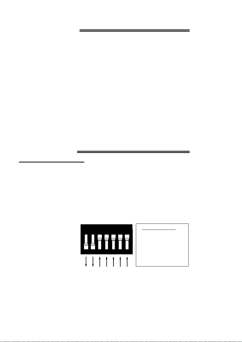
2.1 BASE ADDRESS
The PC104-DIO48 employs the PC bus for power, communications and
data transfer. As such it draws power from the PC, monitors the address
lines and control signals and responds to it's I/O address, and it receives
and places data on the eight data lines.
The base address is the starting location that software writes to and reads
from.
The base address
switch is the means for
setting the base
address. Each switch
position corresponds to
one of the PC bus
address lines. The
down position activates
that address bit.
1 2 3 4 5 6 7
BASE ADDR ESS SW ITCHES – 300h Shown.
SWITCH HEX
1 200
2 100
3 80
4 40
5 20
6 10
7 08
Figure 2-1. Base Address Switches
1
Page 6
The actual address is constructed by calculating the HEX or decimal
number Base Address Select Switches which corresponds to the base
address bits the PC104-DIO48 will respond to. For example, in Figure
2-1, switches 1 and 2 down, all others are up. Switch 1 = 200 hex (512
decimal) and switch 2 = 100 hex (256 decimal). When added together
they equal 300 hex (768 decimal).
Certain address are reserved for use by the PC (Table 2-1). Others are
free and can be used by the PC104-DIO48 and other expansion boards.
We recommend that BASE = 300 hex (768 decimal) be tried first. See
Figure 2-2 for the orientation of the switch block.
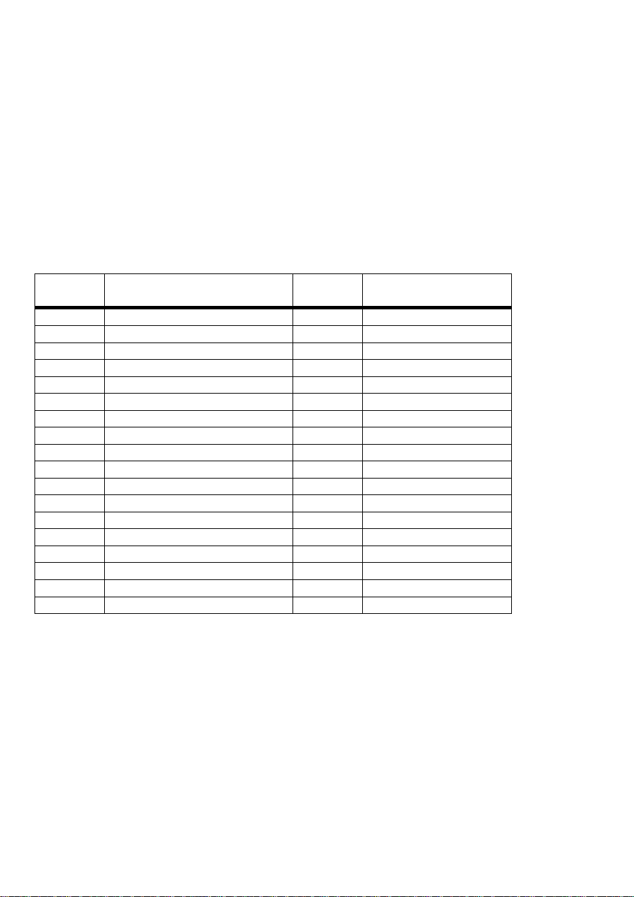
Table 2-1. PC I/O Addresses
FUNCTIONHEX
EGA2C0-2CF8237 DMA #1000-00F
EGA2D0-2DF8259 PIC #1020-021
GPIB (AT)2E0-2E78253 TIMER040-043
SERIAL PORT2E8-2EF8255 PPI (XT)060-063
SERIAL PORT2F8-2FF8742 CONTROLLER (AT)060-064
PROTOTYPE CARD300-30F
PROTOTYPE CARD310-31FDMA PAGE REGISTERS080-08F
HARD DISK (XT)320-32F8259 PIC #2 (AT)0A0-0A1
PARALLEL PRINTER378-37FNMI MASK (XT)0A0-0AF
SDLC380-38F8237 #2 (AT)0C0-0DF
SDLC3A0-3AF80287 NUMERIC CO-P (AT)0F0-0FF
MDA3B0-3BBHARD DISK (AT)1F0-1FF
PARALLEL PRINTER3BC-3BFGAME CONTROL200-20F
EGA3C0-3CFEXPANSION UNIT (XT)210-21F
CGA3D0-3DFBUS MOUSE238-23B
SERIAL PORT3E8-3EFALT BUS MOUSE23C-23F
FLOPPY DISK3F0-3F7PARALLEL PRINTER270-27F
SERIAL PORT3F8-3FFEGA2B0-2BF
RANGE
070-071
FUNCTIONHEX
RANGE
CMOS RAM & NMI MASK (AT)
The PC104-DIO48 BASE switch may be set for address in the range of
000 to 3F8 so it should not be hard to find a free address area for your
PC104-DIO48. Once again, if you are not using IBM prototyping cards
or some other board which occupies these addresses, then 300-31Fh are
free to use. Addresses not specifically listed, such as 390-39Fh, are free.
2
Page 7

2.2 INSTALLING THE BOARD
1. Turn the power off.
2. Push the board firmly down into the expansion bus connector. If it is
not seated fully it may fail to work and could short circuit the PC bus
power onto a PC bus signal. This could damage the motherboard in your
PC as well as the PC104-DIO48.
2.3 CABLING TO THE DIO48 CONNECTOR
The connector is a standard 50-pin, male, header connector. A mating
female connector (C50FF-##) may be purchased from Measurement
Computing.
2.4 SIGNAL CONNECTION
All the digital outputs/inputs on the connector are CMOS TTL. TTL is
an electronics industry term, short for Transistor Transistor Logic, which
describes a standard for digital signals which are either 0V or 5V
(nominal).
Under normal operating conditions, the voltages on the 82C55 pins
range from near 0 volts for the low state to near 5.0 volts for the high
state. Before connecting the PC104-DIO48 to external devices, review
the electrical specification in this manual to ensure that the boards input
voltage specifications are not exceeded. In addition to voltage and load
matching, digital signal sources often need to be de-bounced. More
details on digital interfacing are in the section on Interface Electronics in
this manual.
3
Page 8
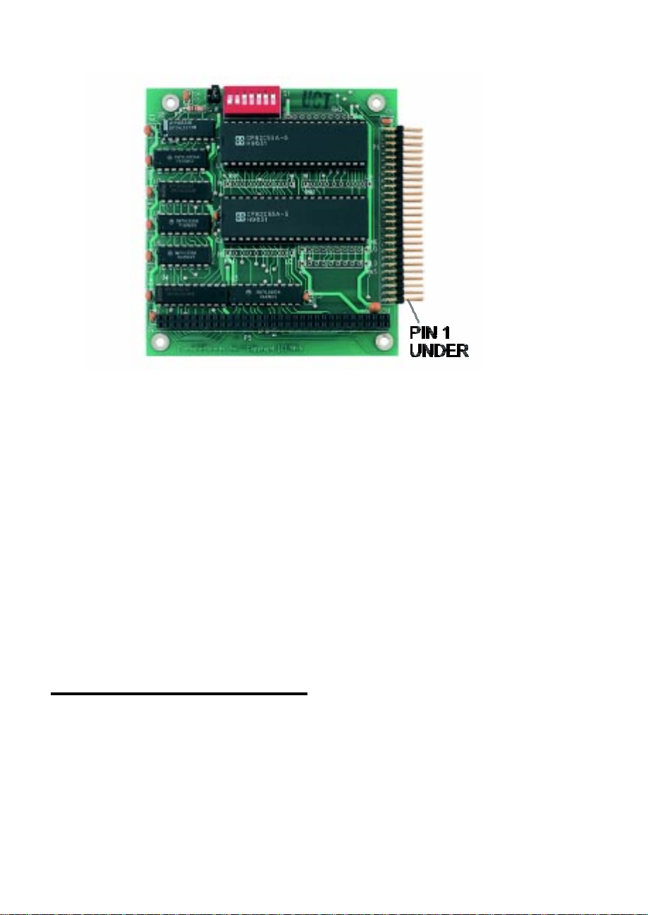
Figure 2-2. PC104-DIO48 Board Layout and Pin 1 Location
IMPORTANT NOTE: The PC104-DIO48 uses two 82C55 digital
chips for digital I/O. The 82C55 digital I/O chip initializes all ports as
inputs on power up and reset. A TTL input is a high impedance input.
If you connect another TTL input device to the 82C55 it will probably be
turned ON every time the 82C55 is reset, or, it might be turned OFF
instead. Remember, an 82C55 which is reset is in INPUT mode.
To safeguard against unwanted signal levels, all devices being controlled
by an 82C55 should be tied low (or high, as required) by a 2.2K ohm
resistor.
You will find positions for pull up and pull down resistor packs on your
PC104-DIO48 board. To implement these, please turn to the application
note on pull up/down resistors.
2.5 UNCONNECTED INPUTS
Keep in mind that unconnected inputs float. If you are using a
PC104-DIO48 board for input, and have unconnected inputs, ignore the
data from those lines.
4
Page 9

In other words, if you connect bit A0 and not bit A1, do not be surprised
if A1 stays low, stays high or tracks A0. It is unconnected and so, is not
specified. The 82C55 is not malfunctioning. In the absence of a
pull-up/down resistor, any input which is unconnected is unspecified.
You do not have to tie input lines, and unconnected lines will not affect
the performance of connected lines. Just make sure that you mask out
any unconnected bits in software.
2.6 CONNECTOR DIAGRAM
The connector accepts female 50-pin header connectors, such as those
on the C50FF-2, a 2-foot cable with connectors.
If frequent changes to signal connections or signal conditioning is
required, please refer to the information on the CIO-TERM100,
CIO-SPADE50 and CIO-MINI50 screw terminal boards.
BASE + 0, 1, 2
BASE + 4, 5, 6
Figure 2-2 I/O Connector
5
Page 10

3 CONTROL & DATA REGISTERS
We recommend that you use the Universal Library for all high level
programming. The following is basic information on the 82C55 control
and data registers and a table of control bytes for MODE 0 only. To
learn more about the other 82C55 modes, you will need the component
data book available from the component manufacturer.
Each PC104-DIO48 has two 82C55 parallel I/O chips. Each chip
contains three data and one control register occupying four consecutive
I/O address locations. The number of I/O locations occupied by a
PC104-DIO48 board is equal to 4 times the number of 82C55 chips on
the board or eight total.
The first address, or BASE ADDRESS, is determined by setting a bank
of switches on the board.
The register descriptions follow all follow the format:
01234567
A0A1A2A3A4A5A6A7
The numbers along the top row are the bit positions within the 8-bit byte
and the numbers and symbols in the bottom row are the functions
associated with each bit.
To write to or read from a register in decimal or HEX, the bit weights in
Table 2-1 apply:
Table 3-1. Bit Weights
HEX VALUEDECIMAL VALUEBIT POSITION
110
221
442
883
10164
20325
40646
801287
To write a control word or data to a register, the individual bits must be
set to 0 or 1 then combined to form a byte. Data read from registers
must be analyzed to determine which bits are on or off.
6
Page 11

The method of programming required to set/read bits from bytes is
beyond the scope of this manual. It is covered in most Introduction To
Programming books.
Board registers and their function are listed on the following table. Each
register has eight bits which may be one byte of data or they may be
eight individual read/write functions.
Table 3-2. Board I/O Addresses
WRITE FUNCTIONREAD FUNCTIONADDRESS
Port A Output (1st 8255) Port A Input of 1st 82C55BASE + 0
Port B OutputPort B InputBASE + 1
Port C OutputPort C InputBASE + 2
BASE + 3
82C55
BASE + 7
82C55
Configure 1st 82C55None. No read back on
Port A Output (2nd 8255)Port A Input of 2nd 82C55BASE + 4
Port B OutputPort B InputBASE + 5
Port C OutputPort C InputBASE + 6
Configure 2nd 82C55None. No read back on
3.1 DIGITAL I/O REGISTERS
PORT A DATA
BASE ADDRESS + 0 (1st 82C55)
BASE ADDRESS + 4 (2nd 82C55)
01234567
A0A1A2A3A4A5A6A7
PORT B DATA
BASE ADDRESS + 1 (1st 82C55)
BASE ADDRESS + 5 (2nd 82C55)
01234567
B0B1B2B3B4B5B6B7
Ports A & B may be programmed as input or output. Each is written to
and read from in bytes, although for control and monitoring purposes,
individual bits are typically used.
7
Page 12

Bit set/reset and bit read functions require that unwanted bits be masked
out of reads and ORed into writes.
PORT C DATA
BASE ADDRESS + 2 (1st 82C55)
BASE ADDRESS + 6 (2nd 82C55)
01234567
C1C2C3C4C5C6C7C8
PCL0PCL1PCL2PCL3PCH0PCH1PCH2PCH3
Port C can be used as one 8-bit port of either input or output, or it can be
split into two 4-bit ports which can be independently input or output.
The notation for the upper 4-bit port is PCH3 - PCH0, and for the lower,
PCL3 - PCL0.
Although it can be split, every read and write to port C carries eight bits
of data so unwanted information must be ANDed out of reads, and
writes must be ORed with the current status of the other port.
OUTPUT PORTS
In 82C55 mode 0 configuration, ports configured for output hold the
output data written to them. This output byte may be read back by
reading a port configured for output.
INPUT PORTS
In 82C55 mode 0 configuration, ports configured for input read the state
of the input lines at the moment the read is executed, transitions are not
latched.
For information on modes 1 (strobed I/O) and 2 (bi-directional strobed
I/O), refer to an Intel or AMD data book, 82C55 data sheet.
82C55 CONTROL REGISTERS
BASE ADDRESS + 3 (1st 82C55)
BASE ADDRESS + 7 (2nd 82C55)
01234567
CLBM1CUAM2M3MS
Group BGroup A
8
Page 13

The 82C55 can be programmed to operate in Input/ Output (mode 0),
Strobed Input/ Output (mode 1) or Bi-Directional Bus (mode 2).
Information on programming the 82C55 in mode 0 is included here.
Those wishing to use the 82C55 in modes 1 or 2, must procure a data
sheet from Intel Corporation Literature Department. Visit their web site
to obtain this data sheet.
When the PC is powered up or RESET, the 82C55 is reset. This places
all 24 lines in Input mode and no further programming is needed to use
the 24 lines as TTL inputs.
To program the 82C55 for other modes, the following control code byte
must be assembled into an 8-bit byte.
MS = Mode Set. 1 = mode set active
M3 M2 Group A Function
0 0 Mode 0Input / Output
0 1 Mode 1Strobed Input / Output
1 X Mode 2Bi-Directional Bus
A B CL CH Independent Function
1111Input
0000Output
M1 = 0 is mode 0 for group B. Input / Output
M1 = 1 is mode 1 for group B. Strobed Input / Output
The Ports A, B, C-High, and C-Low, can be independently programmed
for input or output.
The two groups of ports, group A and group B, may be independently
programmed in one of several modes. The most commonly used mode is
mode 0, input/output mode. The codes for programming the 82C55 in
mode 0 are listed in Table 2-3.
9
Page 14

Table 2-3. Mode 0 - Port I/O Select Codes
NOTE: D7 is always 1; D6, D5, and D2 are always 0.
CLBCUADECHEXD0D1D3D4
OUTOUTOUTOUT128800000
INOUTOUTOUT129811000
OUTINOUTOUT130820100
ININOUTOUT131831100
OUTOUTINOUT136880010
INOUTINOUT137891010
OUTININOUT1388A0110
INININOUT1398B1110
OUTOUTOUTIN144900001
INOUTOUTIN145911001
OUTINOUTIN146920101
ININOUTIN147931101
OUTOUTININ152980011
INOUTININ153991011
OUTINININ1549A0111
ININININ1559B1111
10
Page 15

4 SPECIFICATIONS
Power consumption
+5V Operating 130 mA typical, 200 mA max
Digital Input / Output
Digital Type 82C55
Configuration 4 ports of 8, 4 ports of 4,
programmable by port as input or
output
Number of channels 48 I/O
Output High 3.0 volts min @ −2.5 mA
Output Low 0.4 volts max @ 2.5 mA
Input High 2.0 volts min, +5.5 volts absolute max
Input Low 0.8 volts max, −0.5 volts absolute min
Power-up / reset state Input mode (high impedance)
Miscellaneous Locations provided for installation of
pull-up or pull-down resistors.
Environmental
Operating temperature range 0 to 50°C
Storage temperature range −20 to 70°C
Humidity 0 to 90% non-condensing
11
Page 16

5 ELECTRONICS AND INTERFACING
This brief introduction to the electronics most often needed by digital
I/O board users covers the following subjects:
y
Pull-up/pull-down resistors
y
Transistors
y
Power MOSFETs
y
Solid State Relays
y
Voltage dividers
y
Low pass filters for digital inputs
y
Noise; sources and solutions
IMPORTANT NOTE:
WHEN AN 82C55 IS POWERED ON OR IS
RESET, ALL PINS ARE SET TO HIGH
IMPEDANCE INPUT.
The implication of this is that if you have output devices such as solid
state relays, they may be switched on whenever the computer is powered
on or reset. To prevent unwanted switching and to drive all outputs to a
known safe state after power-on or reset, pull all pins either high (to
+5VDC ) or low (to GND) through a 2.2K ohm resistor.
To install pull up/down resistor packs, refer to the following application
note.
5.1 PULL UP & PULL DOWN RESISTORS
This section deals with pull up/pull down resistors and 82C55 digital I/O
chips.
Whenever the 82C55 is powered-on or reset, the control register is set to
a known state; that state is mode 0, all ports set to inputs.
When used as an output device to control other TTL input devices, the
82C55 applies a voltage level of near 0V for low and near 5V for high.
12
Page 17

The concept of voltage level of an 82C55 in input mode is meaningless.
Do not connect a volt meter to the floating input of an 82C55. It will
show you nothing of meaning. In input mode the 82C55 is in 'high Z' or
high impedance. If your 82C55 were connected to another input chip
(the device you were controlling), the inputs of that chip are left floating
whenever the 82C55 is in input mode.
If the inputs of the device you are controlling are left to float, they may
float up or down. The direction they float depends on the characteristics
of the circuit and is unpredictable! This is why it often appears that the
82C55 has gone high after power-up. The result can be that your
controlled device gets turned on! This is why you need pull up/pull
down resistors.
Figure 4-1 shows an 82C55 digital output with a pull-up resistor
attached.
The pull-up resistor
provides a reference to
+5V while its value of
2,200 ohms allows about
2.3 mA to flow through
the circuit.
If the 82C55 is reset and
enters high impedance
input mode, the line is
pulled high. At that point,
both the 82C55 AND the
device being controlled Figure 5-1. Output Being Pulled Up
will “see” a high signal.
If the 82C55 is in output mode, the 82C55 has enough power to override
the pull-up resistor's high signal and drive the line low. If the 82C55
asserts a high signal, the pull-up resistor guarantees that the line goes to
high (about +5V).
Of course, a pull-down resistor accomplishes the same task except that
the line is pulled low when the 82C55 is reset. The 82C55 has more
than enough power to drive the line high.
13
Page 18

The board is equipped with positions for pull-up/down resistors Single
Inline Packages (SIPs). The positions are marked RN1 through RN6 and
are located beside the 82C55s.
A 2.2K ohm, 8-resistor SIP is made of eight, 2.2K resistors. One side of
each resistor are all connected to a common point. The other ends go to
eight SIP pins. The common line, at one end of the SIP, is marked with a
dot or a line.
The SIP may be installed as pull-up or pull-down. At each location,
RN1 - RN6, there are 10 holes in a line. One end of the line is marked
“HI”, the other end is marked “LO”. The eight holes in the middle are
connected to the eight lines of a port, A, B, or C. To ‘pull up’ the digital
lines for a particular port, install the SIP resistor with the marked end
toward the ‘HI’ label. To pull down the digital lines for a particular
port, install the SIP resistor with the marked end toward the ‘LO’ label.
Install and solder the SIP in place.
A resistor value of 2.2K is recommended. Use other values only if you
have calculated the necessity of doing so.
5.2 TTL TO SOLID STATE RELAYS
Many applications require digital outputs to switch AC and DC voltage
motors on and off and to monitor AC and DC voltages. These AC and
high DC voltages cannot be controlled or read directly by the TTL
digital lines of a PC104-DIO48.
Solid State Relays, such as those available from Measurement
Computing Corp. allow control and monitoring of AC and high DC
voltages and can provide 750V isolation. Solid State Relays (SSRs) are
the recommended devices for interfacing to AC and high DC signals.
The most convenient way to use solid state relays with a PC104-DIO48
board is to purchase a Solid State Relay Rack. A SSR Rack is a circuit
board with output buffer chips which are powerful enough to switch the
SSR. It provides sockets for SSRs.
SSR Racks are available from the Measurement Computing Corporation.
If you only want to drive one or two SSRs, all you need is a 74LS244
output buffer chip between the 82C55 output and the SSR. Of course
the SSR will need a 5 volt power source as well.
14
Page 19

5.3 VOLTAGE DIVIDERS
If you wish to measure a signal which varies over a range greater than
the input range of a digital input, a proper voltage divider will drop the
voltage of the input signal to a safe level.
A voltage divider takes advantage of Ohm's law, which states,
Voltage = Current * Resistance
and Kirkoff's voltage law which states,
The sum of the voltage drops around a circuit will be equal to
the voltage drop for the entire circuit.
Implied in the above is that any variation in the voltage drop for the
circuit as a whole will have a proportional variation in all the voltage
drops in the circuit.
In a voltage divider, the voltage across one of the resistors in a circuit is
proportional to the ratio of that resistor to the total resistance in the
circuit.
Therefore, you setup a voltage divider choosing two resistors with the
proper proportions relative to the full scale of the voltage input and the
maximum signal voltage to the board.
Figure 5-2. Voltage Divider
15
Page 20

Dropping the voltage proportionally is called attenuation. The formula
for attenuation is:
The variable Attenuation is the proportional
Attenuation = R1 + R2
R2
2 = 10K + 10K
10K
difference between the signal voltage max and
the full scale of the analog input.
For example, if the signal varies between 0 and
20 volts and you wish to measure that with an
analog input with a full scale range of 0 to 10
volts, the Attenuation is 2:1 or just 2.
R1 = (A-1) * R2
For a given attenuation, pick a handy resisitor
and call it R2, the use this formula to calculate
R1.
Digital inputs may also require the use of voltage dividers. For example,
if you wish to measure a digital signal that is at 0 volts when off and 24
volts when on, you cannot connect that directly to the digital inputs. The
voltage must be dropped to 5 volts max when on. The attenuation is
24:5 or 4.8. Use the equation above to find an appropriate R1 if R2 is
1K. Remember that a TTL input is 'on' when the input voltage is greater
than 2.5V but less than 5.0V.
IMPORTANT NOTE: The resistors, R1 and R2, are
going to dissipate power in the divider circuit according
to the equation, Current = Voltage / Resistance And
power (watts) is current-squared times resistance
2
*R). The higher the value of the resistance (R1 +
(W=I
R2) the less power dissipated by the divider circuit.
Here is a simple rule:
For Attenuation of 5:1 or less, no resistor should be less
than 10K.
For Attenuation of greater than 5:1, no resistor should
be less than 1K.
16
Page 21

5.4 LOW PASS FILTERS DE-BOUNCE INPUTS
A low pass filter is placed on the signal wires between a signal and an
DIO board. It attenuates frequencies greater than the cut-off frequency
preventing them from entering the digital inputs.
The key term in a low pass filter circuit is cut-off frequency. The cut-off
frequency is that frequency above which no variation of voltage with
respect to time may enter the circuit. For example, if a low pass filter
had a cut-off frequency of 30 Hz, interference associated with line
voltage (60 Hz) would be filtered out but a signal of 25 Hz would be
allowed to pass.
Also, in a digital circuit, a low pass filter might be used to “de-bounce”
(filter) an input from a switch or external relay. (Unless switch/relay
contacts are mercury-whetted, they tend to bounce briefly on closure,
generating a pulsating noise signal. This can easily lead to erroneous
counts unless filtered out.)
Figure 5-3. Low-Pass Filter
17
Page 22

A simple low-pass filter may be constructed from one resistor (R) and
one capacitor (C) (Figure 5-3). The cut-off frequency is determined
according to the formula:
Fc =
and
R = 1
1 Where π= 3.14...
2 π R C R = ohms
C = farads
Fc = cut-off frequency in cycles/second.
2π C Fc
18
Page 23

EC Declaration of Conformity
Measurement Computing Corporation
We,
product:
48-Bit Digital I/O BoardPC104-DIO48
DescriptionPart Number
to which this declaration relates, meets the essential requirements, is in conformity
with, and CE marking has been applied according to the relevant EC Directives listed
below using the relevant section of the following EC standards and other normative
documents:
, declare under sole responsibility that the
EU EMC Directive 89/336/EEC
compatibility.
EU 55022 Class B
characteristics of information technology equipment.
EN 50082-1
IEC 801-2
and control equipment.
IEC 801-3
measurements and control equipment.
IEC 801-4
equipment.
Carl Haapaoja, Director of Quality Assurance
: Electrostatic discharge requirements for industrial process measurement
: Radiated electromagnetic field requirements for industrial process
: Electrically fast transients for industrial process measurement and control
: Limits and methods of measurements of radio interference
: EC generic immunity requirements.
: Essential requirements relating to electromagnetic
Page 24

Measurement Computing Corporation
10 Commerce Way
Suite 1008
Norton, Massachusetts 02766
(508) 946-5100
Fax: (508) 946-9500
E-mail: info@mccdaq.com
www.mccdaq.com
 Loading...