

Page 1
Digital HS
User’s Manual
IOtech, Inc.
25971 Cannon Road
Cleveland, OH 44146
Phone: (440) 439-4091
Fax: (440) 439-4093
E-mail: sales@iotech.com
Internet: http://www.iotech.com
Digital HS
User’s Manual
p/n
Digital HS - 901
© 1998 by IOtech, Inc. — Printed in the United States of America
Page 2
Warranty
Your IOtech warranty is as stated on the product warranty card. You may contact IOtech by
phone, fax machine, or e-mail in regard to warranty-related issues.
Phone: (440) 439-4091, fax: (440) 439-4093, email:
sales@iotech.com
Limitation of Liability
IOtech, Inc. cannot be held liable for any damages resulting from the use or misuse of this
product.
Copyright, Trademark, and Licensing Notic e
All IOtech documentation, software, and hardware are copyright with all rights reserved. No
part of this product may be copied, reproduced or transmitted by any mechanical,
photographic, electronic, or other method without IOtech’s prior written consent. IOtech
product names are trademarked; other product names, as applicable, are trademarks of their
respective holders. All supplied IOtech software (including miscellaneous support files,
drivers, and sample programs) may only be used on one installation. You may make archival
backup copies.
FCC Statement
IOtech devices emit radio frequency energy in levels compliant with Federal Communications
Commission rules (Part 15) for Class A devices. If necessary, refer to the FCC booklet How To Identify
and Resolve Radio-TV Interference Problems (stock # 004-000-00345-4) which is available from the
U.S. Government Printing Office, Washington, D.C. 20402.
CE Notice
Many IOtech products carry the CE marker indicating they comply with the safety and emissions
standards of the European Community. As applicable, we ship these products with a Declaration of
Conformity stating which specifications and operating conditions apply.
Warnings and Cautions
Refer all service to qualified personnel. This caution symbol warns of possible personal injury or
equipment damage under noted conditions. Follow all safety standards of professional practice and the
recommendations in this manual. Using this equipment in ways other than described in this manual can
present serious safety hazards or cause equipment damage.
This warning symbol is used in this manual or on the equipment to warn of possible injury or death from
electrical shock under noted conditions.
This ESD caution symbol urges proper handling of equipment or components sensitive to damage from
electrostatic discharge. Proper handling guidelines include the use of grounded anti-static mats and wrist
straps, ESD-protective bags and cartons, and related procedures.
Specifications and Calibration
Specifications are subject to change without notice. Significant changes will be
addressed in an addendum or revision to the manual.
hardware products to published specifications. Periodic hardware calibration is not covered
under the warranty and must be performed by qualified personnel as specified in this manual.
Improper calibration procedures may void the warranty.
As applicable, IOtech calibrates its
Quality Notice
IOtech has maintained ISO 9001 certification since 1996. Prior to shipment, we thoroughly test our
products and review our documentation to assure the highest quality in all aspects. In a spirit of
continuous improvement, IOtech welcomes your suggestions.
Page 3

Introduction
1.1 General Description
The Digital488HS/32 is a high speed IEEE 488 to digital I/O interface providing the
fastest possible communication between the IEEE 488 bus and 34 TTL compatible
digital I/O lines (17 inputs and 17 outputs). Both the input lines and the output lines
have an associated pai r of h ands hak e lin es. Th e Data Avai lab le (iDAV an d oDAV fo r
input and output respectively) line is driven by the data source to indicate that the
receiver should accept new data. The Busy (iBusy and oBusy for input and output
respectively) line is driven by the receiver to indicate that the source should not send
new data. Each handshake line is switch selectable for either active high or active low
operation.
The input and output ports are separated into one 8-bit (first byte) port and one 9-bit
(second byte) port. There are two separate switch selectable operating modes for both
the input and output data ports, 8-bit and 16-bit. In the 8-bit mode, 8-bit data are
transferred to or from the second byte port with the IEEE 488 bus control line EOI as
the 9th bit. In the 16-bit mode, the first eight bits of data are transferred to or from the
first byte port followed by the next eight bits with EOI to or from the second byte
port. The user connects the external I/O device to correspond to the desired byte
ordering (most significant byte first or least significant byte first). Both input and
output ports are separately switch selectable for either active high or active low
output data operation.
The output port provides switch selection for each bit of high or low on power-on,
reset, or clear.
There are two switch enabled conditions for which the Digital488HS/32 can request
service with SRQs: Output Port Empty and Input Port Full. This status can also
determined by Parallel Poll via switch selectable responses.
Some of the control lines available are:
oClear This output line provides an active 1µSec pulse upon
detection of the IEEE 488 multiline commands DCL and
SDC. This control line is switch selectable for either active
high or active low operation.
Page 4

oTrigger This output line provides an active 1µSec pulse upon
detection of the IEEE 488 multiline command GET. This
control line is switch selectable for either active high or
active low operation.
/oReset This output line provides an active low signal for
approximately 100msec at power on and for the duration
of the time /iReset is active plus approximately 100msec.
/iReset This input line provides an external method to power-on
cycle the Digital488HS/32. When this line is low, the
/oReset line also becomes active low.
SB1 Serial Poll Bit #1. An external input to the
Digital488HS/32 serial poll register which can be read via
IEEE 488 serial polls. This condition may also be switch
selected to generate an SRQ on the IEEE 488 bus.
SB2 Serial Poll Bit #2. An external input to the
Digital488HS/32 serial poll register which can be read via
IEEE 488 serial polls. This condition may also be switch
selected to generate an SRQ on the IEEE 488 bus.
/OE The output buffers on the digital output port are placed in
tri-state when this line is in an inactive (high) state. This
allows use of the Digital488HS/32 as a bidirectional
interface, connecting the input and output port data lines
together.
Page 5

1.2 Available Accessories
Additional accessories that can be ordered for the Digital488HS/32 include:
CA-7-1 1.5 foot IEEE 488 cable
CA-7-3 6 foot shielded IEEE 488 cable
CA-7-4 6 foot reverse entry IEEE 488 cable
CN-20 Right angle IEEE 488 adapter, male and female
CN-22 IEEE 488 multi-tap bus strip, four female connectors
in parallel
CN-23 IEEE 488 panel mount feed-through connector, male
and female
DigitalHS-901 Additional Instruction Manual
1.3 Specifications
Digital I/O Capability:
included are two output and two input data handshake lines, two status bit lines, clear output, trigger
output, reset input, input END of data and output END of data lines.
Logic Levels:
Output :
Input:
Logic Sense:
VOH = 2 volts min @ IOH = -15 mA ; 3.4 volts typ @ IOH = -3 mA
V
V
VIL = 0.8 volts max
IIH = 0.02 mA max @ VIN = 2.7 volts (Data Input Lines)
IIL = -0.20 mA max @ VIN = 0.4 volts (Data Input Lines)
IIL = -0.50 mA max @ VIN = 0.4 volts (Control & Handshake Input Lines)
IIH = -0.30 mA max @ VIN = 2.7 volts (Control & Handshake Input Lines)
Switch selectable power on and Device Clear (DCL & SDC) levels on output
data lines. Switch selectable logic inversion for input data port, output data port,
input handshake lines, output handshake lines, END lines, trigger and clear lines.
*
16-bit TTL compatible inputs, 16-bit TTL compatible outputs. Also
= 0.5 volts max @ IOL = 24 mA ; 0.4 volts MAX @ IOL = 12 mA
OL
= 2 volts min
IH
Page 6

IEEE 488.1 Specification Subsets:
SH1, AH1, T6, TE0, L3, LE0, SR1, PP2, RL0, DC1, DT1, C0, E2
DIO Drivers: Tri-State drivers are used on all DIO lines except during PPAS
(Parallel Poll Active State) when open collector drivers are used.
Connector: Standard IEEE 488.1 connector with metric studs.
Data Transfer Speed: 1,000,000 bytes/sec (handshake lines connected externally
together)
SRQ: Switch selectable SRQs on Input Port Full, Output Port Empty, External
Service Bit #1 and External Service Bit #2.
Parallel Poll: Switch selectable response on Input Port Full and Output Port Empty.
General
Indicators: LEDs for Talk, Listen, SRQ, Input Port Full, Output Port Empty and Power.
Power: 105-125V or 210-250v, 50/60 Hz; 60 VA max
Environment: 0 to 50°C; 0 to 70% RH to 35°C. Linearly derate RH 3%/°C from 35° to 50°C
Dimensions: 425mm wide x 45 mm high x 203 mm deep (16.75" x 1.75" x 8")
Weight: 4.5 kg (10 lbs)
Controls: Power switch, external switch for IEEE 488 bus address, internal switches for
output data power on levels, SRQ and ist enable, output data logic sense, input
data
logic sense and logic sense for Trigger, Clear, handshake and END lines.
Supplied Accessories: Two (2) mating solder-tab I/O connectors, power cord, manual and
rack mount kit.
*Specifications Subject to Change Without Notice
*
Page 7

1.4 Abbreviations
The following IEEE 488 abbreviations may be used throughout this manual.
addr n IEEE bus address "n"
ATN Attention line
CA Controller Active
CR Carriage Return
data Data String
DCL Device Clear
GET Group Execute Trigger
GTL Go To Local
LA Listener Active
LAG Listen Address Group
LF Line Feed
LLO Local Lock Out
MLA My Listen Address
MTA My Talk Address
PPC Parallel Poll Configure
PPU Parallel Poll Unconfigure
SC System Controller
SDC Selected Device Clear
SPD Serial Poll Disable
SPE Serial Poll Enable
SRQ Service Request
TA Talker Active
TAD Talker Address
TCT Take Control
term Terminator
UNL Unlisten
UNT Untalk
* Unasserted
Page 8

Getting Started
2.1 Inspection
The Digital488HS/32 was carefully inspected, both mechanically and electrically,
prior to shipment. After receiving the Digital488HS/32, carefully unpack all items
from the shipping carton and check for any obvious signs of physical damage. Report
any such damage found to the shipping agent immediately. Retain all shipping
materials in the event that shipment back to the factory is necessary.
Every Digital488HS/32 is shipped with the following items:
Digital488HS/32 High Speed Digital I/O Interface
•
DigitalHS-901 Instruction Manual
•
• 167-0800 Accessory Kit, which includes:
CA-1 Power Cable
FU-1-.25 1/4 Amp Replacement Fuse
FE-1 Rubber Feet (4)
EN-6 Rack Ears (2)
HA-41-6 Rack Ear Screws (4)
CN-19-37 37 Pin Male Connectors (2)
CN-17-37 Hood for CN-19-37 (2)
2.2 Configuration
The Digital488HS/32 has one external eight position switch, accessible from the rear
panel, and four internal eight position configuration switches (S2, S3, S4 and S5).
Page 9
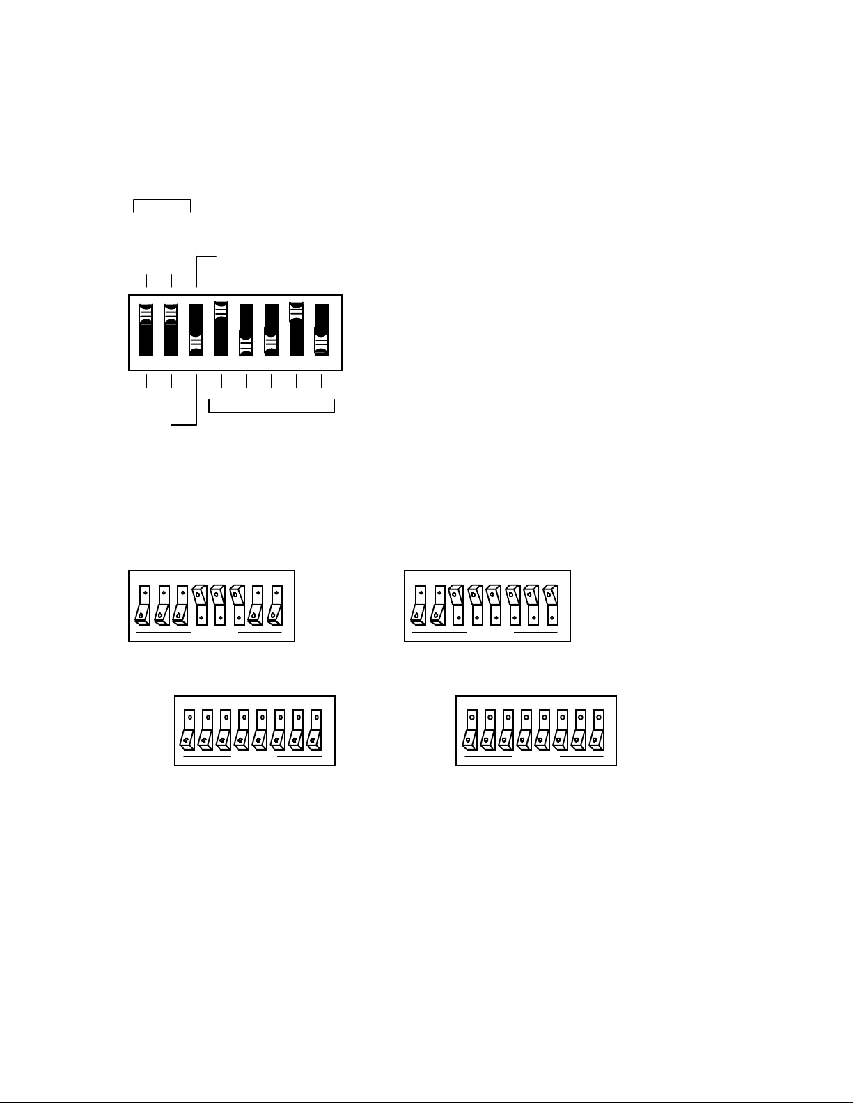
2.2.1 Factory Defaults
The Digital488HS/32 is factory configured to the following switch settings.
MODE
O
U
I
T
N
16 16
NDAC HOLDOFF ENABLE
1
1 3456782
88 168421
DIS IEEE ADDRESS
SRQ EN FULL
iDAV POL
iBUSY POL
ist EN FULL
iEND POL
iDATA POL
SRQ EN SB1
SRQ EN SB2
87654321
S2
OPEN
8
9
OUT
1 2 3 4 5 6 7 8
HI LO
PTO DEFAULT
1011121314
OPEN
15
0
S4
SRQ EN EMPTY
ist EN EMPTY
oDAV POL
oEND POL
oBUSY POL
oDATA POL
OPEN
012
OUT
1 2 3 4 5 6 7 8
HI LO
PTO DEFAULT
TRIGGER POL
CLR POL
87654321
3
4
5
6
OPEN
S3
7
S5
Page 10

2.2.2 Internal Switch Settings
The internal settings on the Digital488HS/32 are for the line voltage, input and output
settings and the PTO default settings.
WARNING
Disconnect the power cord from the ac line and
from the Digital488HS/32 prior to disassembly.
Disconnect any cables prior to disassembly.
WARNING
Never open the Digital488HS/32 case while it is
connected to the ac line. Failure to observe this
warning may result in equipment failure,
personal injury or death.
Place the interface on a flat surface. Remove the four (4) screws located at each
corner. Carefully remove the top cover. Modify the parameters appropriate for your
installation and carefully re-assemble the interface using the reverse of the procedure
described.
2.2.2.1 Line Voltage Selection
The Digital488HS/32 may be operated from 110 or 220 V ac. The unit was shipped
from the factory set for the operating voltage marked on the label placed over the
power jack on the rear panel. To change the operating voltage, change the setting ot
internal switch S7 according to the following instructions.
WARNING
The Digital488HS/32 is intended for INDOOR
USE ONLY. Failure to observe this warning
could result in equipment failure, personal
injury or death.
Page 11

1. The line voltage selection switch (S7) is located below the main power suply
transformer (T2). Insert the tip of a small screwdriver into the slot of the switch
and move the switch so the desired line voltage appears on the switch.
2. Install a power line fuse appropriate for the line voltage. The fuse is located below
the internal line voltage switch (S7). Gently pull upward on the plastic fuse
housing. Remove the entire housing with the fuse inside. Select a fuse with the
proper rating (see table below).
Line Voltage Fuse Type
105-125V 1/2A 250V, Slo Blo, 3AG
210-250V 1/4A 250V, Slo Blo, 3AG
A fuse with a rating higher than that specified
may cause damage to the instrument. If the
instrument repeatedly blows fuses, contact the
factory.
3. Open the fuse housing by pushing up on the tab on the bottom of the housing.
4. Replace the fuse and close the housing. Insert the fuse housing into the fuse
holder.
5. Make note of the new voltage setting for later reference and carefully re-assemble
the unit.
2.2.2.2 Input Setup
Several features are available for the input port. These features are selected by
internal switch S2, labeled INPUT SETUP. The factory defaults for these feature
selections are shown on the next page.
The features include:
SRQ On Input Port Full (Serial Poll Feature)
SRQ On Status Bit 1 - SB1 (Serial Poll Feature)
SRQ On Status Bit 2 - SB2 (Serial Poll Feature)
ist Enable on Input Port Full (Parallel Poll Feature)
Polarity Selection for Input Data, iEND, iD AV and iBusy Lines
Page 12
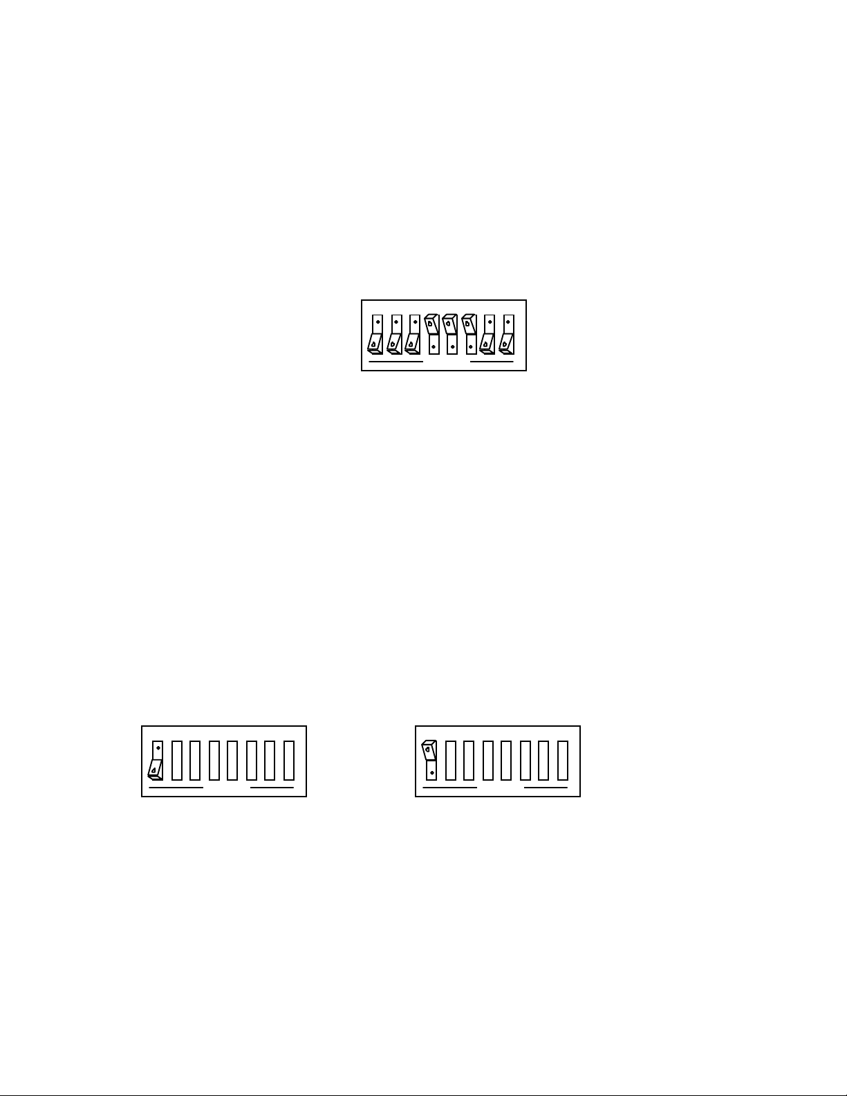
The digital input port contains 16 bits of TTL level inputs, one END line (iEND)
input, two handshake lines (iDAV and iBusy), one control line (\iRESET), two status
lines (SB1 and SB2), and logic supply lines (+5V and ground).
SRQ EN FULL
iDAV POL
iBUSY POL
ist EN FULL
iEND POL
iDATA POL
SRQ EN SB1
SRQ EN SB2
87654321
S2
OPEN
Input Port Feature Selection Switch
Default Settings
2.2.2.2.1 S2-1 SRQ EN Full: Service Request Enable
Service Request (SRQ) Enable causes the Digital488HS/32 to generate a service
request on the IEEE 488 bus when iDAV transitions from the inactive (not Full) to
the active state (Full), indicating the external device has transferred data and the port
is Full. Default is SRQ on Full disabled.
SRQ EN FULL
8
7654321
OPEN
SRQ on Full Disabled
S2
SRQ EN FULL
87654321
S2
OPEN
SRQ on Full Enabled
(default)
SRQ On Input Port Full Selection
Page 13
2.2.2.2.2 S2-2
ist
EN Full: Individual Status Message True on Input Port Full
Enable
The Full status of the input port can be sensed via parallel polls when the ist
(individual status message) Enable is selected. See section 3.4 for more information.
Default is disabled.
ist EN FULL
OPEN
ist
on Input Full Disabled
87654321
S2
ist
ist EN FULL
87654321
S2
OPEN
on Input Full Enabled
(default)
Individual Status Message (
ist
) on Full Status
2.2.2.2.3 S2-3 iDAV POL: Input Data Available Handshake Line
The Input Data available handshake line is an input line sourced by the external
device. It can be configured for rising edge or falling edge operation. Factory default
is falling edge operation.
iDAV POL
87654321
OPEN
Falling Edge iDAV
(default)
Polarity Selection for the iDAV Handshake Line
S2
iDAV POL
87654321
S2
OPEN
Rising Edge iDAV
Page 14
2.2.2.2.4 S2-4 iBUSY POL: Input Port Busy Handshake Line
The input port busy handshake line, iBusy, is an input line sourced by the
Digital488HS/32. It can be configured as active high or active low. Factory default is
active high.
iBUSY POL
87654321
OPEN
Active Low iBusy
S2
Active High iBusy
iBUSY POL
87654321
S2
OPEN
(default)
Polarity Selection for the iBusy Handshake Line
2.2.2.2.5 S2-5 iEND POL: Input End Control Line Polarity
The iEND control line is latched into the ninth bit of the second byte input port. This
latched iEND signal directly drives the IEEE 488 EOI line during the second byte
transfer and can be used to signal the end of the transfer to the IEEE 488 controller.
iEND can be set for active high or active low operation. Default is active high.
iEND POL
87654321
OPEN
Active Low iEND
S2
iEND POL
87654321
S2
OPEN
Active High iEND
(default)
Page 15

Polarity Selection for the iEND Control Line
2.2.2.2.6 S2-6 iDATA POL: Input Data Polarity
The input data bits can be active high or active low. For example, if a data byte of
&h07 is transferred from the input port with the iData Polarity selected for active low
operation, the data byte received by the IEEE 488 controller will be &hF8.
At power on, iRESET, Device Clear (DCL) or Selected Device Clear (SDC), the 16bit digital input latches are forced to a Not Full condition. Default setting is active
high.
iDATA POL
87654321
OPEN
Active Low iDATA
Polarity Selection for the Input Port Data Lines
S2
iDATA POL
87654321
S2
OPEN
Active High iDATA
(default)
Page 16
2.2.2.2.7 S2-7 and S2-8 SRQ EN SB1 and SRQ EN SB2: Service Request
on External Status Bit 1 and 2
The input port has two status line inputs that allow the external device to request
service to the IEEE 488 bus via the Digital488HS/32. Each of these status line inputs
is capable of generating an SRQ on the bus when this feature is enabled. When
enabled, a service request is generated on the rising edge of the SB signal lines. This
active polarity i s not s witch select able. Each s tatus b it can be p olled by the IEEE 488
bus controller via serial polls. The level of the signal is latched at the beginning of the
serial poll process. Default is SRQ disabled.
SRQ EN SB1
87654321
OPEN
SRQ on SB1 Disabled
(default)
SRQ On External Status Bit 1 (SB1) Selection
OPEN
S2
OPEN
SRQ on SB1 Enabled
SRQ EN SB2
87654321
S2
SRQ EN SB1
87654321
S2
SRQ EN SB2
87654321
S2
OPEN
SRQ on SB2 Disabled
(default)
SRQ on SB2 Enabled
Page 17

SRQ On External Status Bit 2 (SB2) Selection
2.2.2.3 Digital Output Port Setup
Several features are available for the output port. These features are selected by
internal switch S3, labeled OUTPUT SETUP. The factory defaults for these feature
selections are shown in the following.
The features include:
SRQ On Output Port Empty (Serial Poll Feature)
ist Enable on Output Port Empty (Parallel Poll Feature)
Polarity Selection for Output Data, oEND, oT rigger, oClear,
oDAV and oBusy Lines
The digital out put port contai ns 16 bits of TTL l evel outpu ts, one END lin e (oEND),
two handshake lines (oDAV and oBusy), four control lines (/oRESET, /OE, oClear
and oTrigger) and logic supply lines (+5V and ground).
SRQ EN EMPTY
ist EN EMPTY
oDAV POL
oBUSY POL
TRIGGER POL
oEND POL
oDATA POL
CLR POL
87654321
S3
OPEN
Output Port Feature Selection Switch
Default Settings
2.2.2.3.1 S3-1 SRQ EN EMPTY: Service Request Enable
Page 18

Service Request (SRQ) Enable causes the Digital488HS/32 to generate a service
request on the IEEE 488 bus when oBusy transitions from the active (Not Empty) to
the inactive (Empty) state, indicating the external device has accepted previous data
and the port is Empty. Default is SRQ on Empty disabled.
SRQ EN EMPTY
87654321
S3
OPEN
SRQ on Empty Disabled
SRQ EN EMPTY
87654321
S3
OPEN
SRQ on Empty Enabled
(default)
SRQ On Output Port Empty Selection
2.2.2.3.2 S3-2
ist
EN EMPTY: Individual Status Message True on Outut
Port Empty Enable
The Empty status can be sensed via parallel polls when the individual status message
(ist) enable is selected. See section 3.4 for more information. Default is disabled.
ist EN EMPTY
OPEN
ist
on Empty Disabled
87654321
S3
ist EN EMPTY
OPEN
ist
on Empty Enabled
87654321
S3
(default)
Individual Status Message (
ist
) on Output Port Empty Selection
2.2.2.3.3 S3-3 oDAV POL: Output Data Available Handshake Line
Page 19

The Output Data available handshake line, oDAV, is an output line sourced by the
Digital488HS/32. It can be configured for active high or active low operation.
Factory default is active high (rising edge) operation.
oDAV POL
87654321
OPEN
Falling Edge oDAV
S3
Rising Edge oDAV
oDAV POL
87654321
S3
OPEN
(default)
Polarity Selection for the oDAV Handshake Line
2.2.2.3.4 S3-4 oBUSY POL: Output Port Busy Handshake Line
The output port busy handshake line, oBusy, is an input sensed by the
Digital488HS/32. It can be configured as active high or active low. Factory default is
active high.
oBUSY POL
87654321
OPEN
Active Low oBusy
S3
Active High oBusy
oBUSY POL
87654321
S3
OPEN
(default)
Polarity Selection for the oBusy Handshake Line
2.2.2.3.5 S3-5 oEND POL: Output End Control Line
The level of the oEND control line is individually switch selectable for active high or
active low operation. The oEND line is forced active, either high or low, by power-
Page 20

on, iRESET, Device Clear (DCL) or Selected Device Clear (SDC). The default setting
for S3-5 is active high. The oEND is not affected by the \OE line; it is always
enabled.
oEND POL
87654321
OPEN
Active Low oEND
S3
Active High oEND
oEND POL
87654321
S3
OPEN
(default)
Polarity Selection for the oEND Control Line
2.2.2.3.6 S3-6 oDATA PO L: Output Data Polarity
The output data bits' polarity can be active high or active low. For example, if a data
byte of &h07 is transferred to the output port with oData Polarity selected for active
low operation, the levels at the output port are &hF8.
The first and second byte outport drivers are controlled by the output enable input
(/OE). In order to allow the digital output data to be presented to the output
connector, the /OE input must be forced low. The oEND output is always enabled,
regardless of the state of /OE input. This allows the input and output ports on the
Digital488HS/32 to be connected to form a bi-directional bus.
At power-on, iRESET, Device Clear (DCL) or Selected Device Clear (SDC), S3-6 is
ignored and the 16 data bits of the first and second byte ouput ports are forced to the
levels selected by the S4 and S5 switch settings. These settings are in effect until the
first data are written to the output port. The oEND output is forced active. Default of
S3-6 is active high output data bits.
Page 21

oDATA POL
87654321
oDATA POL
87654321
OPEN
Active Low oDATA
S3
OPEN
Active High oDATA
S3
(default)
Polarity Selection for the Output Port Data Lines
2.2.2.3.7 S3-7 TRIGGER POL: Output Trigger Control Line Polarity
The trigger control line may be set for active low or active high operation. Default is
active high.
OPEN
TRIGGER POL
87654321
S3
OPEN
TRIGGER POL
87654321
S3
Active Low oTrigger Active High oTrigger
(default)
Polarity Selection for the oTrigger Line
2.2.2.3.8 S3-8 CLR POL: Output Clear Control Line Polarity
The Output Clear control line can be selected for active low or active high. Default is
active high.
Page 22

CLR POL
CLR POL
87654321
87654321
S3
OPEN
OPEN
Active Low oClear Active High oClear
(default)
Polarity Selection for the oClear Line
S3
Page 23

2.2.2.4 Power-On Default Settings
Switches S4 and S5, labeled PTO Default, set the power-on default settings for the
Digital488HS/32. The power-on settings set the output port to high or low on poweron.
8
9
OUT
1 2 3 4 5 6 7 8
HI LO
PTO DEFAULT
1011121314
OPEN
15
S4
012
OUT
1 2 3 4 5 6 7 8
HI LO
PTO DEFAULT
3
OPEN
4
5
6
7
S5
Power On Default Switches for First Byte and Second Byte
At power-on, iRESET, Device Clear or Selected Device Clear, S3-6 (output data
polarity) is ignored and the digital outputs are forced to the level selected by the S4
and S5 settings. These settings are in effect until the first datum is written to the
output port. Each data line in the output port is set individually by these switches.
Factory default is all data lines low. The oEND output is forced active.
2.3 External Switches
The Digital488HS/32 has one eight position switch accessible fron the rear panel.
This switch determines the unit's IEEE 488 bus address, input and output mode, and
whether NDAC Holdoff is used. The switch is read only during power on and should
be set before applying power.
2.3.1 Input Port Mode Selection
The switch labeled MODE IN selects either 8-bit or 16-bit input port operation. In 8bit mode, 8-bit data are transferred from the second byte port with the iEND line
driving the IEEE 488 bus EOI line as the ninth bit. In 16-bit mode, the first eight bits
of data are transferred from the first byte port followed by the next eight bits with
iEND from the second byte port. The user connects the external device to correspond
to the desired byte ordering (most significant byte first or least significant byte first).
Page 24

MODE
O
U
I
T
N
16 16
NDAC HOLDOFF ENABLE
MODE
O
U
I
T
N
16 16
NDAC HOLDOFF ENABLE
1 3456782
88 168421
DIS IEEE ADDRESS
16-Bit Input Mode Selected
1
0
1 3456782
88 168421
DIS IEEE ADDRESS
8-Bit Input Mode Selected
1
0
(default)
Input Port Mode Selection Switch
2.3.2 Output Port Mode Selection
The switch labeled MODE OUT selects either 8-bit or 16-bit output port operation. In
8-bit mode, 8-bit data are transferred to the second byte port with the IEEE 488 bus
EOI line driving the oEND output. In 16-bit mode, the first eight bits of data are
transferred to the first byte port followed by the next eight bits with EOI to the second
byte port. The user connects the external device to correspond to the desired byte
ordering (most significant byte first or least significant byte first).
Page 25

MODE
O
U
I
T
N
16 16
NDAC HOLDOFF ENABLE
MODE
O
U
I
T
N
16 16
NDAC HOLDOFF ENABLE
1
1 3456782
88 168421
DIS IEEE ADDRESS
0
16-Bit Output Mode Selected
1 3456782
88 168421
DIS IEEE ADDRESS
8-Bit Output Mode Selected
1
0
(default)
Output Port Mode Selection Switch
2.3.3 NDAC Holdoff Enable/Disable
When Digital488HS/32 presents output data, it asserts the oDAV line to inform the
external device that data are available. The external device then responds by asserting
the oBusy signal to indicate that it has accepted the data. At this point, the
Digital488HS/32 unasserts oDAV and waits for the external device to unassert oBusy
in preparation for new output.
The Digital488HS/32 uses the IEEE 488 bus handshake lines to make sure data are
not sent to it faster than the external device can accept the data. Normally, the
Digital488HS/32 uses the Not Ready For Data (NRFD) data lines for this purpose.
This allows the IEEE 488 bus to continue with other activity, even though the
external device has not yet accepted the data.
When NDAC holdoff is enabled, the Digital488HS/32 uses the IEEE 488 NDAC line
to stop the IEEE 488 bus until the external device has accepted the data (as indicated
by its assertion of the oBusy line). In this way, the controller is guaranteed the data it
has sent to the Digital488HS/32 has been accepted by the external device.
When the oBusy handshake line is active, the Digital488HS/32 stops any additional
data transfers to the output port. However, the IEEE 488 bus controller can continue
to process other bus commands and control other instruments. In some cases, this
may not be des ired. The switch labeled NDAC HOLDOFF ENABLE/DIS allows the
Page 26

bus controller to be held off with the NDAC handshake line. This option is set by the
switch labeled NDAC HOLDOFF ENABLE. Factory default setting is NDAC holdoff
disabled.
MODE
O
U
I
T
N
16 16
NDAC HOLDOFF ENABLE
1
1 3456782
88 168421
DIS IEEE ADDRESS
0
NDAC Holdoff Disabled NDAC Holdoff Enabled
NDAC Holdoff Enable Selection
2.3.4 IEEE 488 Address Selection
MODE
O
U
I
T
N
16 16
1 3456782
88 168421
DIS IEEE ADDRESS
NDAC HOLDOFF ENABLE
1
0
Digital488HS/32's IEEE 488 bus address is set by the switches labeled IEEE
ADDRESS on the rear panel of the unit. The address can be set from 0 through 30.
The address is selected by simple binary weighting, with the switch labeled 1 being
the least significant bit and the switch labeled 16 the most significant bit. The factory
default is address 18. If address 31 is selected, the interface is placed in the “Listen
Only” or “Listen Always” mode.
Page 27

1
1 3456782
168421
IEEE Address = 18
0
0 x 1
1 x 2
0 x 4
0 x 8
1 x 16
=0
=2
=0
=0
+ =16
IEEE Bus Address Selection
2.4 IEEE 488 Bus Implementation
The Digital488HS/32 implements many of the capabilities defined by the IEEE 488.1
specification. These are discussed in the following sections. The bus uniline and
multiline commands the Digital488HS/32 does not support or respond to include the
following:
Remote Enable (REN) Parallel Poll Configure (PPC)
Go to Local (GTL) Parallel Poll Unconfigure (PPU)
Local Lockout (LLO) Parallel Poll Disable (PPD)
Take Control (TCT)
2.4.1 My Talk Address (MTA)
When the Digital488HS/32 is addressed to talk, it outputs any data available on the
Digital Input Port. If the interface has been Serial Poll Enabled (SPE) by the
controller, it responds with its serial poll status byte until Serial Poll Disabled (SPD).
2.4.2 My Listen Address (MLA)
When the Digital488HS/32 is addressed to listen, it accepts characters from the active
talker and outputs them without interpretation to the Digital Output Port. The
Digital488HS/32 is not software programmable, so it does not accept any device
dependent commands.
Page 28

2.4.3 Device Clear (DCL and SDC)
In response to a DCL or SDC from the IEEE488 bus, the Digital488HS/32 pulses the
oClear control line for 1µsec. In addition, the input port is forced Empty and the
output port is forced to its power-on default value. For more information, see PTO
default switches,S4 and S5.
2.4.4 Group Execute Trigger (GET)
When the Digital488HS/32 recognizes a GET, the Digital488HS/32 pulses the
oTrigger control line for 1µsec.
2.4.5 Interface Clear (IFC)
IFC places the Digital488HS/32 in the Talker/Listener Idle State.
2.4.6 Serial Poll Enable (SPE)
When Serial Poll Enabled (SPE), the Digital488HS/32 sets itself to respond to a serial
poll with its serial poll status byte if addressed to talk. When the serial poll byte is
accepted by the controller, any pending SRQs are cleared. The Digital488HS/32
continues to try to output its serial poll response until it is Serial Poll Disabled (SPD)
by the controller.
2.4.7 Serial Poll Disable (SPD)
Disables the Digital488HS/32 from responding to serial polls by the controller.
2.4.8 Unlisten (UNL)
Unlisten (UNL) places the Digital488HS/32 in the Listener Idle State.
2.4.9 Untalk (UNT)
Page 29

Untalk (UNT) places the Digital488HS/32 in the Talker Idle State.
2.4.10 Serial Poll Response
Whenever the Digital488HS/32 generates a service request (SRQ), a serial poll by the
controller returns a serial poll status byte of at least 64 (decimal) showing the SRQ
was generated by the Digital488HS/32. For more information, see section 3.3.
2.4.11 Parallel Poll Response
The Digital488HS/32 outputs its individual status message (ist) on the IEEE 488 bus
data line determined by the setting of the three least significant bus address switches
(IEEE Address 1, 2, 4). For examp le, with the factory d efault address of 18, the data
line chosen is DIO3 (data bit line 2). See section 3.4 for more information
2.5 Front Panel Indicators
Six indicator lights on the front panel of the Digital488HS/32 display the status of the
interface. The function of each indicator is described below.
POWER On when power is applied to the Digital488HS/32 and the power switch
on the back panel is depressed. Off if power is not present.
TALK On when the Digital488HS/32 is in the IEEE 488 Talker state,
off when the Digital488HS/32 is in the Idle or Listener state.
LISTEN On when the Digital488HS/32 is in the IEEE 488 Listener state,
off when the Digital488HS/32 is in the Idle or Talker state.
SRQ On when the Digital488HS/32 has generated an IEEE 488 service request
(SRQ), off when no SRQ from the Digital488HS/32 is pending.
Page 30

EMPTY On when the Digital488HS/32's output data port is Empty,
indicating the external device has accepted the output data, off when the
output port is Not Empty.
FULL On when the Digital488HS/32 has accepted data on the Input Data Port
from the external device. Off when no input port data is pending (that is,
Not Full).
Page 31

Operation
1192
+
1
891
S
212
3.1 Digital Output Port
The digital out put port contai ns 16 bits of TTL l evel outpu ts, one END lin e (oEND),
two handshake lines (oDAV and oBusy), four control lines (/oRESET, /OE, oClear
and oTrigger) and logic supply lines (+5V and ground).
oEND
oDAV
oBusy
oRESET
oTrigger
oClear OE
17
18
19
6
37
36
35 34
DOUT15 - DOUT0
First Byte
33
Common
econd Byte
037
0
5 volts
Digital Output Port Connector Pinouts
Output Port Organization
Second ByteFirst Byte
15 14 13 12 11 10 9 8 7 6 5 4 3 2 1 0 oEND
First Byte, Second Byte and oEND Bit Organization
In 16-bit mode, both the first byte and second byte ports are changed simultaneously,
that is, without respect to the IEEE 488 bus data transfer rate. The first byte is first
transferred into a holding latch. When the second byte is accepted by the
Digital488HS/32, then the first byte data are transferred from the holding register to
the output register. The following simplified block diagram illustrates this output
transfer.
Page 32

Internal
Data Bus
First Byte
Clock
Second Byte
Clock
First
Byte
Holding
Register
First
Byte
Output
Register
Second
Byte
Output
Register
DOUT8
thru
DOUT15
DOUT0
thru
DOUT7
EOI
1 bit Reg
oEND
Simplified Output Port Block Diagram
3.1.1 Output Port Data Lines
The first and second byte output port drivers are externally controlled. The Output
Enable control line (/OE) must be forced low to allow the digital output data to be
presented on the output connector. If /OE is disconnected or forced high, the output
drivers are disabed and the output connector is not driven. This allows the input and
output ports on the Digital488HS/32 to be connected to form a bidirectional bus. The
oEND output, however, is always enabled. /OE does not affect the oEND control
line.
The Output Enable control line (/OE) places the output port buffers, both first and
second byte, into tri-state operation if left floating or forced active high. To enable the
output port, this line must be driven active low. The state of the /OE line does not
effect the oEND control line. This allows the input and output ports to be used as a
bi-directional interface, connecting the input and output port data lines together.
The IEEE 488 (EOI) End or Identify bus control line is often used to designate the
last byte of a multiple byte transfer. The Digital488HS/32 latches the EOI signal into
the ninth bit (oEND) of the second byte output port. This oEND signal, derived
directly from the EOI line, can be used to signal the end of the transfer to the external
device.
Page 33

3.1.2 Output Port Handshake Lines (oDAV and oBusy)
The Output Data Available (oDAV) han dshake line is an outp ut line sourced by the
Digital488HS/32. The Output Port Busy (oBusy) handshake line is an input that is
sensed by the Digital488HS/32.
Data are not written to the output port while oBusy input is active. When oBusy
becomes inactive, all 17 bits of data, including oEND, are presented to the output
lines. 125 ns later, oDAV is forced active. In the 8-bit mode the first byte port content
is not specified.
Once the external device has sensed the assertion of oDAV, it must latch the data and
then assert oBusy for at least 150 ns. The external device must unassert oBusy when
it is ready for more data.
First Byte
Second Byte
oEnd
>125 ns
oDAV
oBusy
1) When oBusy input line is unasserted, the Digital488HS/32 puts data on the
output port.
2) The Digital488HS/32 waits at least 125 ns, then asserts oDAV.
3) The external device should then assert oBusy and latch the data.
4) oBusy must remain asserted until 150 ns have elapsed or oDAV becomes
unasserted.
5) The external device unasserts oBusy preparing for next transfer.
Output Port Timing Diagram
Page 34

3.1.2.1 NDAC Holdoff Selection
The Digital488HS/32 stops any additional data transfers to the output port while the
oBusy handshake line is active, indicating the connected external device has not
accepted the previous data provided by the oDAV transition. It does this by not
releasing the NRFD IEEE 488 bus handshake line, thus indicating its “Not Ready for
Data” condition.
Even though the Digital488HS/32 is not ready, the IEEE 488 bus controller can
continue to process other bus commands and control other instruments. Occasionally,
such as when a trigger command is to be issued, it is desirable to prohibit the bus
controller from processing other bus commands until the output data have been
accepted by the external device.
In this example, the bus controller may be able to output data to the Digital488HS/32
and issue the trigger faster than the external device can accept the output port data. If
trigger must be synchronized with the data transfer, it would be necessary to serial
poll or parallel poll the Digital488HS/32 to determine if the data have been
transferred.
Aternatively, the Digital488HS/32 can stop the IEEE 488 bus controller until the data
have been accepted by the external device. It does so by leaving NDAC asserted until
the external device has accepted the output data. Since every data byte on the IEEE
488 bus must be accepted (for example, with an NDAC transition) the bus is not
allowed to continue until the Digital488HS/32 releases NDAC.
3.1.3 oClear Control Line
When the Digital488HS/32 detects a Device Clear (DCL) or a Selected Device Clear
(SDC) IEEE 488 bus command, it generates a 1µsec pulse on the oClear control line.
3.1.4 oTrigger Control Line
When the Digital488HS/32 detects the Group Execute Trigger (GET) IEEE 488 bus
command, it generates a 1µsec pulse on the oTrigger control line.
Page 35

3.1.5 /oRESET Control Line
The /oRESET control line is an active low signal that follows the internal reset line of
the Digital488HS/32. During power-on or external application of a low input to the
/iRESET line, this line remains in the low state for approximately 120 to 150 ms.
There is no selection for polarity for this control line.
3.1.6 Logic Supply Lines
The +5 V connection provides five volts for use by external circuits. Care must be
taken to assure that the external circuit does not draw more than 100mA.
3.1.7 Data Transfer Speed Considerations
The data transfer speeds on the IEEE 488 bus are affected by both the IEEE 488 bus
talker and the IEEE 488 bus listener. In fact, the data on the bus can only transfer as
fast as the slowest listener. The Digital488HS/32 is capable of accepting bus data for
transfer to the output port at greater than 1,000,000 bytes per second. The data
acceptance time (time between falling edge of DAV to rising edge of NDAC) is
approximately 200 ns. This allows the IEEE talker 800 ns on its part of the handshake
to meet the 1,000,000 bytes per second transfer speed.
3.2 Digital Input Port
The digital input port contains 16 bits of TTL level inputs, one END line (iEND)
input, two handshake lines (iDAV and iBusy), one control line (/iRESET), two status
lines (SB1 and SB2) and logic supply lines (+5V and ground).
Page 36

iEND
iDAV
iBusy
iRESET
SB2
SB1
17
18
19
37
36
35
DIN15 - DIN0
Second ByteFirst Byte
34 21
Common
18916
119
2037
20
+5 volts
Digital Input Port Connector Pinouts
Input Port Organization
DIN0 Thru DIN15
Second ByteFirst Byte
15 14 13 12 11 10 9 8 7 6 5 4 3 2 1 0 iEND
First Byte, Second Byte and iEND Bit Organization
Both the first byte and second byte port data are latched simultaneously on the active
edge of the iDAV handshake line.
3.2.1 Input Port Handshake Lines (iDAV and iBusy)
Data to the input port should not be written while the handshake line, iBusy, is active.
When sensed inactive, all 17 bits of data can be presented to the input lines followed
by a minimum delay of 50 ns, after which iDAV can be forced active.
The leading transition of the iDAV line latches data into the input latches. The iBusy
signal, when active, causes subsequent leading edge transitions of iDAV to be
ignored until the iBusy signal becomes inactive. When iDAV senses active, iBusy is
forced active until all data have been transferred to the IEEE 488 bus listener. The
iDAV line must then go inactive for a minimum duration of 150 ns following the
inactive state of iBusy before additional data can be detected on the input port.
Page 37

First Byte
Second Byte
oEnd
iDAV
iBusy
1) The external device waits for iBusy to be unasserted.
2) The external device presents data to the input port.
3) After at least 50 ns, the external device asserts iDAV until 150 ns have passed
4) The external device unasserts iDAV until at least 150 ns after iBusy is
or until iBusy is asserted.
unasserted.
Input Port Timing Diagram
>50 ns
>150 ns
3.2.2 /iRESET Control Line
The /iRESET control line provides a method by which the external device can force a
power-on reset of the Digital488HS/32. This line, normally pulled high by an internal
10k• pull-up resistor, causes the power-on reset sequence when forced to a low state.
The polarity (active level) of this control line is not switch selectable. iReset must be
held active for at least 2 ms to ensure proper reset.
3.2.3 Logic Supply Lines
Provisions have been made to allow the external device to be powered by the
Digital488HS/32 internal 5 volt logic supply. Care must be taken to assure that the
external circuit does not draw greater than 100 mA total (50 mA to each port).
3.2.4 Data Transfer Speed Considerations
The data transfer speeds on the IEEE 488 bus are affected by both the IEEE 488 bus
talker and the IEEE 488 bus listener. In fact, the data on the bus can only transfer as
Page 38

fast as the slowest listener. The Digital488HS/32 is capable of transmitting bus data
at a rate greater than 1,000,000 bytes per second.
3.3 Serial Polling
The Digital488HS/32 can provide internal and external status in addition to
generating requests for service via the SRQ IEEE 488 control line. The following
shows the status bit positions contained within the Serial Poll Byte Status Register.
Serial Poll Byte
Bit Assignments
DIO8 DIO7 DIO6 DIO5 DIO4 DIO3 DIO2 DIO1
0
rsv
00
SB2 SB1 FULLEMPTY
These status bits include:
DIO1 FULL The input port is Full.
Data may be read from the input port.
DIO2 EMPTY The output port is Empty.
Data may be written to the output port.
DIO3 SB1 External Status Bit #1 input.
Level Sensitive Bit. Rising edge SRQ generating if
enabled.
DIO4 SB2 External Status Bit #2 input.
Level Sensitive Bit. Rising edge SRQ generating if
enabled.
DIO5 Not Used Always 0.
DIO6 Not Used Always 0.
DIO7 rsv Reserved Bit. Indicates the Digital488HS/32 caused
the SRQ.
DIO8 Not Used Always 0.
Page 39

3.4 Parallel Polling
The Digital488HS/32 provides the method by which the individual status message
(ist), either "true" (1) or "false" (0), can be determined by parallel poll.
ist is set true or false according to the setting of the ist EN Full switch (S2-2), the ist
EN Empty switch (S3-2), and the current states of the input and output ports. The
three least significant address IEEE 488 bus address switches (labeled 1, 2 and 4)
determine which bus DIO line the Digital488HS/32 uses to report the status. The
following table illustrates the Address Switch, ist status and the DIO line used.
IEEE Bus Address Switch Status Parallel Poll Response
–
–
–
–
–
–
–
–
–
–
–
–
–
–
–
–
–
–
–
0
0
0
0
1
1
1
1
–
0
0
1
1
0
0
1
1
ist
–
0
1
0
1
0
1
0
1
0
1
1
1
1
1
1
1
1
DIO8 DIO7 DIO6 DIO5 DIO4 DIO3 DIO2 DIO1S1-4 S1-5 S1-6 S1-7 S1-8
0
0
0
0
0
0
0
0
1
0
0
0
0
0
0
0
1
0
0
0
0
0
0
0
1
0
0
0
0
0
0
0
1
0
0
0
0
0
0
0
1
0
0
0
0
0
0
0
1
0
0
0
0
0
0
0
1
0
0
0
0
0
0
0
1
0
0
0
0
0
0
0
The following table shows the status enable switch settings, the status conditions and
the corresponding individual status message (ist).
EN Empty S3-2
ist
Disabled
Enabled
Enabled
Disabled
Disabled
Enabled
Enabled
Enabled
Enabled
Output
–
Empty
Not Empty
–
–
Empty
Empty
Not Empty
Not Empty
EN Full S2-2
ist
Disabled
Disabled
Disabled
Enabled
Enabled
Enabled
Enabled
Enabled
Enabled
Input
–
–
–
Full
Not Full
Full
Not Full
Full
Not Full
ist
ist
0
1
0
1
0
1
1
1
0
Page 40

IEEE 488 Primer
4.1 HISTORY
The IEEE 488 bus is an instrumentation communication bus adopted by the Institute
of Electrical and Electronic Engineers in 1975, revised in 1978 and revised and
extended in 1987. The Digital488HS/32 conforms to this most recent revision
designated IEEE 488.1.
Prior to the adoption of this standard, most instrumentation manufacturers offered
their own versions of computer interfaces. This placed the burden of system hardware
design on the end user. If his application required the products of several different
manufacturers, then he might need to design several different hardware and software
interfaces. The popularity of the
urpose Interface Bus or
P
mechanical interface as well as the data transfer and control protocols. The use of the
IEEE 488
interface to design of the high level software that is specific to the measurement
application.
standard has moved the responsibility of the user from design of the
GPIB
IEEE 488
) is due to the total specification of the electrical and
interface (sometimes called the General
4.2 GENERAL STRUCTURE
The main purpose of the
or more devices. A device can either be an instrument or a computer. Before any
information transfer can take place, it is first necessary to specify which will do the
talking (send data) and which devices will be allowed to listen (receive data). The
decision of who will talk and who will listen usually falls on the
which is, at power on, the
The
System Controller
committee, only one person may speak at a time and the chairman is responsible for
recognizing members and allowing them to have their say. On the bus, the device
which is recognized to speak is the
time if the information transferred is to be clearly understood by all. The act of
"giving the floor" to that device is called
chairman can not attend the meeting, or if other matters require his attention, he can
appoint an acting chairman to take control of the proceedings. For the
device becomes the
At a committee meeting, everyone present usually listens. This is not the case with
the
GPIB
other devices to ignore what is being transmitted. A device is instructed to listen by
. The
Active Controller
IEEE 488.1
Active Controller
is similar to a committee chairman. On a well run
Active Controller
interface is to transfer information between two
System Controller
.
Active Talker
Addressing to Talk
.
selects which devices will listen and commands all
. There can only be one Talker at a
. If the committee
GPIB
, this
Page 41

being
Addressed to Listen
. This device is then referred to as an
Devices which are to ignore the data message are instructed to
Active Listener
Unlisten
.
.
The reason some devices are instructed to
Unlisten
is quite simple. Suppose a
college instructor is presenting the day's lesson. Each student is told to raise their
hand if the instructor has exceeded their ability to keep up while taking notes. If a
hand is raised, the instructor stops his discussion to allow the slower students the time
to catch up. In this way, the instructor is certain that each and every student receives
all the information he is trying to present. Since there are a lot of students in the
classroom, this exchange of information can be very slow. In fact, the rate of
information transfer is no faster than the rate at which the slowest note-taker can keep
up. The instructor, though, may have a message for one particular student. The
instructor tells the rest of the class to ignore this message (
Unlisten
) and tells it to
that one student at a rate which he can understand. This information transfer can then
happen much quicker, because it need not wait for the slowest student.
The
GPIB
called
For data transfer on the
a)
b) Designate who will
c) Designate all the devices who are to
devices to
transfers information in a similar way. This method of data transfer is
handshaking
Unlisten
. More on this later.
IEEE 488
, the
Active Controller
all devices to protect against eavesdroppers.
listen
by
talk
addressing
.
a device to
listen
by
talk
addressing
must…
.
those
d) Indicate to all devices that the data transfer can take place.
Page 42

Device 1
System Controller
Able to Talk,
Listen, and Control
Device 2
DMM
Able to Talk
and Listen
Device 3
Printer
Only Able to Listen
To Other Devices
Data Bus
Data Byte
Transfer
Control
General
Interface
Management
Device 4
Frequency Counter
Only Able to Talk
IEEE 488 Bus Structure
4.3 SEND IT TO MY ADDR ESS
DIO1-8
}
DAV
NRFD
NDAC
IFC
ATN
SRQ
REN
EOI
Page 43

In the previous discussion, the terms
Addressed to Talk
were used. These terms require some clarification.
and
Addressed to Listen
The
IEEE 488.1
standard permits up to 15 devices to be configured within one
system. Each of these devices must have a unique address to avoid confusion. In a
similar fashion, every building in town has a unique address to prevent one home
from receiving another home's mail. Exactly how each device's address is set is
specific to the product's manufacturer. Some are set by DIP switches in hardware,
others by software. Consult the manufacturer's instructions to determine how to set
the address.
Addresses are sent with
Controller
Address
. These commands include
(MTA),
Talk Address Group
universal
(
multiline
) commands from the
My Listen Address
(TAG), and
Listen Address Group
(MLA),
Active
My Talk
(LAG).
4.4 BUS MANAGEMENT LINES
Five hardware lines on the
lines are often referred to as
GPIB
are used for bus management. Signals on these
uniline
(single line) commands. The signals are active
low, i.e. a low voltage represents a logic "1" (asserted), and a high voltage represents
a logic "0" (unasserted).
4.4.1 Attention (ATN)
is one of the most important lines for bus management. If Attention is asserted,
ATN
then the information contained on the data lines is to be interpreted as a multiline
command. If it is not, then that information is to be interpreted as data for the
Listener
s. The
Active Controller
is the only bus device that has control of this line.
Active
Page 44

4.4.2 Interface Clear (IFC)
The
devices in a known state. Although device configurations vary, the
usually places the devices in the Talk and Listen Idle states (neither
nor
Active Listener
line is used only by the
IFC
).
System Controller
. It is used to place all bus
command
IFC
Active Talker
4.4.3 Remote Enable (REN)
When the
System Controller
remote operation. Generally, the
programming is attempted. Only the
Enable
line.
sends the
REN
System Controller
command, bus devices will respond to
REN
command should be issued before any bus
has control of the
Remote
4.4.4 End or Identify (EOI)
The
that is sending the data asserts
line is used to signal the last byte of a multibyte data transfer. The device
EOI
during the transfer of the last data byte. The
EOI
EOI
signal is not always necessary as the end of the data may be indicated by some special
character such as carriage return.
The
Active Controller
asserting
EOI
and
also uses
ATN
to perform a
EOI
Parallel Poll
by simultaneously
.
4.4.5 Service Request (SRQ)
When a device desires the immediate attention of the
. It is then the Controller's responsibility to determine which device requested
SRQ
service. This is accomplished with a
Serial Poll
or a
Active Controller
Parallel Poll
.
it asserts
Page 45

4.5 HANDSHAKE LINES
The
GPIB
uses three handshake lines in an "I'm ready - Here's the data - I've got it"
sequence. This handshake protocol assures reliable data transfer, at the rate
determined by the slowest Listener. One line is controlled by the Talker, while the
other two are shared by all Active Listeners. The handshake lines, like the other
IEEE 488
lines, are active low.
4.5.1 Data Valid (DAV)
The
DAV
line is controlled by the
Talker
. The
Talker
verifies that
NDAC
is asserted
(active low) which indicates that all Listeners have accepted the previous data byte
transferred. The
Talker
then outputs data on the bus and waits until
NRFD
is
unasserted (high) which indicates that all Addressed Listeners are ready to accept the
information. When
( active low) to indicate that the data on the bus is valid.
DAV
NRFD
and
NDAC
are in the proper state, the
Talker
asserts
4.5.2 Not Ready for Data (NRFD)
This line is used by the
new data. The
Talker
Listeners
must wait for each
to inform the
Listener
Talker
when they are ready to accept
to unassert this line (high) which
they will do at their own rate when they are ready for more data. This assures that all
devices that are to accept the information are ready to receive it.
4.5.3 Not Data Accepted (NDAC)
The
NDAC
line is also controlled by the
Listeners
. This line indicates to the
Talker
that each device addressed to listen has accepted the information. Each device
releases
NDAC
(high) at its own rate, but the
NDAC
will not go high until the
slowest Listener has accepted the data byte.
Page 46

DIO1-8
(composite)
1st Data Byte 2nd Data Byte
DAV
Source
NRFD
Acceptor
NDAC
Acceptor
Ready
Accept
Valid Not
All
None
None
Ready
Accept
All
Valid
All
Ready
None
Accept
Valid
Not
Valid
None
Ready
All
Accept
IEEE Bus Handshaking
4.6 DATA LINES
The
GPIB
eight data lines use the convention of
provides eight data lines for a bit parallel/byte serial data transfer. These
DIO1
through
DIO8
instead of the binary
designation of D0 to D7. The data lines are bidirectional and are active low.
4.7 MULTILINE COMMANDS Multiline
ATN
(bus) commands are sent by the
Active Controller
asserted. These commands include addressing commands for talk, listen, Untalk
over the data bus with
and Unlisten.
4.7.1 Go To Local (GTL)
This command allows the selected devices to be manually controlled. ($01)
4.7.2 Listen Address Group (LAG)
There are 31 (0 to 30) listen addresses associated with this group. The 3 most
significant bits of the data bus are set to 001 while the 5 least significant bits are the
address of the device being told to listen.
4.7.3 Unlisten (UNL)
Page 47

This command tells all bus devices to Unlisten. The same as Unaddressed to Listen.
($3F)
4.7.4 Talk Address Group (TAG)
There are 31 (0 to 30) talk addresses associated with this group. The 3 most
significant bits of the data bus are set to 010 while the 5 least significant bits are the
address of the device being told to talk.
4.7.5 Untalk (UNT)
This command tells bus devices to Untalk. The same as Unaddressed to Talk. ($5F)
4.7.6 Local Lockout (LLO)
Issuing the
($11)
4.7.7 Device Clear (DCL)
This command causes all bus devices to be initialized to a pre-defined or power up
state. ($14)
4.7.8 Selected Device Clear (SDC)
This causes a single device to be initialized to a pre-defined or power up state. ($04)
command prevents manual control of the instrument's functions.
LLO
Page 48

4.7.9 Serial Poll Disable (SPD)
The
command disables all devices from sending their Serial Poll status byte.
SPD
($19)
4.7.10 Serial Poll Enable (SPE)
A device which is Addressed to Talk will output its Serial Poll status byte after
is sent and
is unasserted. ($18)
ATN
SPE
4.7.11 Group Execute Trigger (GET)
This command usually signals a group of devices to begin executing a triggered
action. This allows actions of different devices to begin simultaneously. ($08)
4.7.12 Take Control (TCT)
This command passes bus control responsibilities from the current
Controller
to
another device which has the ability to control. ($09)
4.7.13 Secondary Command Group (SCG)
These are any one of the 32 possible commands (0 to 31) in this group. They must
immediately follow a talk or listen address. ($60 to $7F)
4.7.14 Parallel Poll Configure (PPC)
This configures devices capable of performing a
they are to assert in response to a
Parallel Poll
. ($05)
Parallel Poll
as to which data bit
Page 49

4.7.15 Parallel Poll Unconfigure (PPU)
This disables all devices from responding to a
Parallel Poll
. ($15)
4.8 MORE ON SERVICE REQUESTS
Most of the commands covered, both uniline and multiline, are the responsibility of
the
Active Controller
to send and the bus devices to recognize. Most of these
happen routinely by the interface and are totally transparent to the system
programmer. Other commands are used directly by the user to provide optimum
system control. Of the uniline commands,
is very important to the test system
SRQ
and the software designer has easy access to this line by most devices. Service
Request is the method by which a bus device can signal to the
Controller
that an
event has occurred. It is similar to an interrupt in a microprocessor based system.
Most intelligent bus peripherals have the ability to assert
. A DMM might assert
SRQ
it when its measurement is complete, if its input is overloaded or for any of an
assortment of reasons. A power supply might
This is a powerful bus feature that removes the burden from the
to periodically inquire, "Are you done yet?". Instead, the
if its output has current limited.
SRQ
System Controller
Controller
says, "Do what
I told you to do and let me know when you're done" or "Tell me when something is
wrong."
Since
is a single line command, there is no way for the
SRQ
Controller
to determine
which device requested the service without additional information. This information
is provided by the multiline commands for
Serial Poll
and
Parallel Poll
.
4.8.1 Serial Poll
Suppose the
Controller
there are several devices which could assert
receives a service request. For this example, let's assume
SRQ
. The
Controller
issues an
SPE
(Serial Poll enable) command to each device sequentially. If any device responds
with DIO7 asserted it indicates to the
. Often times the other bits will indicate why the device wanted service. This
SRQ
Serial Polling
sequence, and any resulting action, is under control of the software
Controller
that it was the device that asserted
designer.
Page 50

4.8.2 Parallel Poll
The
Parallel Poll
is another way the
Controller
can determine which device
requested service. It provides the who but not necessarily the why. When bus devices
are configured for Parallel Poll, they are assigned one bit on the data bus for their
response. By using the Status bit, the logic level of the response can be programmed
to allow logical OR/AND conditions on one data line by more than one device. When
is asserted, the
SRQ
Controller
must then analyze the eight bits of data received to determine the source
Controller
of the request. Once the source is determined, a
(under user's software) conducts a
Serial Poll
might be used to
Parallel Poll
. The
determine the why.
Of the two polling types, the
Serial Poll
determine the who and why. In addition, most devices support
is the most popular due to its ability to
Serial Poll
only.
Page 51

$00 $10 $20 $30 $40 $50 $60 $70
$01 $11 $21 $31 $41 $51 $61 $71
GTL LLO
$02 $12 $22 $32 $42 $52 $62 $72
$03 $13 $23 $33 $43 $53 $63 $73
$04 $14 $24 $34 $44 $54 $64 $74
SDC DCL
$05 $15 $25 $35 $45 $55 $65 $75
PPC PPU
$06 $16 $26 $36 $46 $56 $66 $76
$07 $17 $27 $37 $47 $57 $67 $77
$08 $18 $28 $38 $48 $58 $68 $78
GET SPE
$09 $19 $29 $39 $49 $59 $69 $79
TCT SPD
$0A $1A $2A $3A $4A $5A $6A $7A
$0B $1B $2B $3B $4B $5B $6B $7B
$0C $1C $2C $3C $4C $5C $6C $7C
$0D $1D $2D $3D $4D $5D $6D $7D
$0E $1E $2E $3E $4E $5E $6E $7E
$0F $1F $2F $3F $4F $5F $6F $7F
0
NUL
SOH
STX
ETX
EOT
ENQ
ACK
BEL
BS
HT
LF
VT
FF
CR
SO
SI
DLE
1
DC1
2
DC2
3
DC3
4
DC4
5
NAK
6
SYN
7
ETB
8
CAN
9
EM
10
SUB
11
ESC
12
FS
13
GS
14
RS
15
US
ACG UCG
16
17
18
19
20
21
22
23
24
25
26
27
28
29
30
31
00
01
02
03
04
05
06
07
08
09
10
11
12
13
14
15
32
SP
16
33
!
17
34
"
18
35
#
19
36
$
20
37
%
21
38
&
22
39
'
23
40
(
24
41
)
25
42
*
26
43
+
27
44
,
28
45
-
29
46
.
30
47
/
UNL
48 64 80 96 112
0
1
2
3
4
5
6
7
8
9
:
;
<
=
>
?
49
50
51
52
53
54
55
56
57
58
59
60
61
62
63
00
01
02
03
04
05
06
07
08
09
10
11
12
13
14
15
@
A
B
C
D
E
F
G
H
K
L
M
N
O
P
16
65
SCG
81
Q
17
66
SCG
82
R
18
67
SCG
83
S
19
68
SCG
84
T
20
69
SCG
85
U
21
70
SCG
86
V
22
71
SCG
87
W
23
72
SCG
88
X
24
73
I
25
74
J
26
75
SCG
89
Y
SCG
90
Z
SCG
91
[
27
76
SCG
92
\
28
77
SCG
93
]
29
78
SCG
94
^
30
79
SCG
95
_
UNT
SCG
LAG TAG SCG
`
SCG
97
a
SCG
98
b
SCG
99
c
SCG
100
d
SCG
101
e
SCG
102
f
SCG
103
g
SCG
104
h
SCG
105
i
SCG
106
j
SCG
107
k
SCG
108
l
SCG
109
m
SCG
110
n
SCG
111
o
SCG
p
113
q
114
r
115
s
116
t
117
u
118
v
119
w
120
x
121
y
122
z
123
{
124
|
125
}
126
~
127
DEL
ACG = Addressed Command Group
UCG = Universal Command Group
LAG = Listen Address Group
TAG = Talk Address Group
SCG = Secondary Command Group
Page 52

oEND
oDAV
oBusy
oRESET
oTrigger
oClear OE
17
18
19
37
36
35 34
First Byte
33 21
DOUT15 - DOUT0
Second Byte
Common
Digital Output Port Connector
18916
119
2037
20
+5 volts
iEND
iDAV
iBusy
iRESET
SB2
SB1
17
18
19
37
36
35
DIN15 - DIN0
Second ByteFirst Byte
34 21
Common
Digital Input Port Connector
18916
119
2037
20
+5 volts
Page 53

Pin Description DirectionDesignation
Digital Output Port Connector Pin Assignments
1
2
3
4
5
6
7
8
9
10
11
12
13
14
15
16
17
18
19
20
21
22
23
24
25
26
27
28
29
30
31
32
33
34
35
36
37
DOUT0
DOUT1
DOUT2
DOUT3
DOUT4
DOUT5
DOUT6
DOUT7
DOUT8
DOUT9
DOUT10
DOUT11
DOUT12
DOUT13
DOUT14
DOUT15
oEND
oDAV
oBusy
+5v
Common
Common
Common
Common
Common
Common
Common
Common
Common
Common
Common
Common
Common
/OE
oClear
oTrigger
/oRESET
Bit 0
Bit 1
Bit 2
Bit 3
Bit 4
Bit 5
Bit 6
Bit 7
Bit 8
Bit 9
Bit 10
Bit 11
Bit 12
Bit 13
Bit 14
Bit 15
End Of Transfer Bit
Output Data Available
Output Busy
Logic Power
Logic Common
Logic Common
Logic Common
Logic Common
Logic Common
Logic Common
Logic Common
Logic Common
Logic Common
Logic Common
Logic Common
Logic Common
Logic Common
Output Tri-State Enable
Output Clear
Output Trigger
Output Reset
Second
Byte
First
Byte
Output - Tri-state
Output - Tri-state
Output - Tri-state
Output - Tri-state
Output - Tri-state
Output - Tri-state
Output - Tri-state
Output - Tri-state
Output - Tri-state
Output - Tri-state
Output - Tri-state
Output - Tri-state
Output - Tri-state
Output - Tri-state
Output - Tri-state
Output - Tri-state
Output
Output
Input
+Vcc
Ground
Ground
Ground
Ground
Ground
Ground
Ground
Ground
Ground
Ground
Ground
Ground
Ground
Input
Output
Output
Output
Page 54

Pin Description DirectionDesignation
Digital Input Port Connector Pin Assignments
1
2
3
4
5
6
7
8
9
10
11
12
13
14
15
16
17
18
19
20
21
22
23
24
25
26
27
28
29
30
31
32
33
34
35
36
37
DIN0
DIN1
DIN2
DIN3
DIN4
DIN5
DIN6
DIN7
DIN8
DIN9
DIN10
DIN11
DIN12
DIN13
DIN14
DIN15
iEND
iDAV
iBusy
+5v
Common
Common
Common
Common
Common
Common
Common
Common
Common
Common
Common
Common
Common
Common
SB1
SB2
/iRESET
Bit 0
Bit 1
Bit 2
Bit 3
Bit 4
Bit 5
Bit 6
Bit 7
Bit 8
Bit 9
Bit 10
Bit 11
Bit 12
Bit 13
Bit 14
Bit 15
End Of Transfer Bit
Input Data Available
Input Busy
Logic Power
Logic Common
Logic Common
Logic Common
Logic Common
Logic Common
Logic Common
Logic Common
Logic Common
Logic Common
Logic Common
Logic Common
Logic Common
Logic Common
Logic Common
Status Bit #1
Status Bit #2
Input Reset
Second
Byte
First
Byte
Input
Input
Input
Input
Input
Input
Input
Input
Input
Input
Input
Input
Input
Input
Input
Input
Input
Input
Output
+Vcc
Ground
Ground
Ground
Ground
Ground
Ground
Ground
Ground
Ground
Ground
Ground
Ground
Ground
Ground
Input
Input
Input
Page 55

The following example uses the Digital488HS/32 as an IEEE 488 to Parallel
(Centronics) converter. It uses only the output port in 8-bit mode. The IEEE 488 bus
address of the Digital488HS/32 is assumed to be 08. This simple example could be
expanded to include error reporting of the parallel BUSY, PAPER and /ERROR
signals. All it attempts to do, however, is print a text file, "TEST.DAT," to the
parallel printer.
To begin, construct this cable:
19
118
Output Port
Connector
oDAV-18
oBusy-19
D0-1
D1-2
D2-3
D3-4
D4-5
D5-6
D6-7
D7-8
1
20
21-GND
22-GND
23-GND
24-GND
25-GND
26-GND
27-GND
28-GND
29-GND
30-GND
31-GND
34-/OE
35-oClear
GND-19
GND-20
GND-21
GND-22
GND-23
GND-24
GND-25
GND-26
GND-27
GND-28
GND-29
GND-30
RESET-31
1 STROBE
2-D0
3-D1
4-D2
5-D3
6-D4
7-D5
8-D6
9-D7
10-ACK
Parallel
(Centronics)
Connector
19
37
36
Cable Wiring - Digital488HS/32 to Parallel Cable
Page 56

The Digital488HS/32 must be set up with the following switch defaults:
S1-2 Closed 8-bit Output Port Mode
S1-3 Closed NDAC Holdoff Disabled
S1-4-8 Various IEEE 488 Bus Address = 18
S3-6 Open Active High Data
S3-4 Closed Active Low Level oBusy
S3-3 Closed Falling Edge iDAV
S3-8 Closed Active Low oClear
This program is used to transfer the ASCII text file to the Digital488HS/32 using the
IOtech Personal488 Controller package. Connect the Digital488HS/32 to the printer
with the fabricated cable. Enter this simple program and print.
*
* Sample Program - IEEE 488 to Parallel Converter
* Using the IOtech Model Digital488HS/32
* October 22, 1991
*
* Initialize Driver488
10 OPEN "\DEV\IEEEOUT" FOR OUTPUT AS #1
20 IOCTL#1,"BREAK"
30 PRINT#1,"RESET"
40 OPEN "\DEV\IEEEIN" FOR INPUT AS #2
* Open the test file for printing
50 OPEN "TEST.DAT" FOR INPUT AS #3
* Reset the Parallel Printer
60 PRINT#1,"CLEAR08"
* Now output the data from the test file
70 WHILE NOT EOF(3)
80 LINE INPUT#3,A$
90 PRINT#1,"OUTPUT08;";A$
100 WEND
110 CLOSE
 Loading...