

Page 1

Digital488/80A User's Manual
80-Bit IEEE 488 / Digital I/O Interface
the smart approach to instrumentation ™
IOtech, Inc.
25971 Cannon Road
Cleveland, OH 44146-1833
Phone: (440) 439-4091
Fax: (440) 439-4093
E-mail:
Internet: www.iotech.com
Digital488/80A User's Manual
80-Bit IEEE 488 / Digital I/O Interface
p/n 196-0901 Rev 1.2
Released Per EO # 1941R5
sales@iotech.com
© 1998 through 2004 by IOtech, Inc. 967695 Printed in the United States of America.
Page 2
Warranty Information
Your IOtech warranty is as stated on the product warranty card. You may contact IOtech by phone,
fax machine, or e-mail in regard to warranty-related issues.
Phone: (440) 439-4091, fax: (440) 439-4093, e-mail: sales@iotech.com
Limitation of Liability
IOtech, Inc. cannot be held liable for any damages resulting from the use or misuse of this product.
Copyright, Trademark, and Licensing Notice
All IOtech documentation, software, and hardware are copyright with all rights reserved. No part of this product may be
copied, reproduced or transmitted by any mechanical, photographic, electronic, or other method without IOtech’s prior
written consent. IOtech product names are trademarked; other product names, as applicable, are trademarks of their
respective holders. All supplied IOtech software (including miscellaneous support files, drivers, and sample programs)
may only be used on one installation. You may make archival backup copies.
CE Notice
Many IOtech products carry the CE marker indicating they comply with the safety and emissions standards of the
European Community. As applicable, we ship these products with a Declaration of Conformity stating which
specifications and operating conditions apply.
Warnings, Cautions, Notes, and Tips
Refer all service to qualified personnel. This caution symbol warns of possible personal injury or equipment damage
under noted conditions. Follow all safety standards of professional practice and the recommendations in this manual.
Using this equipment in ways other than described in this manual can present serious safety hazards or cause equipment
damage.
This warning symbol is used in this manual or on the equipment to warn of possible injury or death from electrical
shock under noted conditions.
This ESD caution symbol urges proper handling of equipment or components sensitive to damage from electrostatic
discharge. Proper handling guidelines include the use of grounded anti-static mats and wrist straps, ESD-protective
bags and cartons, and related procedures.
This symbol indicates the message is important, but is not of a Warning or Caution category. These notes can be of
great benefit to the user, and should be read.
In this manual, the book symbol always precedes the words “Reference Note.” This type of note identifies the location
of additional information that may prove helpful. References may be made to other chapters or other documentation.
Tips provide advice that may save time during a procedure, or help to clarify an issue. Tips may include additional
reference.
Specifications and Calibration
Specifications are subject to change without notice. Significant changes will be addressed in an addendum or revision to
the manual. As applicable, IOtech calibrates its hardware to published specifications. Periodic hardware calibration is
not covered under the warranty and must be performed by qualified personnel as specified in this manual. Improper
calibration procedures may void the warranty.
Quality Notice
IOtech has maintained ISO 9001 certification since 1996. Prior to shipment, we thoroughly test our products and
review our documentation to assure the highest quality in all aspects. In a spirit of continuous improvement, IOtech
welcomes your suggestions.
Page 3
Introduction to this Manual
This manual covers the setup and operation of the Digital488/80A 80-bit IEEE 488 / Digital I/O interface
system. This manual is organized as follows:
• Chapter 1 - Digital488/80A Overview gives an overview of the basic features of a Digital488/80A
system. Digital488/80A accessories and specifications are also provided.
• Chapter 2 - Digital488/80A Setup explains in detail the various hardware features of the
Digital488/80A unit.
• Chapter 3 - Digital488/80A Power & Assembly provides detailed instructions on line-voltage
selection and fuse replacement, rack-mount and bench-top installation, as well as power-up activation.
• Chapter 4 - Digital488/80A Operation explains the Digital488/80A internal operation. Descriptions
of the handshaking/control lines, as well as IEEE 488 bus support, are provided.
• Chapter 5 - IEEE 488 Background describes the history and the basic concepts of IEEE 488
operation, including the various IEEE 488 bus lines and bus commands.
• Chapter 6 - Digital488/80A Commands discusses the entire command set covering the
Digital488/80A unit. The command syntax, groups, and reference are provided. The description
format of the individual commands includes the command type, syntax, description, and an example
program excerpt.
• Chapter 7 - Troubleshooting provides a reference for possible solutions to technical problems. Before
calling for technical assistance, refer to this chapter.
• Appendix A provides the Digital488/80A HVCX1 Configuration Record for recording hardware and
software settings, and recording DB-50 connector wiring information.
• Appendix B provides background information concerning the IEEE 488 bus, the serial bus, and ASCII
controls.
• The Index provides a comprehensive alphabetical listing of the main terms and topics in this manual.
Also, the Abbreviations on the last pages of this manual, provides an overall list of abbreviations,
including acronyms and ASCII control codes, as an additional reference for this manual and for other
related literature.
CAUTION
Using this equipment in ways other than described in this manual can cause personal
injury or equipment damage. Before setting up and using your equipment, you should
read all documentation that covers your system. Pay special attention to cautions and
warnings formatted like this one.
Digital488/80A User’s Manual i
Page 4

Table of Contents
1 - Digital488/80A Overview
Introduction…… 1
Addressing Modes…… 1
Digital I/O Lines…… 1
Handshaking/Control Lines…… 1
HVCX1 High Voltage/Current Interface
Option…… 2
Power-Up & Setup Configuration…… 2
Internal Buffer…… 2
Software Programmable Features…… 2
Accessories…… 2
Specifications…… 3
Digital I/O…… 3
IEEE 488…… 3
General…… 3
Data Transfer Speeds…… 4
2 - Digital488/80A Setup
The Package…… 5
Hardware Setup…… 6
Front & Rear Panel Layouts…… 6
Default DIP Switch Settings…… 7
IEEE 488 Bus Address Selection…… 7
Addressing Mode Selection…… 7
Dual Primary Addressing Mode…… 8
Secondary Addressing Mode…… 8
HVCX1 Option Setup…… 10
Determining Ports Setup…… 11
To Set Up Input Ports…… 12
To Set Up Handshaking Input Lines…… 13
To Set Up Output Ports…… 14
To Set Up Handshaking Output Lines…… 14
To Install the HVCX1 Option…… 16
Digital I/O Ports…… 17
Using the HVCX1 Option for High Voltage/Current
Options…… 18
3 - Digital488/80A Power & Assembly
Introduction…… 19
Internal Components…… 19
Factory Service…… 19
Power Line & Fuse Configuration…… 20
Line Voltage Selection…… 20
To Select the Line Voltage…… 21
Fuse Replacement…… 22
To Replace the Fuse…… 22
Rack-Mount & Bench-Top Assembly…… 23
Rack Mount…… 23
Bench Top…… 23
Power-Up & Programming Tests…… 24
Power-Up Activation…… 24
Programming Examples……25
KYBDCTRL.BAS Program…… 25
To Run the Keyboard Controller Program…… 25
Digital488/80A Command Responses…… 26
4 - Digital488/80A Operation
Introduction…… 29
Handshaking/Control Lines…… 29
Clear (Pin 41)…… 30
Data Strobe (Pin 42)…… 30
Trigger (Pin 43)…… 30
Inhibit (Pin 44)…… 31
Service (Pin 45)…… 31
External Data Ready (Pin 46)…… 31
IEEE 488 Bus Support…… 32
Bus Lines…… 32
Bus Commands…… 32
Bus Addresses…… 34
Bus Terminators…… 34
5 - IEEE 488 Background
History…… 35
General Bus Structure…… 35
Bus Lines & Bus Commands…… 36
Bus Management Lines…… 36
Handshake Lines…… 37
Data Transfer Lines…… 37
Bus Command Groups…… 38
More On Service Requests…… 39
6 - Digital488/80A Commands
Introduction…… 41
Command Syntax…… 42
Command Set & Support…… 43
Command Summary…… 44
Command Reference…… 46
A - Bit Set…… 47
B - Bit Clear…… 48
C - Configuration…… 49
D - Data Output…… 50
E? - Query Error Status…… 51
F - Data Format…… 53
G - Bus Input/Output…… 57
H - Handshake…… 58
I - Invert…… 59
K - End-Or-Identify…… 60
L - Buffer…… 61
M - Service Request Mask…… 62
O - Recall Configuration…… 63
P - Port Select…… 64
Q - Inhibit…… 65
R - Data Ready…… 66
S - Save Configuration…… 67
T - Test…… 68
U - User Status…… 69
V - View Configuration…… 72
V? - View Version…… 73
X - Execute…… 74
Y - Bus Terminator…… 75
? - Query…… 76
Serial Poll Status Byte…… 77
ii Digital488/80A User’s Manual
Page 5

7 - Troubleshooting
Radio Interference Problems…… 79
Electrostatic Discharge (ESD) Damage……
79
Other Issues…… 79
Power-Up Activation…… 79
Buffer Overrun…… 80
Query Error Status…… 80
A - Appendix A
Digital488/80A HVCX1 Configuration
Record…… 81
Hardware Setup…… 81
Software Setup…… 82
DB-50 Connector Wiring Reference…… 83
B - Appendix B
IEEE 488 Bus & Serial Bus Lines…… 81
IEEE 488 Bus Commands…… 86
ASCII Codes…… 87
ASCII Code Summary…… 87
Decimal Values 00 to 63 - ACG, UCG & LAG……
87
Decimal Values 64 to 127 - TAG & SCG…… 88
ASCII Code Details…… 89
Decimal Values 00 to 31 - ACG & UCG
Characteristics…… 89
Decimal Values 00 to 31 - ACG & UCG
Descriptions…… 90
Decimal Values 32 to 63 - LAG…… 91
Decimal Values 64 to 95 - TAG…… 92
Decimal Values 96 to 127 - SCG…… 93
Index…… 95
Abbreviations…… 98
Digital488/80A User’s Manual iii
Page 6

Notes
iv Digital488/80A User’s Manual
Page 7

Digital488/80A Overview 1
Introduction…… 1
Addressing Modes…… 1
Digital I/O Lines…… 1
Handshaking/Control Lines…… 1
HVCX1 High Voltage/Current Interface Option…… 2
Power-Up & Setup Configuration…… 2
Internal Buffer…… 2
Software Programmable Features…… 2
Accessories…… 2
Specifications…… 3
Digital I/O…… 3
IEEE 488…… 3
General…… 3
Data Transfer Speeds…… 4
Introduction
The Digital488/80A is a digital input and output interface to the IEEE 488 bus that enables an IEEE 488
controller to program 80 bits of TTL level signals as either inputs or outputs. It includes six
handshake/control lines for each 40-bit channel and two addressing modes. The unit is fully
programmable, including the power-up configuration, which is stored in non-volatile RAM. The internal
data buffer in the Digital488/80A can store up to 2,000 40-byte words. With the addition of the HVCX1
High Current/High Voltage Interface option, the I/O lines can be configured as high voltage inputs or as
high current/high voltage outputs to allow interfacing with solenoids, switching relays and other high
voltage/high current devices.
Addressing Modes
Two addressing modes are available in the Digital488/80A. Dual primary addressing permits two channels
to reside at two consecutive primary IEEE 488 bus addresses. Secondary addressing allows two channels
to reside at the same primary IEEE 488 bus address with two consecutive secondary addresses.
When addressed to Talk, the Digital488/80A outputs data from all forty bits of the selected channel or a
selected eight bit port. When addressed to Listen, the unit accepts input data and programming information
from the controller and outputs the data to the appropriate I/O port.
Digital I/O Lines
The Digital488/80A has 80 TTL level digital I/O lines that are divided into two 40-bit channels. Each
channel is divided into five eight-bit ports. Six high level ASCII commands configure the ports to be all
inputs, all outputs or combinations in between. Thus, a configuration can range from 80 input lines to 80
output lines or combinations in between in multiples of 8 bits.
Handshaking/Control Lines
Each 40-bit channel has six handshaking/control lines. The Clear (Pin 41) output line is pulsed whenever a
Device Clear (
DCL) or Selected Device Clear (SDC) command is received from the IEEE 488 controller.
The Data Strobe (Pin 42) output is pulsed when the IEEE 488 controller presents new data on the I/O lines.
The Trigger (Pin 43) output signal is pulsed when a Group Execute Trigger (
GET) command is received on
the bus. The Inhibit (Pin 44) output line is asserted while the IEEE 488 controller is reading data from
input lines. The Service (Pin 45) line is an edge-triggered input that generates a Service Request on the
bus. The External Data Ready (Pin 46) input line is used to latch digital input data on the I/O lines.
Digital488/80A User’s Manual Digital488/80A Overview 1
Page 8

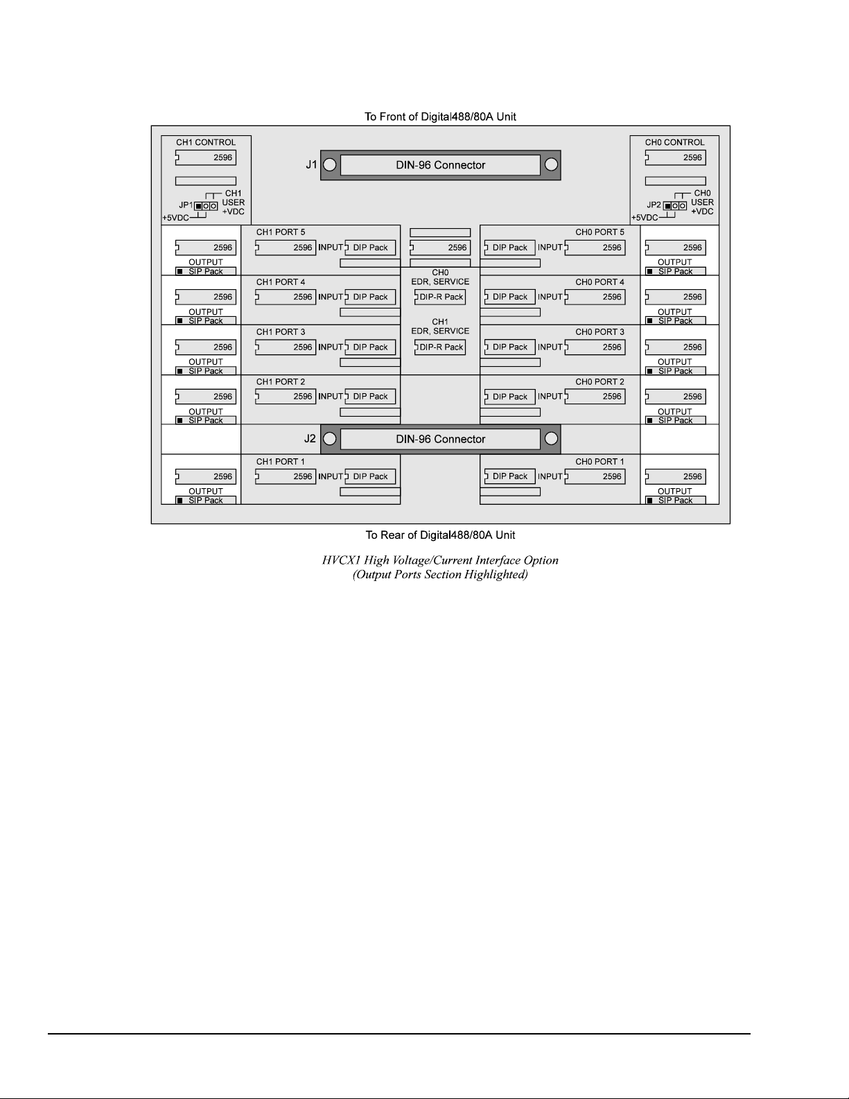
HVCX1 High Voltage/Current Interface Option
The HVCX1 option permits the I/O lines to be configured as high voltage (up to 50 V) inputs or as high
voltage/high current outputs (up to 200 mA sink capability) to allow interfacing with solenoids, switching
relays and other high voltage/high current devices using an external voltage source. It allows interfacing to
non-TTL level devices by offering compatibility with 12, 24 and 48 volt logic. The individual 8-bit ports
can be configured to control high current open collector drivers. Each high current driver has an internal
fly-back diode for protection when switching inductive devices such as relays. When the HVCX1 option is
used, the six handshake and control lines can also interface to 12, 24, or 48 volt logic.
Power-Up & Setup Configuration
The Digital488/80A allows up to 100 configurations for each channel to be created. The configurations are
stored in non-volatile memory, which enables the input/output status and logic level of every I/O line to be
defined when power is applied. The configurations can be called from a single pre-defined command from
the IEEE 488 controller. This allows easy configuration of the device for a variety of applications.
Internal pull-up resistors ensure a logic "high" the instant power is applied. When using the HVCX1
option with high current driver outputs, the internal pull-up resistors ensure that the high current driver
outputs are switched off the instant power is applied -- a requirement for process control applications.
Internal Buffer
A built-in data buffer in the Digital488/80A can store up to 8,000 bytes, which is large enough to capture
two thousand patterns from one 40-bit I/O channel. When interfacing to slow devices, the data buffer
relieves the controller of the need to constantly read data from the Digital488/80A.
Software Programmable Features
The software programmable features on the Digital488/80A include data formats, individual bit set and bit
clear commands and terminators. The six available data formats are ASCII hexadecimal, ASCII character,
ASCII binary, binary, high speed binary and ASCII decimal. The programmable terminators facilitate
interfacing to various controllers. Using the User Status (
programmed status of the Digital488/80A at any time. With the Query (
Digital488/80A command, user-defined status command strings can be built to request the status
information needed for a given application.
Accessories
Additional accessories that can be ordered for the Digital488/80A include:
• CA-1: Power cable
• CA-7-1: 1.5-foot IEEE 488 cable
• CA-7-3: 6-foot shielded IEEE 488 cable
• CA-7-4: 6-foot reverse entry IEEE 488 cable
• CA-88: 6-foot 50-pin D-shell ribbon cable
• CN-20: Right-angle IEEE 488 adapter, male and female
• CN-22: IEEE 488 multi-tap bus strip, four female connectors in parallel
• CN-23: IEEE 488 panel-mount feed-through connector, male and female
U) command, the controller can check the
?) option offered with each
2 Digital488/80A Overview 11-07-02 Digital488/80A User's Manual
Page 9
Specifications
Digital I/O
Terminal Installation Category: Standard: Not Applicable. CE: Category 1.
Digital I/O Capability: Dual Channels, each with five 8-bit ports, programmable as inputs or outputs.
Also included per channel are programmable handshake lines, data latching cap ability, a Service
Request (SRQ) input and Clear and Trigger outputs.
Logic Levels: Outputs drive 2 TTL loads (3.2 mA). Optional 12, 24, 48 volt logic support available with
the HVCX1 High Voltage/Current Interface option.
High-Current Outputs: With the HVCX1 option, the outputs can be configured, in groups of eight, as
high current outputs. Each high-current output is capable of sinking up to 200 mA at 50 VDC
maximum. Total current sinking capability is 8 A maximum.
Update Rate: In binary mode, the Digital488/80A can update one 40-bit I/O channel at over 2 Kbytes per
second.
I/O Port Connections: Two 50-pin male D-shell connectors. Mating solder tab connectors are supplied.
Input Ranges, Nominal Logic Low/High Voltages (±10%), and Input Resistances (HVCX1 option
only):
0-5 Volt Range: 0.8 volts low / 2.4 volts high; 15 Kohms.
0-12 Volt Range: 1.9 volts low / 5.75 volts high; 35 Kohms.
0-24 Volt Range: 4.2 volts low / 11.5 volts high; 61 Kohms.
0-48 Volt Range: 8.4 volts low / 23 volts high; 135 Kohms.
Please read this manual carefully! If equipment is used in any manner not specified in
this manual, the protection provided by the equipment may be impaired.
CAUTION
IEEE 488
General
The IEEE 488 terminal must only be used to control a non-isolated IEEE 488 system.
The common mode voltage (cable shell to earth) must be zero.
Terminal Installation Category: Standard: Not Applicable. CE: Category 1.
Implementation: SH1, AH1, T4, TE8, L4, LE4, SR1, RL0, PP0, DC1, DT1, C0, E1.
Terminators: Ignored on input. Selectable CR, LF, LF-CR or CR-LF, with or without EOI.
Programmable: IEEE Bus Terminators, EOI Control, SRQ Mask, Port Data, Active Levels, Handshake
Lines, Format, and Configuration.
Connector: Standard IEEE 488 connector with metric studs.
WARNING
Service: Fuse replacement and the changing of selected line voltage must be
performed by qualified service personnel. Never open the case while it is connected to
the AC line. Internal voltage potentials exist which could cause bodily injury or death.
CAUTION
Digital488/80A User’s Manual Digital488/80A Overview 3
Page 10
Terminal Installation Category: Standard: Not Applicable. CE: Category 2 for Line Voltage Input
terminal. All other terminals are Category 1.
Dimensions: 425 mm wide x 45 mm high x 203 mm deep (16.75" x 1.75" x 8").
Weight: 2 kg. (4.5 lbs).
Environment: Standard: Indoor use, 0° to 50°C; 0 to 95% RH (non-condensing).
CE: Indoor use at altitudes below 2000 meters, 0° to 40°C; 0 to 80% RH up to 31°C decreasing
linearly 4% RH/°C to 40°C.
Controls: Power switch (external), line voltage selection switch (internal), and DIP switch (external) for
IEEE 488 addressing mode and IEEE 488 address.
Indicators: LED indicators for TALK, LISTEN, SRQ, ERROR, TEST and POWER.
Power: Internally selectable 105-125 or 210-250 VAC; 50/60 Hz, 30 VA maximum.
Fuse: 1/2A Slo Blo 3AG (for 105-125 V power line) or 1/4A Slo Blo 3AG (for 210-250 V power line).
CAUTION
Line Voltage: The protective conductor terminal on the AC line connector must be
connected to an external protective earthing system. Failure to make such a
connection will impair protection from shock.
CAUTION
Fuse Failure: Fuse failure indicates a possible problem within the device circuitry. If a
fuse blows, contact a qualified service representative. Replacement fuses are to be
installed by qualified service personnel with the unit disconnected from the power
source and with all other terminals disconnected. If the line voltage selector is
changed, then the fuse designated for that line voltage must be used.
Data Transfer Speeds
The Digital488/80A has been measured to perform at the approximate speeds listed below. The testing
was done in such a way that the limiting factor was the Digital488/80A and not the IEEE 488 bus
controller driving it. All explanations discuss only one channel although the specifications given are valid
for either channel.
• Collection and Storage of Data: The Digital488/80A has an internal data buffer capable of storing
2000 readings of 40-bit data per channel. When operating in the
buffered on an External Data Ready transition), a transition on the EDR input causes the
Digital488/80A to collect the current value of all 40 bits and store the reading in the buffer. This
collection and storage of 40 bits of data can occur at a maximum rate of once every 140 microseconds.
• Output of Data to Ports: When sending data to the outputs on a Digital488/80A channel, the fastest
format mode is high-speed binary mode: Format (
data are accepted from the bus and sent directly to the Digital488/80A outputs (all 40 bits). This
constitutes one data transfer. The data transfer rate in this mode is approximately 1400 transfers per
second.
• IEEE 488 Bus Communication: The fastest data transfer rate across the IEEE 488 bus to the
IEEE 488 controller is approximately 1 byte every 140 microseconds whether reading data from the
internal data buffer, or accepting commands or data from the bus.
• Transistor-Transistor Logic (TTL) Levels: The data and handshake output lines drive two TTL loads.
In addition, Ports 1 and 2 on each channel can function as 5-volt CMOS-compatible outputs. All input
lines are less than 1.5 TTL loads. Normal precautions should be taken to limit the input voltages to the
range of -0.3 to +7.0 volts. All I/O lines are referenced to I/O Common (Ground; DB-50 Pin 50).
R2 mode (data are latched and
F) command F5. In this mode, 5 bytes of binary
4 Digital488/80A Overview 11-07-02 Digital488/80A User's Manual
Page 11

Digital488/80A Setup 2
The Package…… 5
Hardware Setup…… 6
Front & Rear Panel Layouts…… 6
Default DIP Switch Settings…… 7
IEEE 488 Bus Address Selection…… 7
Addressing Mode Selection…… 7
Dual Primary Addressing Mode…… 8
Secondary Addressing Mode…… 8
HVCX1 Option Setup…… 10
Determining Ports Setup…… 11
To Set Up Input Ports…… 12
To Set Up Handshaking Input Lines…… 13
To Set Up Output Ports…… 14
To Set Up Handshaking Output Lines…… 14
To Install the HVCX1 Option…… 16
Digital I/O Ports…… 17
Using the HVCX1 Option for High Voltage/Current Options…… 18
The Package
All Digital488/80A components are carefully inspected prior to shipment. When you receive your IEEE
488 / digital I/O interface, carefully unpack all items from the shipping carton and check for any damage
which may have occurred during shipment. Promptly report the damage to the shipping agent and your
sales representative. Retain all shipping materials in case you must return the unit to the factory.
Every Digital488/80A package includes the following items listed by part number:
• Digital488/80A: 80-Bit IEEE 488 / Digital I/O Interface
• 196-0901: Digital488/80A User’s Manual
• PR-2: Warranty Card
• 196-0800: Accessories Kit for Digital488/80A, which includes the following:
• CA-1: Power Cable
• HA-41-6: Rack Screws (4)
• FE-1: Rubber Feet (4)
• EN-6: Rack Ears (2)
• FU-1-.25: 1/4A Replacement Fuse
• FU-1-.5: 1/2A Replacement Fuse
• CN-18-50: Mating Connector for DB-50 (2)
In addition, if the High Voltage/Current Interface Option (HVCX1) is included, you will have the
following items:
• 196-4050: PCB Sub-Assembly, which includes a HVCX1 High Voltage/Current Interface
• 196-0801: Accessories Kit, HVCX1 Option for Digital488/80A, which includes the following:
• RN-3-20K: 20 Kohms Resistor, 16-pin DIP Pack (12)
• RN-3-56K: 56 Kohms Resistor, 16-pin DIP Pack (12)
• RN-3-120K: 120 Kohms Resistor, 16-pin DIP Pack (12)
• RN-9-27K: 27 Kohms Pullup Resistor, 9-pin SIP Pack (10)
Digital488/80A User’s Manual 11-08-02 Digital488/80A Setup 5
Page 12
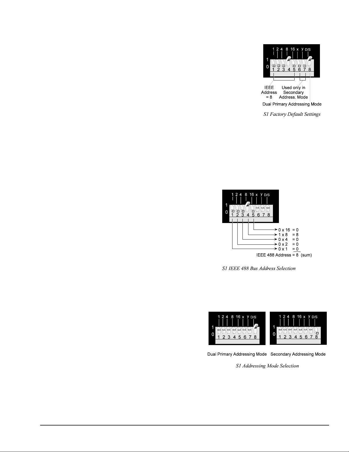
Hardware Setup
Do not use the Digital488/80A unit outdoors! This unit is intended for indoor use only!
Unexpected outdoor conditions could result in equipment failure, bodily injury or
death!
Front & Rear Panel Layouts
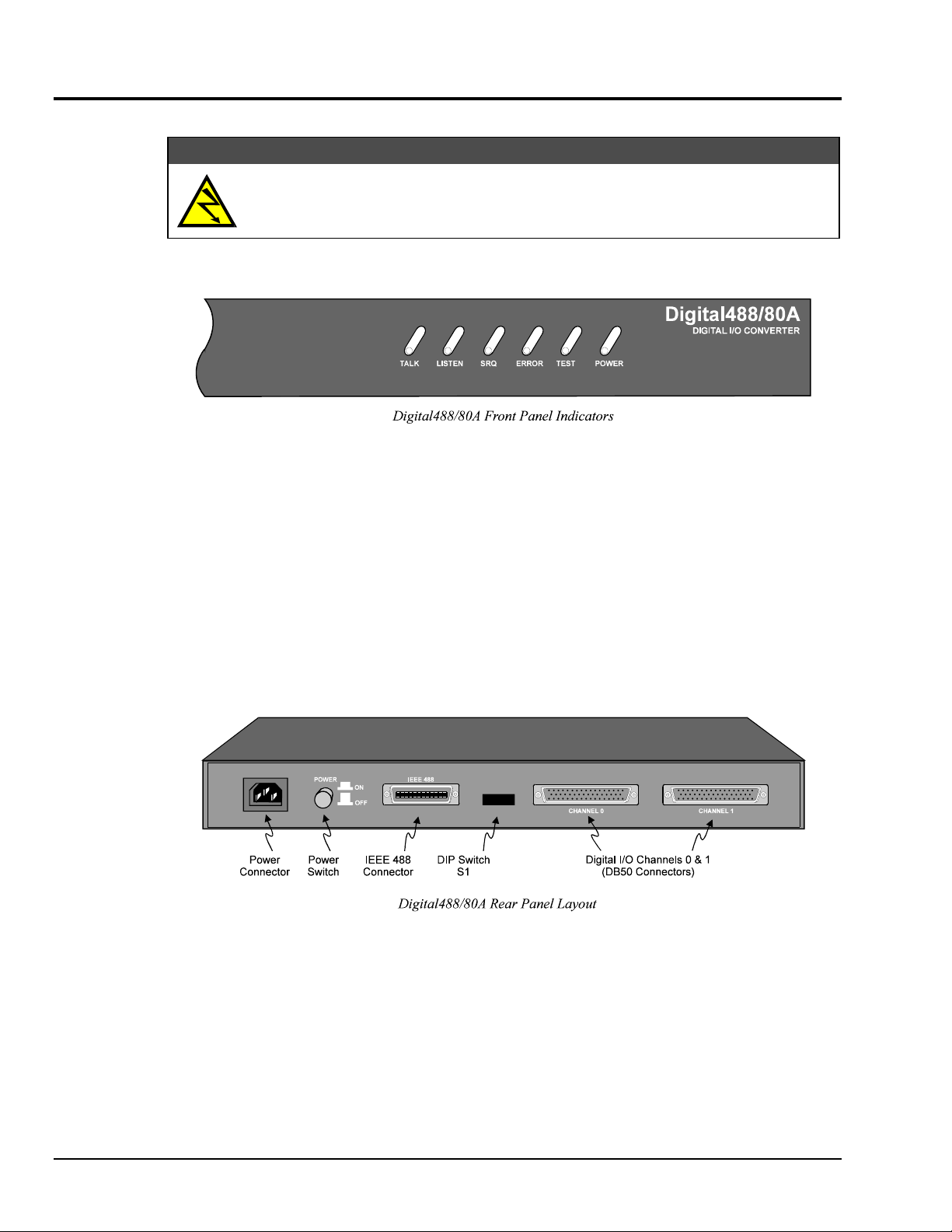
Six LED indicators on the Digital488/80A front panel, display the unit status. The following list describes
the functions of these indicators:
• TALK: ON when Digital488/80A is in the Talker state; OFF when in the Idle or Listener state.
• LISTEN: ON when Digital488/80A is in the Listener state; OFF when in the Idle or Talker state.
• SRQ: ON when Digital488/80A generated a service request; OFF when no SRQ is pending.
• ERROR: ON when an error has occurred; OFF when no error condition exists.
WARNING
• TEST: ON when used in conjunction with the Test (
T) command to verify that communication has
been established with the Digital488/80A.
• POWER: ON when power is being applied while the power switch is in the ON position; OFF when
power is not present.
6 Digital488/80A Setup Digital488/80A User's Manual
Page 13
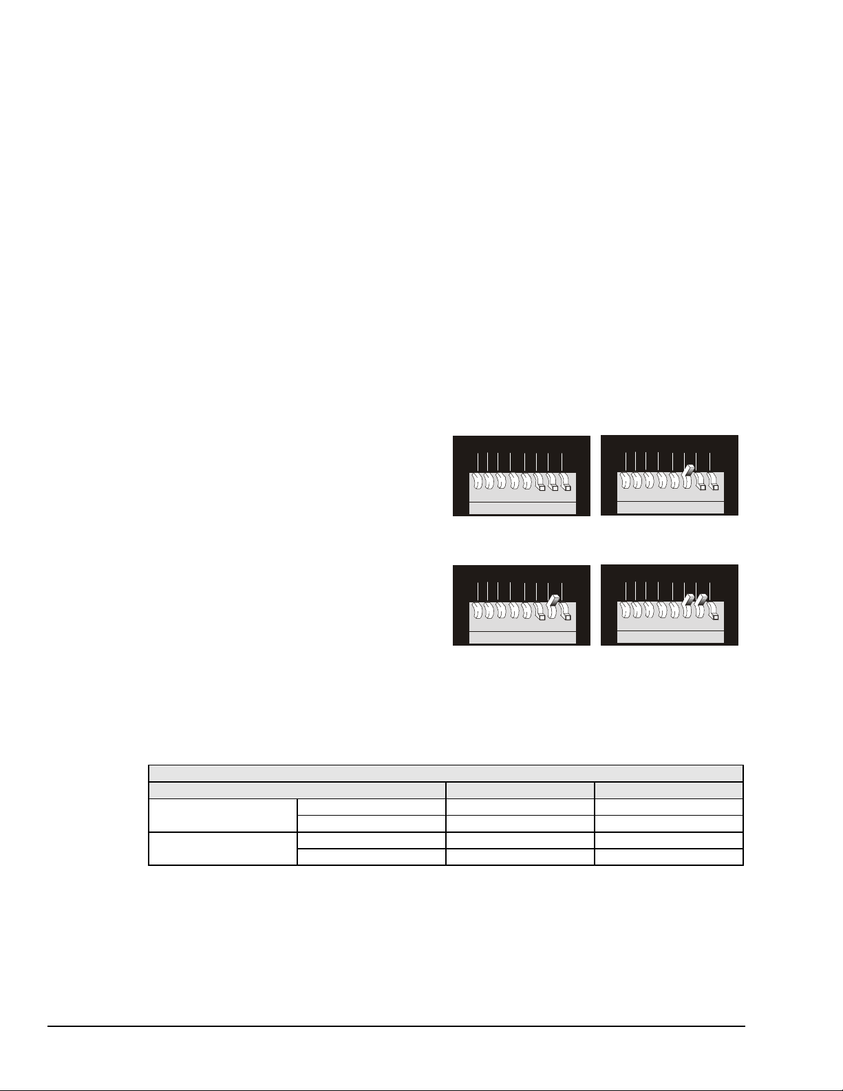
Default DIP Switch Settings
The Digital488/80A unit may be operated from either 110 VAC or 220
VAC. The operating voltage is set by an internal switch. The factory
set operating voltage appears on the label placed over the power jack on
the rear panel. To change the operating voltage, see section Line
Voltage Selection in Chapter 3: Digital488/80A Power & Assembly.
The Digital488/80A unit has one 8-microswitch DIP switch (S1)
accessible from the rear panel. This DIP switch determines the IEEE
488 bus address and its addressing mode. The switch is read only when
the unit is powered on and should be set prior to applying power. The
figure illustrates the factory default for the DIP microswitch settings:
IEEE 488 bus address = 8, and Addressing Mode = Dual Primary. In
the Dual Primary addressing mode, DIP microswitches 6 and 7 are
ignored.
Note: DIP switch S1 is read only during power up. For this reason you must make any setting changes
prior to applying power to the unit.
To modify the default settings, disconnect the power cord from the AC line and change the microswitch
settings using a small screwdriver. The enclosure does not need to be opened to change the DIP
microswitch settings.
IEEE 488 Bus Address Selection
The IEEE 488 bus address is set by positioning the
rear-panel DIP microswitches 1 through 5. The
address can be set from 0 through 30 and is read
only at power on. The address is selected by
simple binary weighting with microswitch 1 being
the Least Significant Bit (LSB; with a value of 1)
and microswitch 5 the Most Significant Bit (MSB;
with a value of 16). The factory default setting is
address 8, as shown in the diagram.
Note: If address 31 is selected, it defaults to
address 30 because the IEEE 488
standard has reserved address 31.
Note: The Digital488/80A bus address must
agree with the IEEE 488 controller
address.
Addressing Mode Selection
The Digital488/80A can be operated in one of two
addressing modes: Dual Primary addressing mode
or Secondary addressing mode, which are selected
by the rear-panel DIP microswitch 8. The factory
default setting for microswitch 8 is Dual Primary
addressing mode, in the "up" position as shown in
the diagram. A detailed description of the Dual
Primary and Secondary addressing modes is
provided in the following text.
Digital488/80A User’s Manual 11-08-02 Digital488/80A Setup 7
Page 14
Dual Primary Addressing Mode
The Digital488/80A can be thought of as two identical IEEE 488-to-digital I/O interfaces. Each interface
occupies one bus address and has one I/O channel. For this reason the Digital488/80A occupies two bus
addresses in an IEEE 488 system.
The default addressing mode on the Digital488/80A is "Dual Primary,” in which two consecutive bus
addresses are used. Dual Primary addressing offers ease of use at the expense of two bus address
locations. This may not be practical for applications in which the bus address locations are required by
other equipment. In these situations, “Secondary" addressing mode may be used. Secondary addressing
uses a single bus address for multiple interfaces.
When Dual Primary addressing mode is selected with DIP microswitch 8 in the "up" position, then
microswitch 1 (LSB of the address) is ignored. The Channel 0 interface resides at an even numbered bus
address, while the Channel 1 interface resides at the next higher odd address. For example, if the address
switches are set for IEEE 488 bus address 8, Channel 0’s interface resides at bus address 8 and Channel 1’s
interface resides at bus address 9.
Note: Because the IEEE 488 standard has reserved address 31, if address 30 is selected when in Dual
Primary addressing mode, then the Digital488/80A defaults to address 28 for Channel 0, and to
address 29 for Channel 1.
Secondary Addressing Mode
When Secondary addressing mode is selected with
DIP microswitch 8 in the "down" position, then up
to four Digital488/80A units can reside at the same
primary bus addresses. The Secondary addresses
at which Channel 0 and Channel 1 reside, are
selected with microswitches 6 and 7, as indicated
in the adjacent figure.
Note: When in the Secondary address mode, if
IEEE 488 primary address 31 is selected,
the Digital488/80A unit will
automatically default to primary address
30.
For example, if two Digital488/80A units are
configured for primary address 08, with the first
unit being configured for Secondary addresses 0
and 1, and the second unit configured for
Secondary addresses 2 and 3, then the
communication is as indicated by the following
table.
Communication Example
To Communicate With: Use Primary Address: Use Secondary Address:
Unit 1 Channel 0 08 00
Channel 1 08 01
Unit 2 Channel 0 08 02
Channel 1 08 03
2
1
8
4
1
0
1
0
N/A
N/A
N/A
N/A
2 3
1
4
Addresses 0 and 1
2
1
8
4
N/A
N/A
N/A
N/A
2 3
1
4
Addresses 4 and 5
16
5
16
5
N/A
N/A
y
x
6 7 8
y
x
6 7 8
D/S
D/S
2
1
1
N/A
N/A
0
2 3
1
Addresses 2 and 3
2
1
1
N/A
N/A
0
2 3
1
Addresses 6 and 7
Secondary Address Settings
4
N/A
N/A
4
4
8
N/A
N/A
4
5
16
5
N/A
N/A
6 7 8
y
x
6 7 8
D/S
D/S
y
8
16
x
8 Digital488/80A Setup Digital488/80A User's Manual
Page 15
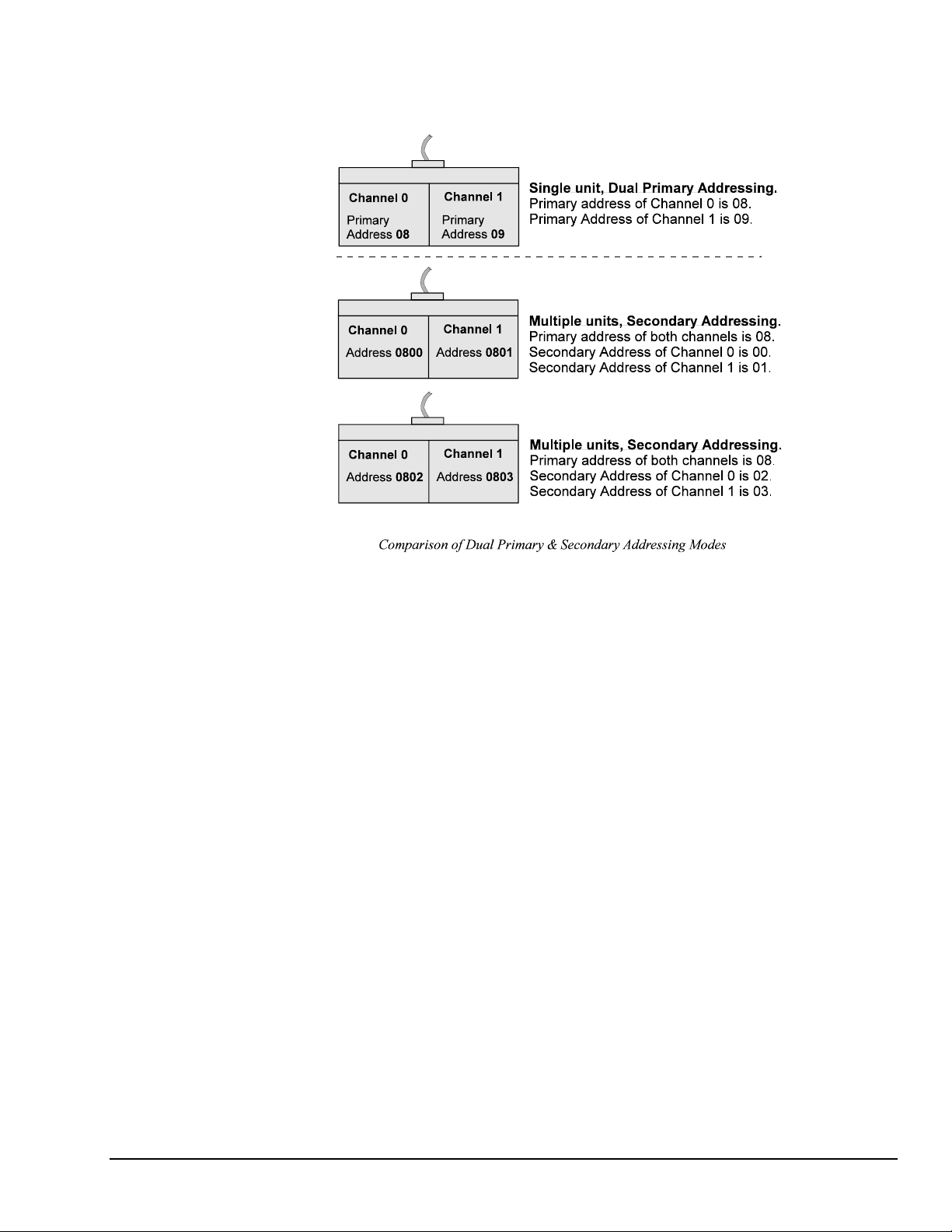
The following figure compares the Dual Primary and the Secondary addressing modes.
Digital488/80A User’s Manual 11-08-02 Digital488/80A Setup 9
Page 16
HVCX1 Option Setup
If you would like to experiment with the Digital488/80A unit and the example
programs, do not install the HVCX1 option until after experimenting with the unit to
avoid software/hardware configuration conflicts. If the HVCX1 option is already
installed, replace it with the jumper board to run the example programs.
Never disassemble the Digital488/80A case while it is connected to the AC power line!
Internal voltage potentials exist which could cause bodily injury or death!
The HVCX1 High Voltage/Current
Interface option is a configurable daughter
board that allows the Digital488/80A to be
used with solenoids, switching relays and
other high voltage / high current devices.
When using the HVCX1 with an exte
rnal
voltage source, the I/O lines may be
configured as high voltage inputs (up to 50
V) or as high voltage / high current ou
tputs.
The factory default is all 5 V I/O and
handshaking f
or both channels with all ports
set as inputs.
Inputs are configured on a port-by-port
basis (in groups of 8 bits). Inputs can be
configured to be compatible with 5, 12, 24
and 48 volt logic. The interface voltage fo
each port ma
y be set independently from
other ports.
CAUTION
WARNING
r
When the HVCX1 option is used, the data
lines of both channels can be configured as
high voltage / high current outputs. Outputs
can support up to 50 VDC at 200 mA no
t to
exceed 8 A total. When the outputs are
configured as high voltage, using internal
pull-up resistors (such as the 27K ohm SIP
),
all 40 output lines on a channel have their
pull-ups and integral flyback diodes pulled
up to the flyback pin (Pin 48) on the DB-50
connector. When used in this mode, outputs
are configured on a per-channel basis. T
his
flyback pin should be connected to the
positive supply lead of the power supply
used with the external devices. The flyback
diode suppl
ies protection against inductive
transients.
Pin 48 sets the pull-up logic level for all output lines on a channel. Lines configured with the pull-up can
only be used as outputs. These outputs can sink up to 200 mA in the ON state and withstand voltages up to
50 VDC throu
gh the use of open collector drivers with integral flyback diodes for inductive load transient
suppression.
For more information, see the "Specifications" section in Chapter 1: Digital488/80A Overview.
10 Digital488/80A Setup Digital488/80A User's Manual
Page 17
Determining Ports Setup
Before configuring the HVCX1 option, determine which ports are going to be set up for inputs and which
ports for outputs. Determine what voltages are desired for the inputs: 0-5 V, 0-12 V, 0-24 V or 0-48 V.
The following chart shows which combinations of outputs and inputs are permitted (limitations set by the
Configuration (
Configuration Command Port 5 Port 4 Port 3 Port 2 Port 1
C) software command).
C0
C1
C2
C3
C4
C5
Input Input Input Input Input
Input Input Input Input Output
Input Input Input Output Output
Input Input Output Output Output
Input Output Output Output Output
Output Output Output Output Output
Note: If no chips are installed in the input or output side of a port, the Digital488/80A lines are
pulled up and the user will receive "FF" from that port.
For convenience, you may want to program the Digital488/80A to power up with your configuration.
Refer to the Configuration (
the Configuration (
C) command. To save the input/output status as the new setting for the power-up
default, it must be saved as part of the Recall Configuration (
configuration upon power on, the Save Configuration (
C) and Save Configuration (S) commands. Input or output status is set using
O) command. To set the unit to a particular
S) command must be used once all the desired
options have been selected.
Digital488/80A User’s Manual 11-08-02 Digital488/80A Setup 11
Page 18
To Set Up Input Ports
Note: All of the components mentioned below are for the port section of the HVCX1 board
labelled INPUT.
1. Locate the two 5-port sections (one in the right half, one in the left half) of the HVCX1 board labelled
INPUT.
2. Place the 2596 IC chip into the IC input socket of the port being configured. The notched end of the IC
must be to the left (see above figure for the proper orientation).
3. Install the DIP (dual in-line) pack for the voltage desired. See the chart below for the DIP pack
labeling. The notched end of the DIP pack must be to the left (see above figure for the proper
orientation).
0-5 V 10 ohms 4116R-001-100
0-12 V 20K ohms 4116R-001-203
0-24 V 56K ohms 4116R-001-563
0-48 V 120K ohms 4116R-001-124
Inputs DIP Resistor Values Label of DIP Pack Supplied with HVCX1 Option
4. Verify that no components (the 2596 and SIP pack) are in the OUTPUT section of a port being
configured as an input. Having components for the output and input installed in the same port will
cause damage to the unit.
12 Digital488/80A Setup Digital488/80A User's Manual
Page 19
To Set Up Handshaking Input Lines
Note: All of the components mentioned below are for the central section of the HVCX1 board
labelled EDR, SERVICE.
1. Locate the center of the HVCX1 board labelled CH0 EDR, SERVICE and CH1 EDR, SERVICE.
2. Install the DIP (dual in-line) pack for the input handshaking voltage desired. See the chart below for
the DIP pack labeling. The notched end of the DIP pack must be to the left (see above figure for the
proper orientation).
0-5 V 10 ohms 4116R-001-100
0-12 V 20K ohms 4116R-001-203
0-24 V 56K ohms 4116R-001-563
0-48 V 120K ohms 4116R-001-124
Inputs DIP Resistor Values Label of DIP Pack Supplied with HVCX1 Option
3. Verify that the appropriate DIP packs are installed in the CH0 EDR, SERVICE section fo r the Channel
0 settings, and in the CH1 EDR, SERVICE section for the Channel 1 settings.
Digital488/80A User’s Manual 11-08-02 Digital488/80A Setup 13
Page 20
To Set Up Output Ports
Note: All of the components mentioned below are for the port section of the HVCX1 board
labelled OUTPUT.
1. Locate the two 5-port sections (one in the right end, one in the left end) of the HVCX1 board labelled
OUTPUT.
2. Place the 2596 IC chip into the IC input socket of the port being configured. The notched end of the IC
must be to the left (see above figure for the proper orientation).
3. When configuring the option for high voltage, install the 27K SIP (single in-line) pack pull-up resistor
network (labeled 9X-1-273) in the SIP socket in the OUTPUT section. Make sure Pin 1 of the SIP
pack, as denoted by the square dot, is toward the left (see above figure for the proper orientation). This
pin must be connected to an external voltage supply in order to achieve the desired logic level.
4. Verify that no components (the 2596 and DIP pack) are in the INPUT section of a port being
configured as an output. Having components for the output and input installed in the same port will
cause damage to the unit.
To Set Up Handshaking Output Lines
With the HVCX1 option, the Digital488/80A handshaking outputs (Trigger, Inhibit, Strobe and Clear) can
be set. The user-defined voltage is the voltage supplied through Pin 48 of the channel (voltage is the same
as the data lines for ports configured as outputs). Handshaking output lines are changed as a group and
cannot have their sense reconfigured; handshaking inputs are always inputs, and handshaking outputs are
always outputs. There is one group of handshaking output lines per channel (i.e. CH0 has handshaking set
and CH1 has handshaking set). Handshaking may be done at TTL levels even if digital I/O is set for a
higher range.
14 Digital488/80A Setup Digital488/80A User's Manual
Page 21
Note: All of the components mentioned below are for the upper-corner sections of the HVCX1
board labelled CONTROL.
1. Locate the upper corners of the HVCX1 board labelled CH1 CONTROL and CH0 CONTROL.
2. In these CH1 CONTROL and CH0 CONTROL sections, the handshaking outputs are set by jumpers
JP1 and JP2, for either +5 VDC (TTL) or a user-defined voltage (see following figure for the proper
jumper settings).
Digital488/80A User’s Manual 11-08-02 Digital488/80A Setup 15
Page 22
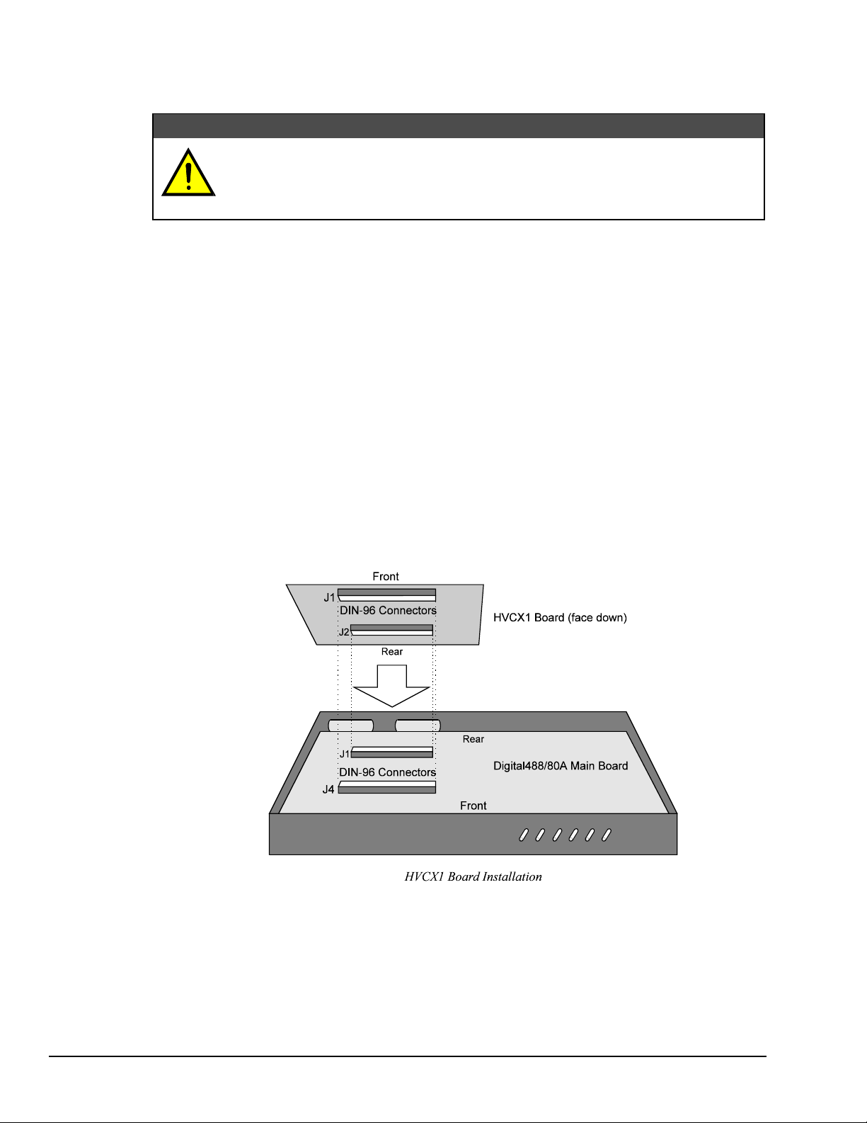
To Install the HVCX1 Option
Note: If disassembly or disconnections are necessary, first turn off the power, next disconnect the AC
1. When the input and output port configurations on the HVCX1 option are complete, record the settings
on the Digital488/80A HVCX1 Configuration Record supplied with your user's manual or provided in
Appendix A of this manual.
2. Turn off the power. Next, disconnect the AC power line cord, and then all other test cables from the
unit.
3. Place the unit on a flat surface. Remove the four screws on top of the case and remove the top cover.
4. Locate the two DIN-96 connectors on the HVCX1 board labelled J1 and J2, and the two DIN-96
connectors on the Digital488/80A main board labelled J4 and J1.
Note: If the HVCX1 option was not factory installed, the DIN-96 connectors have a jumper board
5. Hold the HVCX1 board upside down, with the label FRONT toward the front of the Digital488/80A
and the label REAR toward the back of the Digital488/80A.
6. Line up the J1 DIN-96 on the HVCX1 board with the J4 DIN-96 on the Digital488/80A main board.
Line up the J2 DIN-96 on the HVCX1 board with the J1 DIN-96 on the Digital488/80A main board.
When the HVCX1 option is used, the I/O lines are hardware configured as either
inputs or outputs. The hardware and software configurations for the input and output
ports must agree. The Digital488/80A unit is protected from configuration conflict,
but the I/O lines will not respond properly.
power line, and then any other cables, prior to disassembly.
plugged into them. Remove the jumper board.
CAUTION
7. Press down the HVCX1 board gently but firmly to plug together the DIN-96 connectors. Be careful not
to bend any DIN-96 connector pins.
8. Carefully reassemble the unit.
Note: For re-assembly, first reconnect the AC power line, and then any other cables, prior to reapplying
power to the entire system.
16 Digital488/80A Setup Digital488/80A User's Manual
Page 23
Digital I/O Ports
CAUTION
When the HVCX1 option is used, the I/O lines are hardware configured as either
inputs or outputs. The hardware and software configurations for the input and output
ports must agree. The Digital488/80A unit is protected from configuration conflict,
but the I/O lines will not respond properly.
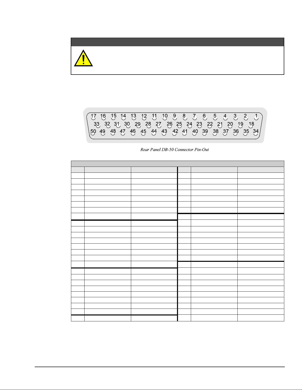
The Digital488/80A has two DB-50 connectors -- Channel 0 and Channel 1 -- each of which provides 40
data lines programmable in groups of 8 bits as either input or output ports. The following figure illustrates
one of the digital I/O DB-50 connectors as viewed from the rear panel of the Digital488/80A. Both
Channel 0 and Channel 1 DB-50 connectors are identical.
DB-50 Con or nect
Pin Description Comment Pin Description Comment
1 Port 1 Bit 1 I/O, Port 1 LSB 26 Port 4 Bit 2 Input/Output
2 Port 1 Bit 2 Input/Output 27 Port 4 Bit 3 Input/Output
3 Port 1 Bit 3 Input/Output 28 Port 4 Bit 4 Input/Output
4 Port 1 Bit 4 Input/Output 29 Port 4 Bit 5 Input/Output
5 Port 1 Bit 5 Input/Output 30 Port 4 Bit 6 Input/Output
6 Port 1 Bit 6 Input/Output 31 Port 4 Bit 7 Input/Output
7 Port 1 Bit 7 Input/Output 32 Port 4 Bit 8 I/O, Port 4 MSB
8 Port 1 Bit 8 I/O, Port 1 MSB 33 Port 5 Bit 1 I/O, Port 5 LSB
9 Port 2 Bit 1 I/O, Port 2 LSB 34 Port 5 Bit 2 Input/Output
10 Port 2 Bit 2 Input/Output 35 Port 5 Bit 3 Input/Output
11 Port 2 Bit 3 Input/Output 36 Port 5 Bit 4 Input/Output
12 Port 2 Bit 4 Input/Output 37 Port 5 Bit 5 Input/Output
13 Port 2 Bit 5 Input/Output 38 Port 5 Bit 6 Input/Output
14 Port 2 Bit 6 Input/Output 39 Port 5 Bit 7 Input/Output
15 Port 2 Bit 7 Input/Output 40 Port 5 Bit 8 I/O, Port 5 MSB
16 Port 2 Bit 8 I/O, Port 2 MSB 41 Clear Output only
17 Port 3 Bit 1 I/O, Port 3 LSB 42 Data Strobe Output only
18 Port 3 Bit 2 Input/Output 43 Trigger Output only
19 Port 3 Bit 3 Input/Output 44 Inhibit Output only
20 Port 3 Bit 4 Input/Output 45 Service Input Input only
21 Port 3 Bit 5 Input/Output 46 External Data Ready Input only
22 Port 3 Bit 6 Input/Output 47 (Not Used) (Not Used)
23 Port 3 Bit 7 Input/Output 48 HVCX1 Flyback Flyback
24 Port 3 Bit 8 I/O, Port 3 MSB 49 +5 V 50 mA maximum load
25 Port 4 Bit 1 I/O, Port 4 LSB 50 I/O Common Ground
Digital488/80A User’s Manual 11-08-02 Digital488/80A Setup 17
Page 24
Using the HVCX1 Option for High Voltage/Current Outputs
The HVCX1 option provides buffering for all the digital I/O lines on the Digital488/80A. This means that
the HVCX1 option has 80 digital I/O lines that are divided into two 40-bit channels -- Channel 0 and
Channel 1. Each channel is divided into five eight-bit ports. Six high-level ASCII commands configure
the ports to be all inputs, all outputs or combinations in between. Thus, a configuration can range from 80
input lines to 80 output lines or combinations in between in multiples of 8 bits.
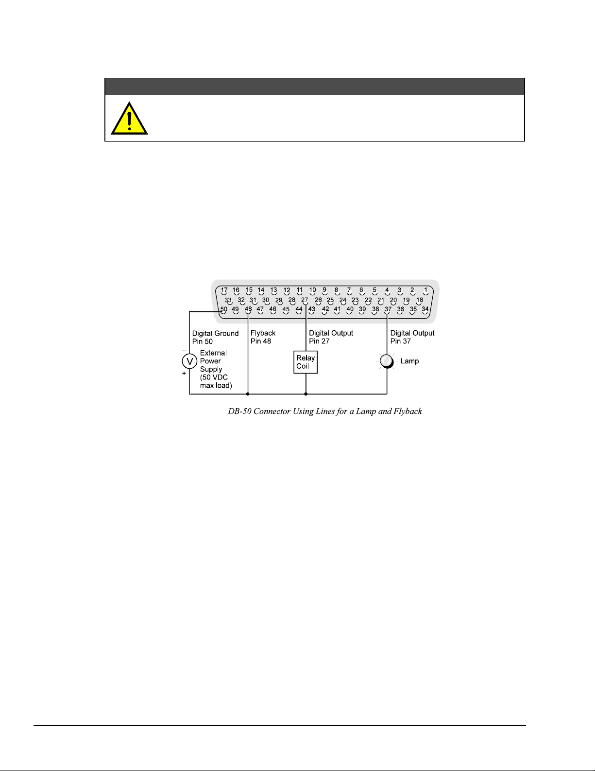
Once the Channel port(s) are configured for high level operation, they can be used to drive devices such as
switching relays, solenoids and displays. For example, a typical application may require a lamp and a relay
to be driven by the Digital488/80A. The relay is connected to data line 27 (Port 4) and the lamp is
connected to data line 37 (Port 5). These two ports must be configured as high-level outputs. These
devices would be connected as shown in the following figure.
Never connect external high-level devices to a Channel 0 port or to a Channel 1 port
which has not first been configured for this purpose. Failure to do so may result in
damage to the Digital488/80A.
CAUTION
Since a relay is used for this application, the flyback terminal is connected to the positive terminal of the
external power supply. Note also that the Ground lead of the power supply should be connected to Pin 50
on the DB-50 connector. Remember that ports configured as high-level outputs can only be used as
outputs.
18 Digital488/80A Setup Digital488/80A User's Manual
Page 25
Digital488/80A Power & Assembly 3
Introduction…… 19
Internal Components…… 19
Factory Service…… 19
Power Line & Fuse Configuration…… 20
Line Voltage Selection…… 20
To Select the Line Voltage…… 21
Fuse Replacement…… 22
To Replace the Fuse…… 22
Rack-Mount & Bench-Top Assembly…… 23
Rack Mount…… 23
Bench Top…… 23
Power-Up & Programming Tests…… 24
Power-Up Activation…… 24
Programming Examples……25
KYBDCTRL.BAS Program…… 25
To Run the Keyboard Controller Program…… 25
Digital488/80A Command Responses…… 26
Introduction
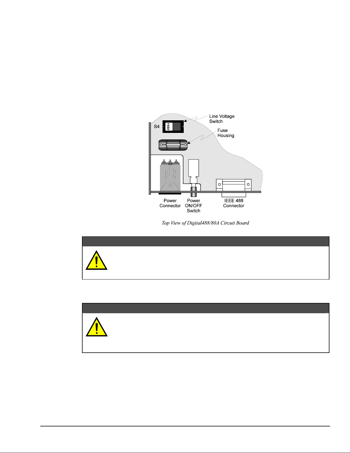
Internal Components
The heart of the Digital488/80A is a 6809 microprocessor [U1] supported by 8K bytes of firmware
EPROM [U2] and 32K bytes of battery-backed-up RAM [U3]. Interface to the IEEE 488 bus is
accomplished by a 9914 interface chip [U13]. A 65B22 [U14] generates real-time interrupts for the
firmware operating system and also drives the front panel LED indicators. The digital I/O ports are
controlled through 6821 interface chips [U7, U8, U9, U10, U11, U16]. High-voltage, high-current output
capability is provided on both channels if the HVCX1 option is used. Power is supplied by an on-board
transformer and full-wave rectifier. Regulation to the required +5 volts is provided by an 78T05CT [U15].
The memory space allocation on the Digital488/80A is:
Factory Service
Chapter 7: Troubleshooting provides a troubleshooting reference for possible solutions to technical
problems. Before calling for technical assistance, refer to this chapter.
However, if problems in using the Digital488/80A still persist, you should contact the factory. Many
problems can be resolved by discussing the problems with the appropriate applications department. If the
problem cannot be solved by this method, you will be instructed as to the proper return procedure.
Address Device Part Number Function
$0000-$7FFF U3 84256 32K x 8 RAM
$8010-$8014 U7 68B21 Digital I/O
$8020-$8024 U8 68B21 Digital I/O
$8040-$8044 U9 68B21 Digital I/O
$8080-$8084 U10 68B21 Digital I/O
$8100-$8104 U11 68B21 Digital I/O
$8200-$8204 U16 68B21 Digital I/O
$8800-$8810 U14 65B22 Timer, Digital I/O
$9000-$9907 U13 TMS9914A IEEE 488 Interface
$E000-$FFFF U2 2764 Programmed EPROM
Digital488/80A User’s Manual Digital488/80A Power & Assembly 19
Page 26
Power Line & Fuse Configuration
The power configuration of the Digital488/80A unit consists of selecting the line voltage and replacing the
fuses. Each Digital488/80A unit has a factory default to operate at 105-125 volts AC. However, each unit
may be operated at either 105-125 or 210-250 VAC.
To change the operating voltage of the Digital488/80A unit, it is necessary to open the enclosure.
However, before modifying the voltage, disconnect any input or output connections from the rear panel of
the affected unit and then disconnect the power cord from the power line terminal.
Line voltage must be set for 105-125 or 210-250 VAC to match the power being supplied to the
Digital488/80A unit. If the line voltage is changed
text for the line
Line Voltage Selection
As already mentioned, the Digital488/80A may be operated with 105-125 or 210-250 VAC, 50-60 Hz
power, as set by its internal line-voltage switch (labeled S4). Each unit is shipped from the factory with
this operating voltage setting marked on its rear panel. If this is not the appropriate power setting to be
supplied to the unit, then the line voltage and power fuse must be changed to avoid damage to the unit.
The line-voltage selection procedure is outlined in the following steps.
WARNING
Do not use the Digital488/80A unit outdoors! The unit is intended for indoor use only!
Outdoor conditions could result in equipment failure, bodily injury or death!
WARNING
Never disassemble the Digital488/80A case while it is connected to the AC power line!
Internal voltage potentials exist which could cause bodily injury or death!
, the fuse must also be changed. Refer to the following
voltage switch and fuse locations.
CAUTION
Service: Fuse replacement and the changing of selected line voltage must be
performed by qualified service personnel. Never open the Digital488/80A case while it
is connecte
or death!
d to the AC line. Contact with voltage potentials could cause bodily injury
20 Digital488/80A Power & Assembly Digital488/80A User's Manual
Page 27
Note: If disassembly or disconnection is necessary, first turn off the power, next disconnect the AC
power line, and then any other cables, prior to disassembly.
To Select the Line Voltage
1. Turn off the power. Next, disconnect the AC power line cord, and then all other test cables from the
unit.
2. Place the unit on a flat surface. Remove the four screws on top of the case and remove the top cover.
3. Located next to the main power supply transformer is the line voltage selection switch (labeled S4).
Using a small screwdriver, insert the tip of the screwdriver into the slot of the switch and slide the
switch to the left or right until it "clicks" into place with the desired line voltage selection visible.
CAUTION
It is possible to place the line voltage switch (S4
cause equipment damage or malfunction. Whe
V or 220 V selection. The switch will “click” into place when properly positioned.
voltage selection swi
tch (S4), make sure the switch is completely positioned to the 115
) in a partial position which could
n changing the position of the line
4. Install a power line fuse appropriate for the line voltage. See section Fuse Replacement – Step 3,
following this section.
CAUTION
Fuse Failure: Fuse failure indicates a possible problem within the device circuitry. If
a fuse blows, contact a qualified service representative. Replacement fuses are to be
installed by qualified service personnel with the unit disconnected from the power
source and with all other terminals disconnected. If the line voltage selector is
changed, then the fuse designated for that line voltage must be used.
5. Make note of the new voltage setting for later reference.
6. Carefully reassemble the unit.
Note: For re-assembly, first reconnect the AC power line, and then any other cables, prior to reapplying
power to the entire system.
Digital488/80A User’s Manual Digital488/80A Power & Assembly 21
Page 28
Fuse Replacement
The Digital488/80A unit contains an internal AC line fuse. The fuse is located next to the internal linevoltage switch (S4). You may replace the fuse by using the procedures found in the following text.
Note: If disassembly or disconnection is necessary, first turn off the power, next disconnect the AC
To Replace the Fuse
1. Turn off the power. Next, disconnect the AC power line cord, and then all other cables from the unit.
2. Place the unit on a flat surface. Remove the four screws on top of the case and remove the top cover.
3. Located next to the line-voltage selection switch (labeled S4) is the power fuse. Gently pull upward
on the plastic fuse housing. The entire housing with the fuse inside should be removed.
4. Open the fuse housing by pushing up on the tab on the bottom of the housing. Remove the fuse, and
replace it with the proper type using the following list as a guide:
• For line voltage 105-125 V, use fuse type 1/2 A, Slo Blo, 3AG
• For line voltage 210-250 V, use fuse type 1/4 A, Slo Blo, 3AG
Service: Fuse replacement and the changing of selected line voltage must be
performed by qualified service personnel. Never open the Digital488/80A case while it
is connected to the AC line. Contact with voltage potentials could cause bodily injury
or death!
power line, and then any other cables, prior to disassembly.
CAUTION
5. Close the housing. Insert the fuse into the fuse holder.
6. Make note of the new fuse rating for later reference. If you have also changed the operating line-
voltage selection, return to the previous section Line Voltage Selection – Step 5.
7. Carefully reassemble the unit.
Note: For re-assembly, first reconnect the AC power line, and then any other cables, prior to reapplying
Fuse Failure: Fuse failure indicates a possible problem within the device circuitry. If
a fuse blows, contact a qualified service representative. Replacement fuses are to be
installed by qualified service personnel with the unit disconnected from the power
source and with all other terminals disconnected. If the line voltage selector is
changed, then the fuse designated for that line voltage must be used.
power to the entire system.
CAUTION
22 Digital488/80A Power & Assembly Digital488/80A User's Manual
Page 29
Rack-Mount & Bench-Top Assembly
The Digital488/80A includes accessories for rack-mount or bench-top assembly.
Rack Mount
If rack-mount assembly is required, remove the two plastic screws from the pre-drilled holes on each side
of the unit. Since the unit can be mounted with the front or rear panel facing the front of the rack fixture,
remove only those screws from the set of holes that will be toward the front of the rack. Attach the two
rack ears using the enclosed screws.
Bench Top
If bench-top assembly is required, install the self-adhesive rubber feet on the bottom of the unit
approximately one inch from each corner.
Digital488/80A User’s Manual Digital488/80A Power & Assembly 23
Page 30
Power-Up & Programming Tests
Power-Up Activation
Condition
Normal (No Errors)
ROM Error
RAM Error
NV-RAM Checksum Error
No Power
With the power cord plugged in and connected to the Digital488/80A, turn on the unit by depressing the
rear-panel power switch. All of the front-panel LED indicators should light up for approximately one
second while the Digital488/80A performs an internal ROM and RAM self-check. At the end of this selfcheck all of the LED indicators should turn off except for POWER.
Otherwise, the Digital488/80A may be in an error condition according to the one of the four following
LED patterns:
• If all of the LED indicators remain on: Then a ROM error has occurred.
• If the POWER LED indicator remains on while the rest of the LED indicators flash continuously:
Then a RAM error has occurred. Try cycling the power to the Digital488/80A to determine that the
error is repeatable.
Line Voltage: The protective conductor terminal on the AC line connector must be
connected to an external protective earthing system. Failure to make such a
connection will impair protection from shock.
LED Patterns for Error Conditions
LED Indicators
TALK LISTEN SRQ ERROR TEST POWER
(Off) (Off) (Off) (Off) (Off) ON
ON ON ON ON ON ON
FLASHING FLASHING FLASHING FLASHING FLASHING ON
(Off) (Off) (Off) ON (Off) ON
(Off) (Off) (Off) (Off) (Off) (Off)
CAUTION
• If the POWER and ERROR LED indicator remain on while the rest of the LED indicators are off:
Then a checksum error on Non-Volatile RAM occurred, and the saved configurations may be lost.
The checksum error condition may be cleared by doing a save of a configuration using the Save
Configuration (
S) command.
Note: The error condition cannot be cleared by using the Query Error Status (E?) command.
• If all of the LED indicators are off: Then there may not be any power being supplied to the
Digital488/80A. In this event, check to make sure that the AC power cable is securely connected at
both ends. Otherwise, there may be a problem with the fuse. For more information, see section Power
Line & Fuse Configuration earlier in this chapter.
For convenience, you may want to program the Digital488/80A to power up with your configuration.
Refer to the Configuration (
the Configuration (
C) command. To save the input/output status as the new setting for the power-up
default, it must be saved as part of the Recall Configuration (
configuration upon power on, the Save Configuration (
C) and Save Configuration (S) commands. Input or output status is set using
O) command. To set the unit to a particular
S) command must be used once all the desired
options have been selected.
24 Digital488/80A Power & Assembly Digital488/80A User's Manual
Page 31

Programming Examples
The Digital488/80A programming examples use the Personal488 PC/IEEE 488 controller interface and the
BASIC Keyboard Controller (KBC) program. This KBC program
and is listed below.
KYBDCTRL.BAS Program
10 ' Personal488 Keyboard Controller Program
20 '
30 ' For use with the IOtech Personal488
40 ' IEEE 488 interface
50 '
100 OPEN "\DEV\IEEEOUT" FOR OUTPUT AS #1
110 IOCTL#1,"BREAK"
120 PRINT#1,"RESET"
130 OPEN "\DEV\IEEEIN" FOR INPUT AS #2
140 '
150 ON ERROR GOTO 300
160 PRINT#1,"ERROR OFF"
170 '
180 LINE INPUT "CMD> ",CMD$
190 PRINT#1,CMD$
200 '
210 IF IOCTL$(2)<>"1" THEN 180
220 PRINT INPUT$(1,2);
230 GOTO 210
290 '
300 ' Error Handler
310 '
320 IOCTL#1,"BREAK"
330 PRINT#1,"STATUS"
340 INPUT#2,ST$
350 PRINT CHR$(7);"Error #";MID$(ST$,15,2);": ";MID$(ST$,27)
360 RESUME NEXT
KYBDCTRL.BAS is included on the disk
The Keyboard Controller (KBC) program allows direct communication with the Digital488/80A (or any
IEEE 488 device on the bus) via the keyboard, and displays any responses on the screen. This program is a
convenient method of exercising the Digital488/80A and becoming familiar with the commands and their
actions.
To Run the Keyboard Controller Program
CAUTION
This programming example will not work properly if the HVCX1 option is installed.
Remove the HVCX1 board and replace it with the jumper board to run this example.
1. First, verify that the rear-panel DIP switch S1 is set for Dual Primary addressing mode (factory
default), and for IEEE 488 bus primary address 8 (factory default).
2. Connect an IEEE 488 cable from the IEEE 488 connector on the Digital488/80A to the IEEE 488
connector on the Personal488 PC/IEEE 488 controller interface card.
3. Turn on the Digital488/80A by depressing the rear-panel power switch. All of the front-panel LED
indicators should light up for approximately one second while the Digital488/80A performs an internal
ROM and RAM self-check. At the end of this self-check all of the LED indicators should turn off
except for POWER.
4. From the MS-DOS prompt on your computer screen, run the Keyboard Controller Program
KYBDCTRL.BAS and verify that the CMD> prompt appears on the screen.
Digital488/80A User’s Manual Digital488/80A Power & Assembly 25
Page 32

Digital488/80A Command Responses
(1) CMD>
(2) CMD>OUTPUT 08;T1X
(3) CMD>OUTPUT 08;T0X
(4) CMD>CLEAR
(5) CMD>OUTPUT 08;U0X
(6) CMD>ENTER 08
1.0 C0 E0 F0 G0 I000 K0 L0000 M000 P0 R0 Y0
(7) CMD>OUTPUT 09;U0X
(8) CMD>ENTER 09
1.0 C0 E0 F0 G0 I000 K0 M000 P0 R0 Y0
(9) CMD>OUTPUT 08;C?
(10) CMD>ENTER 08
C0
(11) CMD>OUTPUT 08;C5X
(12) CMD>OUTPUT 08;C?
(13) CMD>ENTER 08
C5
(14) CMD>OUTPUT 09;C?
(15) CMD>ENTER 09
C0
(16) CMD>OUTPUT 08;G2 R0 X
(17) CMD>OUTPUT 08;D123Z X
(18) CMD>ENTER 08
0000000123
(19) CMD>OUTPUT 08;A37 X
(20) CMD>ENTER 08
1000000123
The above is a listing of the commands given to the Digital488/80A and the response received. Some
commands and command responses are separated by extra vertical and horizontal spaces for clarity
although these spaces will not actually appear when using the program. These command responses are
explained as follows:
26 Digital488/80A Power & Assembly Digital488/80A User's Manual
Page 33

• Line 1: Initial command prompt from the Keyboard Controller program.
• Line 2: Instruct the Digital488/80A to turn on its TEST LED indicator. The TEST LED indicator
should light up.
• Line 3: Instruct the Digital488/80A to turn off its TEST LED indicator. The TEST LED indicator
should turn off.
• Line 4: Reset the Digital488/80A.
• Line 5: Retrieve the Channel 0 status (IEEE 488 bus address 08).
• Line 6: The status message shows that all default options are in use.
• Line 7: Retrieve the Channel 1 status (IEEE 488 bus address 09).
• Line 8: The status message shows that all default options are in use.
• Line 9: Retrieve the status of the port configuration mode for Channel 0.
• Line 10: The status message shows that the default port configuration
C0 is in use.
• Line 11: Program all the Channel 0 Ports as outputs.
• Line 12: Retrieve the status of the port configuration mode for Channel 0.
• Line 13: The status message shows that the Configuration (
C) command C5 was executed.
• Line 14: Retrieve the status of the port configuration mode for Channel 1.
• Line 15: The status message shows that the default port configuration
C0 is in use.
• Line 16: Program the Digital488/80A Channel 0 to send output data when addressed to Talk.
• Line 17: Send the data 123 to Channel 0.
• Line 18: Read the data from Channel 0. The message shows the data 123.
• Line 19: Program the Digital488/80A to set Bit 37 on Channel 0.
• Line 20: Read the data from Channel 0. The message shows that Bit 37 is set, and also the previous
data 123.
The above examples may also be repeated using Secondary addressing mode. To do this, turn off the
Digital488/80A, and set the rear-panel DIP switch S1 for Secondary addressing mode. Then repeat the
above commands, substituting IEEE 488 bus address 0800 for 08, and address 0801 for 09, in all of the
commands.
Digital488/80A User’s Manual Digital488/80A Power & Assembly 27
Page 34

Notes
28 Digital488/80A Power & Assembly Digital488/80A User's Manual
Page 35

Digital488/80A Operation 4
Introduction…… 29
Handshaking/Control Lines…… 29
Clear (Pin 41)…… 30
Data Strobe (Pin 42)…… 30
Trigger (Pin 43)…… 30
Inhibit (Pin 44)…… 31
Service (Pin 45)…… 31
External Data Ready (Pin 46)…… 31
IEEE 488 Bus Support…… 32
Bus Lines…… 32
Bus Commands…… 32
Bus Addresses…… 34
Bus Terminators…… 34
Introduction
Each 40-bit channel has six handshaking/control lines, as follows:
• Clear (Pin 41): This output line is pulsed whenever a Device Clear (
SDC) command is received from the IEEE 488 controller.
(
• Data Strobe (Pin 42): This output is pulsed when the IEEE 488 controller presents new data on the
I/O lines.
• Trigger (Pin 43): This output signal is pulsed when a Group Execute Trigger (
received on the bus.
• Inhibit (Pin 44): This output line is asserted while the IEEE 488 controller is reading data from input
lines.
• Service (Pin 45): This line is an edge-triggered input that generates a Service Request on the bus.
• External Data Ready (Pin 46): This input line is used to latch digital input data on the I/O lines.
These lines are more-fully discussed in the following text.
Handshaking/Control Lines
The six control lines on each channel enable handshaking of digital I/O data transfer to the Digital488/80A.
They are automatically activated with the corresponding I/O activity and can also be independently
activated with the Handshake (
and action of a given line is true for both channels except where noted.
DCL) or Selected Device Clear
GET) command is
H) command. For all descriptions that follow, information on the function
Digital488/80A User’s Manual Digital488/80A Operation 29
Page 36

Clear (Pin 41)
The Clear output can be pulsed for approximately 50 microseconds after a Device Clear (DCL), Selected
Device Clear (
(
effect depends o
channels in this mode have their command interpreter re-enabled and then they are returned to the A
Hexadecimal (
channels are n
both channe
microsecond
SDC), or Interface Clear (IFC) command has been sent on the bus, determined by the Form
F) mode of each channel. Execution of an SDC to either channel or a DCL affects both channels.
n whether either channel is in the High Speed Binary (
F0) mode. All other parameters remain unchanged. In addition, the Clear lines on
ot pulsed. If neither channel is in the
F5 mode, an SDC DCL returns
F5) mode. If in the F5 mode, the
to either channel or a
ls to their power-up configuration and pulses both Clear lines for approximately 50
s.
at
The
SCII
both
The Clear line is normally active high. The Invert (
Handshake (
operations.
Data Strobe (Pin 42)
The Data Strobe output is pulsed for approximately 50 microseconds after new data are output on the I/O
port. The Data Strobe line is normally active high, but ay be programmed active low (
I) command. The Handshake (H) command can pulse the Data Strobe line (H1), independent of any I/
(
operations. The Data Strobe output is not pulsed when Bit Set (
Trigger (Pin
43)
I) command programs it active low (I8). The
H) command can pulse the Clear line of either channel (H0), independent of any I/O
m
A) or Bit Clear (B) commands are executed
I4) by the Invert
O
.
The Trigger output is pulsed for approximately 50 microseconds after a Group Execute Trigger (GET)
command is received from the bus controller. The trigger pulse is normally active high, but can be made
active low (
Trigger line (
30 Digital488/80A Operation Digital488/80A User's Manual
I2) with the Invert (I) command. The Handshake (H) command can independently pulse the
H2), independent of any bus activity.
Page 37

Inhibit (Pin 44)
The Inhibit output is asserted while data on the selected I/O port are being read into the I/O port buffer.
This line is normally active high but may be programmed active low (
Inhibit line can be programmed independent of any I/O operations with the Inhibit (
I1) by the Invert (I) command. The
Q) command.
The Inhibit line is asserted once for each data read operation for all Format (
binary (
On the last data byte transfer, the data are read again with Inhibit asserted in anticipation of another data
transfer. If Inhibit is used to sequence external hardware, you should be aware that this line pulses N+1
times where N is the number of total 5-byte data transfers.
The Inhibit Line is not pulsed when reading a particular bit status using the User Status (
Service (Pin 45)
The Service input is an edge sensitive input capable of generating a bus Service Request (SRQ). It is
enabled with the Service Request Mask (
command can be used to program it to be falling-edge sensitive (
F) modes except high speed
F5). In this mode, it is asserted for the first data read after the Digital488/80A is addressed to talk.
U) command.
M) command and defaults to rising-edge sensitive. The Invert (I)
I64).
External Data Ready (Pin 46)
The External Data Ready (EDR) line is an edge sensitive input used to latch input data. It is used in
conjunction with the Data Ready (
must have a rise and fall time of less than one microsecond. The EDR line is normally rising-edge
sensitive but can be programmed with the Invert (
When using the EDR line with the Data Ready (
is addressed to talk, as it is read with command
line transitions.
When using the EDR line with the
the EDR line transitions. The Digital488/80A only outputs data when there is data in the buffer to output.
EDR is not functional in the high speed binary (
R) command. The EDR signal must be at least 1 microsecond wide and
I) command to be falling-edge sensitive (I32).
R) command R1, data is not read when the Digital488/80A
R0. The Digital488/80A only outputs data when the EDR
R2 command, data is read and stored in an internal data buffer each time
F5) format.
Digital488/80A User’s Manual Digital488/80A Operation 31
Page 38

IEEE 488 Bus Support
The Digital488/80A implements many of the capabilities defined by the IEEE 488 1978 specification.
These capabilities are discussed in the following text. However, the bus lines (uniline) and bus commands
(multiline) that the Digital488/80A does not support, or respond to, include the following:
REN
GTL
LLO
PP
Bus Lines
The following IEEE 488 bus management lines are supported by Digital488/80A:
Remote Enable (uniline)
Go to Local
Local Lock Out
Parallel Poll
PPC
PPD
PPU
TCT
Parallel Poll Configure
Parallel Poll Disable
Parallel Poll Unconfigure
Take Control
• Interface Clear (
IFC): IFC places the Digital488/80A in the Talker/Listener Idle State, and pulses the
Clear output line for approximately 50 microseconds.
• Service Request (
SRQ): Whenever the Digital488/80A generates a Service Request (SRQ), a Serial
Poll of either channel will return a Serial Poll Status byte of at least 64 (decimal) showing that the
was generated by the Digital488/80A.
In order to determine which channel generated the SRQ, use the Service Request Mask (M) command
with the Query (
M0 if SRQs are disabled, or returns a response between either M1 through M7, or M16 through
returns
M23, depending on what SRQs conditions are selected.
?) option, or M?, to recall what SRQ conditions are selected. The Digital488/80A
The following BASIC program illustrates one approach for handling Service Requests:
PRINT#1,"SPOLL08"
INPUT#2,SRQ08
PRINT#1,"SPOLL09"
INPUT#2,SRQ09
PRINT#1,"OUTPUT08;M?"
PRINT#1,"ENTER08"
INPUT#2,M08$
PRINT#1,"OUTPUT09;M?"
PRINT#1,"ENTER09"
INPUT#2,M09$
IF M08$="M0" THEN GOTO 500
IF M08$="M1" AND SRQ08 = 65 THEN GOTO 600
IF M08$="M2" AND SRQ08 = 66 THEN GOTO 700
EDR
IF M08$="M4" AND SRQ08 = 70 THEN GOTO 800
Note:
To allow the Digital488/80A to detect each of the above conditions, the Service Request
Mask (
Serial Poll Status Byte and the
M) command must be executed for each condition. More extensive comparisons of the
M? response are needed if multiple SRQ conditions are
selected. Refer to the Service Request Mask (
Serial poll Channel 0
Serial poll Channel 1
Retrieve
Retrieve
SRQ selection(s) from Channel 0
SRQ selection(s) from Channel 1
SRQs disabled Channel 0, test Channel 1
Service input transition routine, Channel 0
EDR input transition routine, Channel 0
Bus error routine, Channel 0
M) command in Chapter 6: Digital488/80A
Commands.
SRQ
The Digital488/80A unit may be programmed to generate an
Ready option (
M16) of the Service Request Mask (M) command, and saving this selection as part of the
SRQ on power-up by selecting the SRQ on
power-up configuration (Configuration 0).
Bus Commands
The following IEEE 488 bus commands are supported by Digital488/80A:
32 Digital488/80A Operation Digital488/80A User's Manual
Page 39

• Device Clear (DCL): In the F0 through F4 formats, Device Clear resets the Digital488/80A to its
power on default state, and pulses the Clear output line for approximately 50 microseconds.
If either channel is in the high-speed binary data format (F5), a DCL or SDC to either channel enables
the command interpreter on the channel in the
parameters remain unchanged. In addition, the Clear output line is not pulsed by
either channel is in the
F5 mode. This is the only programmable method to exit the F5 format.
F5 mode, and then changes the format to F0. All other
DCL or SDC when
• Group Execute Trigger (
GET): When the Digital488/80A recognizes a GET on either channel, it
pulses the Trigger output lines on both channels for approximately 50 microseconds. The Handshake
H) command should be issued to the desired channel, if it is desired to pulse only one handshake line
(
H2).
(
• My Listen Address (
MLA): When the Digital488/80A is addressed to Listen in the F0 through F4
format, it accepts characters from the Active Talker and interprets these characters as commands and
command parameters.
In the high-speed binary format (F5), the command interpreter is disabled. The Digital488/80A treats
all bytes received as data to be output to the digital I/O ports. Each time it receives 5 bytes or detects
EOI, it pulses the Data Strobe for approximately 15 microseconds. Data is expected in a PORT5,
PORT4, PORT3, PORT2, PORT1 sequence.
If only 2 bytes are received, with EOI asserted on the second byte, the Digital488/80A updates PORT5
with the first byte received, PORT4 with the second byte received, and pulses the Data Strobe. Since
the Digital488/80A treats all received characters as data, the User Status (
U) command is not
recognized.
• My Talk Address (
MTA): In Data Ready (R) mode R0, when the Digital488/80A is addressed to Talk,
the unit asserts Inhibit, reads the data from all ports, unasserts Inhibit, and outputs the data to the bus
in the format as defined by the Format (
bus terminators are appended to the output with the exception of the
format does not append terminators. The output format of
F0 through F4 formats, the Digital488/80A must be readdressed to Talk to perform subsequent
the
reads.
F), Port (P), and Bus Input/Output (G) commands. The output
F4 and F5 formats. The F4
F5 is separately described. After output in
In Data Ready (R) mode R1, the Digital488/80A waits for an EDR transition on the selected channel
before latching the data and formatting it for output. If the EDR line has changed state prior to being
addressed to Talk, the data read at the time of EDR is buffered for output when next addressed to Talk.
If EDR changes again before the previous EDR buffered data has been output, the Digital488/80A
generates an EDR Overrun error and ignores the EDR read request. After output in the F0 through
formats, the Digital488/80A must be readdressed to Talk to perform subsequent buffered output of
EDR captured data.
In Data Ready (R) mode R2, the Digital488/80A waits for an EDR transition on the selected channel
before latching the data and storing them in the internal data buffer. Up to 2000 readings may be
latched and stored. The EDR and Inhibit lines function in the same manner as in the
R1 mode. If an
attempt is made to store more than 2000 readings, the Digital488/80A generates an Overrun error.
After output in the F0 through
subsequent buffered output of EDR captured data.
F4 formats, the Digital488/80A must be readdressed to Talk to perform
In any Data Ready (R) mode, the Digital488/80A can request status using the User Status (U)
command without affecting the data ports or the Inhibit line. After the requested status is output, the
presently programmed
R mode returns.
EDR cannot be used to capture data in the high-speed binary format (F5). When addressed to Talk in
this format, it asserts Inhibit, reads the data from all ports, unasserts Inhibit, and outputs the binary
data to the bus with EOI asserted on the fifth byte. When the last data byte is transferred, the data is
read again in anticipation of another data transfer. If Inhibit is used to sequence external hardware,
this line pulses N+1 times, where N is the number of total 5-byte data transfers. In this format, the
Digital488/80A does not have to be readdressed to Talk to read the ports multiple times.
With all F formats, the data is output in a PORT5, PORT4, PORT3, PORT2, PORT1 sequence.
F4
Digital488/80A User’s Manual Digital488/80A Operation 33
Page 40

• Selected Device Clear (SDC): In the F0 through F4 formats, Device Clear resets the Digital488/80A to
its power on default state, and pulses the Clear output line for approximately 50 microseconds.
If either channel is in the high-speed binary data format (F5), a DCL or SDC to either channel enables
the command interpreter on the channel in the
parameters remain unchanged. In addition, the Clear output line is not pulsed by
either channel is in the
F5 mode. This is the only programmable method to exit the F5 format.
F5 mode, and then changes the format to F0. All other
DCL or SDC when
• Serial Poll Disable (
controller.
• Serial Poll Enable (
Serial Poll with its Serial Poll Status byte if addressed to Talk. When the Serial Poll byte is accepted
by the controller, any pending
Serial Poll response until it is Serial Poll Disabled by the controller.
• Unlisten (
• Untalk (
Bus Addresses
The IEEE 488 interface standard permits up to 15 devices to be configured within one system. Each of
these devices must have a unique address to avoid confusion. In a similar fashion, every building in town
has a unique address to prevent one home from receiving another home's mail. Exactly how each device's
address is set is specific to the product's manufacturer. Some are set by DIP switches in hardware, others
by software. To determine how to set the Digital488/80A addresses, refer to Chapter 2: Digital488/80A
Setup.
IEEE 488 bus addresses are sent with bus (multiline) commands from the Active Controller. These
commands include My Listen Address (
Listen Address Group (
Bus Terminators
The factory default setting for the Digital488/80A output terminating character is Carriage Return, Line
Feed (
setting as the power-up default, it must be saved with the Save Configuration (
setting can be loaded with the Recall Configuration (
commands, refer to Chapter 6: Digital488/80A Commands.
SPD): Disables the Digital488/80A from responding to Serial Polls by the
SPE): When Serial Poll Enabled, the Digital488/80A sets itself to respond to a
SRQs are cleared. The Digital488/80A will continue to try to output its
UNL): UNL places the Digital488/80A in the Listener Idle State.
UNT): UNT places the Digital488/80A in the Talker Idle State.
MLA), My Talk Address (MTA), Talk Address Group (TAG), and
LAG).
CR LF). If necessary, it can be changed using the Terminator (Y) command. To save the new
S) command. Then this new
O) command. For more information on these
The only input terminating character accepted by the Digital488/80A is the Execute (
X) command. All
other input terminators are ignored.
34 Digital488/80A Operation Digital488/80A User's Manual
Page 41

IEEE 488 Background 5
History…… 35
General Bus Structure…… 35
Bus Lines & Bus Commands…… 36
Bus Management Lines…… 36
Handshake Lines…… 37
Data Transfer Lines…… 37
Bus Command Groups…… 38
More On Service Requests…… 39
History
The IEEE 488 bus is an instrumentation communication bus adopted by the Institute of Electrical and
Electronic Engineers in 1975 and revised in 1978. Prior to the adoption of this standard, most
instrumentation manufacturers offered their own versions of computer interfaces. This placed the burden
of system hardware design on the end user. If his application required the products of several different
manufacturers, then he might need to design several different hardware and software interfaces. The
popularity of the IEEE 488 interface (sometimes called the General Purpose Interface Bus or GPIB) is due
to the total specification of the electrical and mechanical interface as well as the data transfer and control
protocols. The use of the IEEE 488 standard has moved the responsibility of the user from the design of
the interface, to the design of the high level software that is specific to the measurement application.
General Bus Structure
The main purpose of the IEEE 488 interface is to transfer information between two or more devices. A
device can either be an instrument or a computer. Before any information transfer can take place, it is first
necessary to specify which will do the talking (send data) and which devices will be allowed to listen
(receive data). The decision of who will Talk and who will Listen usually falls on the System Controller
which is, at power on, the Active Controller.
The System Controller is similar to a committee chairman. On a well run committee, only one person may
speak at a time and the chairman is responsible for recognizing members and allowing them to have their
say. On the bus, the device which is recognized to speak is the Active Talker. There can only be one
Talker at a time if the information transferred is to be clearly understood by all. The act of "giving the
floor" to that device is called Addressing to Talk. If the committee chairman cannot attend the meeting, or
if other matters require his attention, he can appoint an acting chairman to take control of the proceedings.
For the IEEE 488 interface, this device becomes the Active Controller.
At a committee meeting, everyone present usually listens. This is not the case with the IEEE 488 interface.
The Active Controller selects which devices will Listen and commands all other devices to ignore what is
being transmitted. A device is instructed to Listen by being Addressed to Listen. This device is then
referred to as an Active Listener. Devices which are to ignore the data message are instructed to Unlisten.
The reason some devices are instructed to Unlisten is quite simple. Suppose a college instructor is
presenting the day's lesson. Each student is told to raise their hand if the instructor has exceeded their
ability to keep up while taking notes. If a hand is raised, the instructor stops his discussion to allow the
slower students the time to catch up. In this way, the instructor is certain that each and every student
receives all the information he is trying to present. Since there are a lot of students in the classroom, this
exchange of information can be very slow. In fact, the rate of information transfer is no faster than the rate
at which the slowest note-taker can keep up. The instructor, though, may have a message for one particular
student. The instructor tells the rest of the class to ignore this message (Unlisten) and tells it to that one
student at a rate which he can understand. This information transfer can then happen much quicker,
because it need not wait for the slowest student.
Digital488/80A User’s Manual IEEE 488 Background 35
Page 42

The IEEE 488 interface transfers information in a similar way, with a method of data transfer called
handshaking. For data transfer on the IEEE 488 interface, the Active Controller must:
• Unlisten all devices to protect against eavesdroppers.
• Designate a device who will talk by addressing it to Talk.
• Designate all the devices who will listen by addressing them to Listen.
• Indicate to all devices that the data transfer can take place.
Bus Lines & Bus Commands
Bus Management Lines
For the general control and coordination of bus activities, five hardware lines on the IEEE 488 interface are
used for bus management. Signals on these lines are often referred to as uniline (single line) commands.
The signals are active low (i.e., a low voltage represents an asserted logic of “1”, and a high voltage
represents an unasserted logic of “0”).
• Interface Clear (
devices in a known state. Although device configurations vary, the
IFC): The IFC line is used only by the System Controller. It is used to place all bus
IFC command usually places the
devices in the Talk and Listen Idle states (neither Active Talker nor Active Listener).
• Remote Enable (
respond to remote operation. Generally, the
REN): When the System Controller sends the REN command, bus devices will
REN command should be issued before any bus
programming is attempted. Only the System Controller has control of the Remote Enable line.
• Attention (
ATN): The ATN line is one of the most important lines for bus management. If Attention is
asserted, then the information contained on the data lines is to be interpreted as a multiline command.
If it is not, then that information is to be interpreted as data for the Active Listeners. The Active
Controller is the only bus device that has control of this line.
• End Or Identify (
device that is sending the data asserts
EOI): The EOI line is used to signal the last byte of a multibyte data transfer. The
EOI during the transfer of the last data byte. The EOI signal is
not always necessary, for the end of the data may be indicated by some special character such as
carriage return (
Poll by simultaneously asserting
• Service Request (
SRQ. It is then the responsibility of the controller to determine which device requested service.
asserts
CR) and/or line feed (LF). The Active Controller also uses EOI to perform a Parallel
EOI and ATN.
SRQ): When a device desires the immediate attention of the Active Controller, it
This is accomplished with a Serial Poll or a Parallel Poll.
36 IEEE 488 Background Digital488/80A User's Manual
Page 43

Handshake Lines
IEEE 488 interface uses three handshake lines in an "I'm ready - Here's the data - I've got it" sequence
The .
handshake
This protocol assures reliable data transfer, at the rate determined by the slowest Listener. One
line is contro
lines, like th
lled by the Talker, while the other two are shared by all Active Listeners. The handshake
e other IEEE 488 lines, are active low.
• Data Valid (
(active low) which indicates that all Listeners have accepted the previous data byte transferred. The
Talker then outputs data on the bus and waits until
addressed Listeners are ready to accept the information. When
the Talker asserts
• Not Ready for Data (
are ready to accept new data. The Talker must wait for each Listener to unassert this line (high) which
they will do at their own rate when they are ready for more data. This assures that all devices that are
to accept the information are ready to receive it.
• Not Data Accepted (
the Talker that each device addressed to Listen has accepted the information. Each device releases
NDAC (high) at its own rate, but the NDAC will not go high until the slowest Listener has accepted the
data byte.
Data Transfer Lines
To transfer bit-parallel/byte-serial information between devices on the bus, the IEEE 488 interface provides
eight data lines (
DAV): The DAV line is controlled by the Talker. The Talker verifies that NDAC is asserted
NRFD is unasserted (high) which indicates that all
NRFD and NDAC are in the proper state,
DAV (active low) to indicate that the data on the bus is valid.
NRFD): The NRFD line is used by the Listeners to inform the Talker when they
NDAC): The NDAC line is also controlled by the Listeners. This line indicates to
DIO1 through DIO8). These data lines are bidirectional and are active low.
Digital488/80A User’s Manual IEEE 488 Background 37
Page 44

Bus Command Groups
Bus (multiline) commands are bytes sent by the Active Controller over the data bus with Attention (ATN)
asserted. These commands are sent to all devices and are divided into the following 5 groups:
• Addressed Command Group (
previously been addressed to be a Listener. There are 5 bus line addressed commands:
SDC, and TCT.
• Universal Command Group (
ACG): These commands affect only those devices which have
GET, GTL, PPD,
UCG): These commands cause every instrument on the bus to carry out
the bus function specified (if the instrument is capable of it). There are 5 bus line universal
commands:
• Listen Address Group (
DCL, LLO, PPU, SPD, and SPE.
LAG): These commands address to Listen specified bus devices. There are 31
(0 to 30) Listen addresses associated with this group. The 3 most significant bits of the data bus are
001 while the 5 least significant bits are the address of the device being told to Listen.
set to
• Talk Address Group (
TAG): These commands address to Talk specified bus devices. There are 31 (0
to 30) Talk addresses associated with this group. The 3 most significant bits of the data bus are set to
010 while the 5 least significant bits are the address of the device being told to Talk.
• Secondary Command Group (
SCG): These commands are used to specify a subaddress or subfunction
within a given bus device. These are any one of the 32 possible commands (0 to 31) in this group.
They must immediately follow a Talk or Listen address.
• Three bus commands not found in the above 5 groups are:
MLA, MTA, and PPC.
All of the IEEE 488 bus commands are further described individually, as follows:
• Device Clear (
DCL): This command causes all bus devices to be initialized to a pre-defined or power
up state.
• Group Execute Trigger (
GET): This command usually signals a group of devices to begin executing a
triggered action. This allows actions of different devices to begin simultaneously.
• Go To Local (
• Local Lock Out (
• My Listen Address (
GTL): This command allows the selected devices to be manually controlled.
LLO): This command prevents manual control of the instrument's functions.
MLA): This command addresses a device to Listen. The device accepts data from
the Active Talker and outputs this data through the serial interface. It substitutes the selected serial
terminators for the received IEEE 488 bus terminators.
• My Talk Address (
MTA): This command addresses a device to Talk. The device retrieves data from
the serial input buffer and outputs it to the IEEE 488 bus. It substitutes the selected IEEE 488 bus
terminators for the received serial terminators. The device will continue to output serial input buffer
data as long as the IEEE 488 controller allows.
• Parallel Poll Configure (
PPC): This command configures devices capable of performing a Parallel
Poll via the data bit they are to assert in response to a Parallel Poll.
• Parallel Poll Disable (
• Parallel Poll Unconfigure (
• Selected Device Clear (
PPD): This command disables the Parallel Poll response of selected devices.
PPU): This disables all devices from responding to a Parallel Poll.
SDC): This command causes a single device to be initialized to a pre-defined
or power up state.
38 IEEE 488 Background Digital488/80A User's Manual
Page 45

• Serial Poll Disable (SPD): The command disables all devices from sending their Serial Poll status
byte.
• Serial Poll Enable (
addressed to Talk, to output its Serial Poll status byte.
• Take Control (
another device which has the ability to control.
• Unlisten (
• Untalk (
UNL): This command places the device in the Listen Idle state.
UNT): This command places the device in the Talk Idle state.
More On Service Requests
Most of the commands covered, both uniline and multiline, are the responsibility of the Active Controller
to send and the bus devices to recognize. Most of these happen routinely by the interface and are totally
transparent to the system programmer. Other commands are used directly by the user to provide optimum
system control. Of the uniline commands,
designer has easy access to this line by most devices. Service Request is the method by which a bus device
can signal to the Controller that an event has occurred. It is similar to an interrupt in a microprocessor
based system.
Most intelligent bus peripherals have the ability to assert
when its measurement is complete, if its input is overloaded or for any of an assortment of reasons. A
power supply might
burden from the System Controller to periodically inquire, "Are you done yet?". Instead, the Controller
says, "Do what I told you to do and let me know when you're done" or "Tell me when something is
wrong."
SRQ is a single line command, there is no way for the Controller to determine which device requested
Since
the service without additional information. This information is provided by the multiline commands for
Serial Poll and Parallel Poll.
SPE): This command, when ATN is unasserted, will cause a device that is
TCT): This command passes bus control responsibilities from the current Controller to
SRQ is very important to the test system and the software
SRQ. A digital multimeter (DMM) might assert it
SRQ if its output has current limited. This is a powerful bus feature that removes the
Serial Poll: Suppose the Controller receives a service request. For this example, let us assume there
•
are several devices which could assert
command to each device sequentially. If any device responds with
Controller that it was the device that asserted
SRQ. The Controller issues a Serial Poll Enable (SPE)
DIO7 asserted, it indicates to the
SRQ. Often times the other bits will indicate why the
device wanted service. This Serial Polling sequence, and any resulting action, is under control of the
software designer.
• Parallel Poll: The Parallel Poll is another way the Controller can determine which device requested
service. It provides the who, but not necessarily the why. When bus devices are configured for
Parallel Poll, they are assigned one bit on the data bus for their response. By using the Status bit, the
logic level of the response can be programmed to allow logical
more than one device. When
SRQ is asserted, the Controller (under the user's software) conducts a
OR/AND conditions on one data line by
Parallel Poll. The Controller must then analyze the eight bits of data received to determine the source
of the request. Once the source is determined, a Serial Poll might be used to determine the why.
Of the two polling types, the Serial Poll is the most popular due to its ability to determine the who and
why. In addition, most devices support Serial Poll only.
Digital488/80A User’s Manual IEEE 488 Background 39
Page 46

Notes
40 IEEE 488 Background Digital488/80A User's Manual
Page 47

Digital488/80A Commands 6
Introduction…… 41
Command Syntax…… 42
Command Set & Support…… 43
Command Summary…… 44
Command Reference…… 46
Introduction
Control of the Digital488/80A is implemented with 23 commands, described here in detail. Examples are
given for the commands using a PC functioning as an IEEE 488 controller by using the Personal488
PC/IEEE 488 board and associated Driver488 software. All examples are given using GW-BASIC or
BASICA. Commands may be given using upper or lower case letters. The Digital488/80A bus address
should be set to 08 for all examples.
In order to establish communication with Driver488 from GW-BASIC or BASICA, the following sequence
must be used:
OPEN "\DEV\IEEEOUT" FOR OUTPUT AS #1
IOCTL#1,"BREAK"
PRINT#1,"RESET"
OPEN "\DEV\IEEEIN" FOR INPUT AS #2
Command Set…… 43
Command Support…… 43
A - Bit Set…… 47
B - Bit Clear…… 48
C - Configuration…… 49
D - Data Output…… 50
E? - Query Error Status…… 51
F - Data Format…… 53
G - Bus Input/Output…… 57
H - Handshake…… 58
I - Invert…… 59
K - End-Or-Identify…… 60
L - Buffer…… 61
M - Service Request Mask…… 62
O - Recall Configuration…… 63
P - Port Select…… 64
Q - Inhibit…… 65
R - Data Ready…… 66
S - Save Configuration…… 67
T - Test…… 68
U - User Status…… 69
V - View Configuration…… 72
V? - View Version…… 73
X - Execute…… 74
Y - Bus Terminator…… 75
? - Query…… 76
Serial Poll Status Byte…… 77
All of the command examples that follow assume that the driver has been properly opened and reset by the
above sequence.
Most of the instructions offer a Query (
?) command extension. This extension can be used to determine
the present configuration or mode of a command previously executed. Any number of these Query
commands may be combined into one string to allow the user to construct a specialized status command
requesting the Digital488/80A to return only that information which is of interest for a given application.
Note: It is necessary that the Execute (
Digital488/80A. No commands are executed until an
only exceptions to this rule are the Query (
X) command follow all command strings sent to the
X is received by the Digital488/80A. The
?) commands, which do not have to be followed by X.
CAUTION
If you would like to experiment with the Digital488/80A unit and the example
programs, do not install the HVCX1 option until after experimenting with the unit to
avoid software/hardware configuration conflicts. If the HVCX1 option is already
installed, replace it with the jumper board to run the example programs.
Digital488/80A User’s Manual
967695 Digital488/80A Commands 41
Page 48

Command Syntax
Operation of the Digital488/80A is accomplished using a set of commands that configure the entire unit.
The syntax rules for using the commands are listed below.
Each command consists of one alphabetic character followed by one number value. The alphabetic
•
character is referred to as the command, and the number value following the command is the command
parameter.
Examples
F5 F specifies the Format command.
L0 L specifies the Buffer command.
• Commands are interpreted and processed as they are received but are not executed until the Execute
X) command is issued. (The exceptions to this rule are commands issued with the Query (?)
(
parameter which do not need to be followed by the Execute (
Examples
K0X
K0
X Upon receipt of the X, the End Or Identify (EOI) command will be executed.
• ASCII data (formats F0 through F3) specified to be output are preceded by the Data (D) command
character and followed by the
5 is the parameter which specifies the high-speed binary format.
0 is the parameter which clears the data buffer.
X) command.)
This command (enable EOI) will be executed immediately upon receipt of the X.
The command will be interpreted, but not executed.
Z suffix.
Example
D55ZX
The ASCII data output specified is 55.
• Commands may be entered in upper or lower case.
Example
A1
a1
These 2 commands are interpreted the same way.
• Spaces between commands and parameters are ignored.
Examples
F5
S100X
This is interpreted the same way as F 5.
This is interpreted the same as S 1 0 0 X.
• Commands may be sent individually or in a string with other commands.
Example
PRINT#1,"OUTPUT08;C0X"
PRINT#1,"OUTPUT08;P1X"
PRINT#1,"OUTPUT08;S2X"
These three lines of a program would have the same effect as
the single line below:
PRINT#1,"OUTPUT08;C0 P1 S2 X"
• Due to the structure of the command interpreter, each command may be issued only once within a
string. However, the same command may be issued more than once in a string if each usage of the
command is followed by the Execute (
Example
PRINT#1,
"OUTPUT08;P3 S4 X P5 S6 X"
X) command.
On Channel 0, you can save Port 3 as Configuration 4 and Port 5
as Configuration 6 using one command string as shown.
42 Digital488/80A Commands
967695 Digital488/80A User's Manual
Page 49

Command Set & Support
Command Set
The 23 Digital488/80A commands are listed below:
A
B
C
D
E?
F
G
H
I
K
L
M
Command Support
Support for the above 23 commands, includes the Query (?) command extension, and the use of the Serial
Poll Status Byte. For more details, refer to the upcoming “Command Reference” section in this chapter.
Bit Set
Bit Clear
Configuration
Data Output
Query Error Status
Data Format
Bus Input/Output
Handshake
Invert
End-Or-Identify (EOI)
Buffer
Service Request Mask
O
P
Q
R
S
T
U
V
V?
X
Y
Recall Configuration
Port Select
Inhibit
Data Ready
Save Configuration
Test
User Status
View Configuration
View Version
Execute
Bus Terminator
Digital488/80A User’s Manual
967695 Digital488/80A Commands 43
Page 50

Command Summary
The following summary presents all 23 of the Digital488/80A commands in alphabetical order according to
their command syntax, plus the Query (
?) command support.
Command Syntax Description
A
Bit Set
B
Bit Clear
C
Configuration
D
Data Output
E?
Query Error Status
F
Data Format
G
Bus Input/Output
Abit Set bit to logic 1, where bit = bit value from 1 to 40.
A? Returns bit of the last bit that was set.
Bbit Clear bit to logic 0, where bit = bit value from 1 to 40.
B? Returns bit of the last bit that was cleared.
Cn Define I/O mode n of ports, where n = value from 0 to 5.
C0
C1
C2
C3
C4
C5
C? Returns current port configuration mode n.
DvalZ Define data to be outputted, where val = data value,
Note:
E?
Note:
Fn Define format n of data, where n = value from 0 to 5.
F0
F1
F2
F3
F4
F5
F? Returns current data format n.
Gn Define mode n of data transmission on the IEEE 488 bus when
G0
G1
G2
G3
G4
G? Returns current bus input/output mode n.
Note:
(Default) Define all 5 ports as input.
Define Port 1 as output; the other ports are input.
Define Ports 1 and 2 as output; the other ports are input.
Define Ports 1 through 3 as output; the other ports are input.
Define Ports 1 through 4 as output; Port 5 is input.
Define all 5 ports as output.
terminated by
In the Format
the Format
terminator suffix are not used.
Returns error status code which indicates the last error
encountered. It returns:
E0 if No Error has occurred.
•
E1 if Unrecognized Command.
•
E2 if Invalid Command Parameter.
•
E3 if Command Conflict Error.
•
E5 if Non-Volatile RAM Checksum Failure.
•
E6 if Internal Data Buffer Overrun.
•
Except for
(Default) Define ASCII hexadecimal (4 bits per character).
Define ASCII character (4 bits per character).
Define ASCII binary (1 bit per character).
Define ASCII decimal (8 bits per number).
Define Binary (each byte = 8 bits).
Define High-speed binary (each byte = 8 bits).
(Default) Input and output port data are sent when addressed to
Only input port data is sent
Only output port data is sent
Buffered input and output data are sent
Continuous buffered input and output data are sent
The amount of data sent is dependent upon the Port Select (
E5, error is cleared upon reading error status.
the Digital488/80A is addressed to Talk, where n = value
from
0 to 4.
Talk.
command.
Z.
F4 mode, the Z terminator suffix is not used. In
F5 mode, both the D command prefix and the Z
P)
44 Digital488/80A Commands
967695 Digital488/80A User's Manual
Page 51

Command Syntax Description
H
Handshake
I
Invert
Hn Define handshake line n to be pulsed, where n = 0, 1, or 2.
H0
H1
H2
H?
Ival
Define the Clear output line to be pulsed.
Define the Data Strobe output line to be pulsed.
Define the Trigger output line to be pulsed.
Returns the last Handshake command executed.
Define the polarity of the handshake and data lines, where
000 ≤ val ≤ 127, as summed from the following states:
0 - (Default) All handshaking/control lines are active
•
high, all data lines are high true.
1 - The Inhibit output line is active low.
•
2 - The Trigger output line is active low.
•
4 - The Data Strobe output line is active low.
•
•
8 - The Clear output line is active low.
16 - The Data lines are low true.
•
32 - The EDR input line is falling-edge sensitive.
•
64 - The Service input line is falling-edge sensitive.
•
K
End-Or-Identify
L
Buffer
M
Service Request
Mask
O
Recall Configuration
P
Port Select
Q
Inhibit
I?
Note:
Kn Define mode n of EOI, where n = 0 or 1.
K0 (Default) EOI enabled; assert EOI on last byte transferred.
K1 EOI disabled; do not assert EOI on last byte transferred.
K? Returns the current EOI selection.
Ln Clear the internal data buffer, where n = 0 only.
L?
Mmask Define the Service Request (SRQ) conditions, where
Note:
Oval Load configuration val, where val = value from 0 to 100.
O? Returns currently loaded configuration val.
Pn Select port(s) n for data I/O, where n = value from 0 to 5.
P0
P1
P2
P3
P4
P5
P? Returns current port(s) selection n.
Qn Define mode n of Inhibit output line, where n = 0 or 1.
Q0
Q1
Q? Returns current Inhibit output line mode n.
Returns the last Invert command executed.
The Invert commands are
any one command, it is necessary to program the default
I0, then reprogram the desired commands.
mode
Returns the number of port readings in the internal data buffer
(from
0 to 2000).
ORed together as received. To delete
00 ≤ mask ≤ 31, as summed from the following states:
0 - (Default) SRQ is disabled.
•
1 - SRQ on Service input transition.
•
2 - SRQ on EDR input transition.
•
4 - SRQ on IEEE 488 bus error.
•
16 - SRQ on Ready.
•
The Service Request Mask commands are
received. To delete any one command, it is necessary to
program the default mode
commands.
(Default) Select all 5 ports.
Select Port 1.
Select Port 2.
Select Port 3.
Select Port 4.
Select Port 5.
Clear the Inhibit line (return to unasserted state).
Set the Inhibiti line (place in the asserted state).
M0, then reprogram the desired
ORed together as
Digital488/80A User’s Manual
967695 Digital488/80A Commands 45
Page 52

Command Syntax Description
R
Data Ready
Rn Define mode n of digital input port data to be latched, where
n = 0, 1, or 2.
S
Save Configuration
R0
R1
R2
R? Returns current Data Ready mode n.
Note:
Sval Save current configuration as configuration val, where
(Default) Define data to be not latched, and to be read whenever
the Digital488/80A is addressd.
Define data to be latched on an EDR transition.
Define data to be latched and buffered on an EDR transition.
EDR cannot be used to capture data in the
binary format.
F5 high-speed
val = value from 0 to 100.
T
Test
S? Returns the last saved configuration val (not the currently
loaded configuration).
Tn Define mode n to test Digital488/80A communication, where
n = 0 or 1.
U
User Status
T0
T1
Uval Define status message val to send when the Digital488/80A is
Turn off the TEST LED indicator on Digital488/80A front panel.
Turn on the TEST LED indicator on Digital488/80A front panel.
next addressed to Talk, where
val = 0 or bit, and where
bit = bit value from 1 to 40.
V
View Configuration
V?
View Version
X
Execute
Y
Bus Terminator
U0
Ubit Send status of bit, where bit = bit value from 1 to 40.
Note:
Vval View (but not load) configuration val, where val = value
V?
Note:
X
Yn Define mode n of IEEE 488 bus terminator, where
Send status of Digital488/80A unit.
After the
View the current firmware revision level of the ROM.
This
Execute the command string.
U0 status string is read by the controller, any error
conditions are cleared
from 0 to 100.
V? command is not related to the above View
Configuration (
V) command.
n = 0, 1, 2, or 3.
?
Query
Note:
Y0 (Default) Define carriage-return line-feed (CR LF).
Y1 Define line-feed carriage-return (LF CR).
Y2 Define carriage return (CR) only.
Y3 Define line feed (LF) only.
Y? Returns current bus terminator mode n.
Note:
?
To save a bus terminator as the new default setting, use the
Save Configuration (
(Command Support) Returns present configuration or mode of
the command preceding the
One exception to this command description is the View Version
(
V?) command which is not related to the View Configuration
V) command.
(
S) command S0.
?.
Command Reference
Like the command summary, the following detailed command reference presents all 23 of the
Digital488/80A commands in alphabetical order according to their command syntax. Support for these 23
commands, including the Query (
presented. All examples are given using GW-BASIC or BASICA.
46 Digital488/80A Commands
?) command extension, and the use of the Serial Poll Status Byte, is also
967695 Digital488/80A User's Manual
Page 53

A - Bit Set
SYNTAX
DESCRIPTION
The Bit Set (
represent either a +5 volt or a 0 volt output, depending on whether an Invert command (
active high (default condition), then Bit Set outputs +5 volts. If multiple bits are to be set within the same command
string, then an Execute (
To be valid, the bit being set must have been configured as an output bit, by the Configuration (
Strobe output line is not pulsed when the Bit Set (A) command is sent.
Abit Set bit to logic 1, where bit = bit value from 1 to 40.
A? Returns bit of the last bit that was set.
A) command programs a logic 1 output to a bit described by the argument bit. Setting a bit may
I16) has been sent. If data is
X) command must follow every Bit Set (A) command.
C) command. The Data
CAUTION
Because the Configuration (C) command is used, the following programming
example(s) will not work properly if the HVCX1 option is installed with a conflicting
hardware configuration. To be safe, remove the HVCX1 board and replace it with the
jumper board to run the example(s).
EXAMPLE 1: Using Dual Primary addressing mode to communicate with Channel 0.
PRINT#1,"CLEAR08"
PRINT#1,"OUTPUT08;C5P0X"
PRINT#1,"OUTPUT08;A22X"
PRINT#1,"OUTPUT08;A23X A24X"
EXAMPLE 2: Using Secondary addressing mode to communicate with Channel 0.
PRINT#1,"CLEAR0800"
PRINT#1,"OUTPUT0800;C5P0X"
PRINT#1,"OUTPUT0800;A22X"
PRINT#1,"OUTPUT0800;A23X A24X"
Line 1: Reset the Digital488/80A.
Line 2: Configure all 5 ports as output; select all 5 ports.
Line 3: Set Bit 22 to a logic 1 (+5 volts).
Line 4: Set Bits 23 and 24 to a logic 1 (+5 volts).
Line 1: Reset the Digital488/80A.
Line 2: Configure all 5 ports as output; select all 5 ports.
Line 3: Set Bit 22 to a logic 1 (+5 volts).
Line 4: Set Bits 23 and 24 to a logic 1 (+5 volts).
Digital488/80A User’s Manual
967695 Digital488/80A Commands 47
Page 54

B - Bit Clear
SYNTAX
DESCRIPTION
The Bit Clear (
represent either a 0 volt or a +5 volt output, depending on whether an Invert command (
active high (default condition), then Bit Clear outputs 0 volts. If multiple bits are to be cleared within the same
command string, then an Execute (
To be valid, the bit being cleared must have been configured as an output bit, by the Configuration (
Data Strobe output line is not pulsed when the Bit Clear (B) command is sent.
Bbit Clear bit to logic 0, where bit = bit value from 1 to 40.
B? Returns bit of the last bit that was cleared.
B) command clears to a logic 0 an output bit described by the argument bit. Clearing a bit may
I16) has been sent. If data is
X) command must follow every Bit Clear (B) command.
C) command. The
CAUTION
EXAMPLE
PRINT#1,"CLEAR08"
PRINT#1,"OUTPUT08;C5P0X"
PRINT#1,"OUTPUT08;A7X A8X A9X"
PRINT#1,"OUTPUT08;B7X"
PRINT#1,"OUTPUT08;B8X B9X"
Because the Configuration (C) command is used, the following programming
example(s) will not work properly if the HVCX1 option is installed with a conflicting
hardware configuration. To be safe, remove the HVCX1 board and replace it with the
jumper board to run the example(s).
Line 1: Reset the Digital488/80A.
Line 2: Configure all 5 ports as output; select all 5 ports.
Line 3: Set Bits 7, 8, 9 to a logic 1 (+5 volts).
Line 4: Clear Bit 7 to a logic 0 (0 volts).
Line 5: Clear Bits 8 and 9 to a logic 0 (0 volts).
48 Digital488/80A Commands
967695 Digital488/80A User's Manual
Page 55

C - Configuration
SYNTAX
DESCRIPTION
Ports 1 through 5 are configured as inputs or outputs with the Configuration (
power-up, all ports are initialized as inputs; the Configuration command is usually the first command to be sent after
power-up. All ports programmed as outputs are set to a logic 0 after receiving the Configuration command. The actual
output level is dependent upon the Invert command (
Configuration Command Port 5 Port 4 Port 3 Port 2 Port 1
Cn Define I/O mode n of ports, where n = value from 0 to 5.
C0
C1
C2
C3
C4
C5
(Default) Define all 5 ports as input.
Define Port 1 as output; the other ports are input.
Define Ports 1 and 2 as output; the other ports are input.
Define Ports 1 through 3 as output; the other ports are input.
Define Ports 1 through 4 as output; Port 5 is input.
Define all 5 ports as output.
C? Returns current port configuration mode n.
C) command. Each port is 8-bits wide. At
I16).
C0
C1
C2
C3
C4
C5
Input Input Input Input Input
Input Input Input Input Output
Input Input Input Output Output
Input Input Output Output Output
Input Output Output Output Output
Output Output Output Output Output
CAUTION
Because the Configuration (C) command is used, the following programming
example(s) will not work properly if the HVCX1 option is installed with a conflicting
hardware configuration. To be safe, remove the HVCX1 board and replace it with the
jumper board to run the example(s).
EXAMPLE
PRINT#1,"CLEAR08"
PRINT#1,"OUTPUT08;C1X"
PRINT#1,"OUTPUT08;C?"
PRINT#1,"ENTER08",
INPUT#2,A$,
PRINT A$
Line 1: Reset the Digital488/80A.
Line 2: Configure Port 1 as output; Ports 2 through 5 as inputs.
Line 3: Query current port configuration.
Line 6: Display shows: C1
Digital488/80A User’s Manual
967695 Digital488/80A Commands 49
Page 56

D - Data Output
SYNTAX
Note:
DESCRIPTION
The Data Output (
bits that can be sent with the Data Output command is limited by the number of bits programmed as outputs. For Data
Formats
least-significant bits contain the data sent, and the most-significant bits are cleared to logic 0. If a single port is
selected with the Port Select (
Strobe output of the selected channel is pulsed for approximately 50 microseconds after new data is output on the
selected ports of that channel.
For Data Formats
terminator suffix. In Data Format
the
and suffix are not used. For more information, refer to the Data Format (F) command.
F0 through F3, if the amount of data sent is less than the number of bits programmed as outputs, then the
Z suffix is not used. In Data Format F5 (high-speed binary), all bytes received are treated as data and the prefix
DvalZ Define data to be outputted, where val = data value, terminated by Z.
In the Format
mode, both the D command prefix and the Z terminator suffix are not used.
F4 mode, the Z terminator suffix is not used. In the Format F5
D) command outputs up to 40 bits of data to the output ports on a selected channel. The number of
P) command, only 8 bits may be sent with the Data Output (D) command. The Data
F0 through F3, data sent by the controller are contained within a D command prefix, and a Z
F4 (binary), the 5 bytes immediately following the D prefix are interpreted as data and
CAUTION
EXAMPLE
PRINT#1,"CLEAR08"
PRINT#1,"OUTPUT08;C5P1G2R0X"
PRINT#1,"OUTPUT08;D55ZX"
PRINT#1,"ENTER08",
INPUT#2,A$
PRINT A$
PRINT#1,"OUTPUT08;P0X"
PRINT#1,"OUTPUT08;D1234567890ZX"
PRINT#1,"ENTER08",
INPUT#2,A$
PRINT A$
PRINT#1,"OUTPUT08;P5D21ZX"
PRINT#1,"OUTPUT08;P0X"
PRINT#1,"ENTER08",
INPUT#2,A$
PRINT A$
Because the Configuration (C) command is used, the following programming
example(s) will not work properly if the HVCX1 option is installed with a conflicting
hardware configuration. To be safe, remove the HVCX1 board and replace it with the
jumper board to run the example(s).
Line 1: Reset the Digital488/80A.
Line 2: Configure all 5 ports as output; select Port 1 only.
Line 3: Send data 55 to Port 1.
Line 5: Read data from Port 1.
Line 6: Display shows: 55
Line 7: Select all 5 ports to read.
Line 8: Send data to all 40 data lines (4 bits per character).
Line 10: Read data from the Digital488/80A.
Line 11: Display shows: 1234567890
Line 12: Select Port 5 only; send data 21 to Port 5.
Line 13: Select all 5 ports to read.
Line 15: Read data from the Digital488/80A.
Line 16: Display shows: 2134567890
50 Digital488/80A Commands
967695 Digital488/80A User's Manual
Page 57

E? - Query Error Status
SYNTAX
Note:
DESCRIPTION
The Query Error Status (
Digital488/80A. After execution of the E? command, the present error condition is cleared. The error condition is also
cleared by executing the User Status (
indicator turns on. The ERROR LED stays on until an
If a Non-Volatile RAM Checksum Failure (
using the Save Configuration (
clears the E5 error condition.
EXAMPLE 1: No Error.
E?
E?) command is used to determine the present error condition on the selected channel of the
PRINT#1,"CLEAR08"
PRINT#1,"OUTPUT08;E?"
PRINT#1,"ENTER08",
INPUT#2,A$,
PRINT A$
EXAMPLE 2: Unrecognized Command.
PRINT#1,"OUTPUT08;W5X"
PRINT#1,"OUTPUT08;E?"
PRINT#1,"ENTER08",
INPUT#2,A$,
PRINT A$
EXAMPLE 3: Error is cleared.
PRINT#1,"OUTPUT08;E?"
PRINT#1,"ENTER08",
INPUT#2,A$
PRINT A$
EXAMPLE 4: Invalid Command Parameter.
PRINT#1,"OUTPUT08;P8X"
PRINT#1,"OUTPUT08;E?"
PRINT#1,"ENTER08",
INPUT#2,A$,
PRINT A$
EXAMPLE 5: Command Conflict Error. (See Next Page.)
Returns error status code which indicates the last error encountered. It returns:
E0 if No Error has occurred.
•
E1 if Unrecognized Command.
•
E2 if Invalid Command Parameter.
•
E3 if Command Conflict Error.
•
E5 if Non-Volatile RAM Checksum Failure.
•
E6 if Internal Data Buffer Overrun.
•
Except for
E5, error is cleared upon reading error status.
U) command U0. When an error has occurred, the front-panel ERROR LED
E? or U0 command is executed.
E5) occurs, then it can only be cleared by doing a save of the configuration
S) command. Executing this command updates the checksum to a known value and
Line 1: Reset the Digital488/80A.
Line 2: Query the error status.
Line 5: Display shows: E0 (no errors have occurred).
Line 1: Send an illegal command to the Digital488/80A (no W command exists).
Line 2: Query the error status (ERROR LED should be on).
Line 5: Display shows: E1-Unrecognized Command (ERROR LED
should be off)
Line 1: Query the error status.
Line 4: Display shows E0 because the previous error condition was cleared
after reading the error status.
Line 1: Send command with an invalid option (no P8 command option exists).
Line 2: Query the error status (ERROR LED should be on).
Line 5: Display shows: E2-Invalid Parameter (ERROR LED should be
off).
Digital488/80A User’s Manual
967695 Digital488/80A Commands 51
Page 58

CAUTION
EXAMPLE 5: Command Conflict Error.
PRINT#1,"OUTPUT08;G0C5P1X"
PRINT#1,"OUTPUT08;D123456ZX"
PRINT#1,"OUTPUT08;E?"
PRINT#1,"ENTER08",
INPUT#2,A$,
PRINT A$
Because the Configuration (C) command is used, the following programming
example(s) will not work properly if the HVCX1 option is installed with a conflicting
hardware configuration. To be safe, remove the HVCX1 board and replace it with the
jumper board to run the example(s).
Line 1: Configure all 5 ports as outputs; select Port 1 only.
Line 2: Send too much data for one port.
Line 3: Query the error status (ERROR LED should be on).
Line 6: Display shows: E3-Conflict Error (ERROR LED should
be off).
52 Digital488/80A Commands
967695 Digital488/80A User's Manual
Page 59

F - Data Format
SYNTAX
DESCRIPTION
The Data Format (
available data formats are discussed in the following text.
Data Format
In the default Data Format F0, the data are described in ASCII hexadecimal, with each character having a value from
Fn Define format n of data, where n = value from 0 to 5.
F0
F1
F2
F3
F4
F5
(Default) Define ASCII hexadecimal (4 bits per character).
Define ASCII character (4 bits per character).
Define ASCII binary (1 bit per character).
Define ASCII decimal (8 bits per number).
Define Binary (each byte = 8 bits).
Define High-speed binary (each byte = 8 bits).
F? Returns current data format n.
F) command determines the method by which input and output data are described. The six
F0 - ASCII Hexadecimal
0 through 9, or A through F. Each ASCII character describes 4 bits of data.
ASCII Hexadecimal Decimal Equivalent ASCII Hexadecimal Decimal Equivalent
Data received for output to the digital ports must be contained within a
the amount of data sent is less than the number of bits programmed as outputs, then the least-significant bits contain
the data sent and the most-significant bits are cleared to logic 0. If the data sent is greater than the number of bits
programmed for output or selected by the Port Select (
(E3) and ignores the entire command string up to the next Execute (X) command. The Data Strobe output is pulsed
for approximately 50 microseconds after new data is output on the selected port(s).
When the Digital488/80A is addressed to Talk in Data Ready (
ports, unasserts Inhibit, and outputs the number of characters determined by the Bus Input/Output (G) and Port Select
(P) commands. Leading zeros are not suppressed, and the bus terminators are appended to the output. After output,
the Digital488/80A must be readdressed to Talk to perform subsequent reads. In Data Ready (
EDR may also be used to capture data in this data format.
Data Format
In Data Format F1, the data are coded and transmitted in ASCII characters with the 4 least-significant bits of each
ASCII character representing 4 bits of data.
0
1
2
3
4
5
6
7
F1 - ASCII Character
ASCII Character Decimal Equivalent ASCII Character Decimal Equivalent
0
1
2
3
4
5
6
7
0
1
2
3
4
5
6
7
8
9
A
B
C
D
E
F
D command prefix and a Z terminator suffix. If
P) command, then the Digital488/80A generates a Conflict Error
R) mode R0, it asserts Inhibit, reads the data from all 5
0
1
2
3
4
5
6
7
? (question mark)
8
9
: (colon)
; (semi-colon)
< (less than)
= (equals)
> (greater than)
8
9
10
11
12
13
14
15
R) mode R1 or R2,
8
9
10
11
12
13
14
15
Digital488/80A User’s Manual
967695 Digital488/80A Commands 53
Page 60

Data received for output to the digital ports must be contained within a
the amount of data sent is less than the number of bits programmed as outputs, then the least-significant bits contain
the data sent and the most-significant bits are cleared to logic 0. If the data sent is greater than the number of bits
programmed for output or selected by the Port Select (
E3) and ignores the entire command string up to the next Execute (X) command. The Data Strobe output is pulsed
(
for approximately 50 microseconds after new data is output on the selected port(s).
When the Digital488/80A is addressed to Talk in Data Ready (
ports, unasserts Inhibit, and outputs the number of characters determined by the Bus Input/Output (G) and Port Select
P) commands. Leading zeros are not suppressed, and the bus terminators are appended to the output. After output,
(
the Digital488/80A must be readdressed to Talk to perform subsequent reads. In Data Ready (R) mode R1 or R2,
EDR may also be used to capture data in this data format.
Data Format
In Data Format
separated by semi-colons.
Data received for output to the digital ports must be contained within a
each 4-bit quantity must be separated by semi-colons. Leading zeros are not required. If the amount of data sent is
less than the number of bits programmed as outputs, then the least-significant bits contain the data sent and the mostsignificant bits are cleared to logic 0. If the data sent is greater than the number of bits programmed for output or
selected by the Port Select (
entire command string up to the next Execute (X) command. The Data Strobe output is pulsed for approximately 50
microseconds after new data is output on the selected port(s).
When the Digital488/80A is addressed to Talk in Data Ready (
ports, unasserts Inhibit, and outputs the number of characters determined by the Bus Input/Output (G) and Port Select
P) commands. Leading zeros are not suppressed, and the bus terminators are appended to the output. After output,
(
the Digital488/80A must be readdressed to Talk to perform subsequent reads. In Data Ready (R) mode R1 or R2,
EDR may also be used to capture data in this data format.
Data Format
In Data Format F3, the data is described in decimal 8-bit multiples and transmitted in ASCII. Each decimal number
000 to 255) to be output must be separated by semi-colons.
(
F2 - ASCII Binary
F2, each data bit is described with an ASCII 0 or 1. Each byte is formatted in two 4-bit multiples
ASCII Binary Decimal Equivalent ASCII Binary Decimal Equivalent
0000;0000
0000;0001
0000;0010
0000;0011
0000;0100
0000;0101
0000;0110
0000;0111
0000;1000
0
1
2
3
4
5
6
7
8
P) command, then the Digital488/80A generates a Conflict Error (E3) and ignores the
F3 - ASCII Decimal
ASCII Decimal Decimal Equivalent ASCII Decimal Decimal Equivalent
000
001
002
003
004
005
006
007
0
1
2
3
4
5
6
7
P) command, then the Digital488/80A generates a Conflict Error
R) mode R0, it asserts Inhibit, reads the data from all 5
R) mode R0, it asserts Inhibit, reads the data from all 5
D command prefix and a Z terminator suffix. If
0000;1001
0000;1010
0000;1011
0000;1100
0000;1101
0000;1110
0000;1111
1000;0001
1111;1111
9
10
11
12
13
14
15
129
255
D command prefix and a Z terminator suffix, and
008
009
010
020
100
200
210
255
8
9
10
20
100
200
210
255
54 Digital488/80A Commands
967695 Digital488/80A User's Manual
Page 61

Data received for output to the digital ports must be contained within a
the amount of data sent is less than the number of bits programmed as outputs, then the least-significant bits contain
the data sent and the most-significant bits are cleared to logic 0. If the data sent is greater than the number of bits
programmed for output or selected by the Port Select (
E3) and ignores the entire command string up to the next Execute (X) command. The Data Strobe output is pulsed
(
for approximately 50 microseconds after new data is output on the selected port(s).
When the Digital488/80A is addressed to Talk in Data Ready (
ports, unasserts Inhibit, and outputs the number of characters determined by the Bus Input/Output (G) and Port Select
P) commands. Leading zeros are not suppressed, and the bus terminators are appended to the output. After output,
(
the Digital488/80A must be readdressed to Talk to perform subsequent reads. In Data Ready (R) mode R1 or R2,
EDR may also be used to capture data in this data format.
Data Format
In Data Format
locking the IEEE 488 bus.
When addressed to Listen, the Digital488/80A expects the
with PORT5 without the
port is ignored.
When the Digital488/80A is addressed to Talk in Data Ready (
ports, unasserts Inhibit, and outputs 5 bytes beginning with PORT5 with
terminators, with the exception of EOI, are not appended to the output. After output, the Digital488/80A must be
readdressed to Talk to perform subsequent reads. In Data Ready (R) mode R1 or R2, EDR may also be used to
capture data in this data format.
Data Format
In Data Format
received as data to be output to the digital I/O ports. Each time it receives 5 bytes or detects EOI asserted, it pulses
the Data Strobe for approximately 15 microseconds. Data is expected in a PORT5, PORT4, PORT3, PORT2, PORT1
sequence. If only 2 bytes are received, with
PORT5 with the first byte received, PORT4 with the second byte received, and pulses the Data Strobe. Since all
received characters are treated as data, no commands are recognized.
To place the Digital488/80A in format
without terminators. Any characters appended to this command, such as the carriage return (CR) or line feed (LF), are
considered data and the output ports reflects those character values.
When the Digital488/80A is addressed to Talk in Data Ready (
ports, unasserts Inhibit, and outputs the binary data to the bus with EOI asserted on the fifth byte. When the last data
byte is transferred, the data is read again in anticipation of another data transfer. If Inhibit is used to sequence external
hardware, this line pulses N+1 times, where N is the number of total 5-byte data transfers. In this format, the
Digital488/80A does not have to be readdressed to Talk to read the ports multiple times. EDR cannot be used to
capture data in this data format.
The only programmable method to exit Data Format
either channel or both channels are in format
command interpreter and changing the format to
Digital488/80A; it only takes the unit out of format F5 and places it into format F0. All other parameters remain
unchanged. In addition, the Clear output line is not pulsed by
F4 - Binary
F4, no error checking is performed, and caution must be exercised when using this mode to avoid
Z terminator suffix. If any digital I/O port is configured as an input, then the data to that input
F5 - High-Speed Binary
F5, the command interpreter is disabled. When addressed to Listen, the Digital488/80A treats all bytes
EOI asserted on the second byte, then the Digital488/80A updates
F5, the 3-character string F5X should be the last command sent to the interface
F5, a DCL or an SDC to either channel clears format F5, by enabling the
P) command, then the Digital488/80A generates a Conflict Error
D command prefix, followed by 5 bytes of data beginning
F5, is Device Clear (DCL) or Selected Device Clear (SDC). When
F0 (default ASCII hexadecimal). A DCL or an SDC does not reset the
D command prefix and a Z terminator suffix. If
R) mode R0, it asserts Inhibit, reads the data from all 5
R) mode R0, it asserts Inhibit, reads the data from all 5
EOI asserted on the last byte. Bus
R) mode R0, it asserts Inhibit, reads the data from all 5
DCL or SDC when the Digital488/80A is in format F5.
CAUTION
Because the Configuration (C) command is used, the following programming
example(s) will not work properly if the HVCX1 option is installed with a conflicting
hardware configuration. To be safe, remove the HVCX1 board and replace it with the
jumper board to run the example(s).
EXAMPLE 1: Data Format F0 - ASCII Hexadecimal. (See next page.)
Digital488/80A User’s Manual
967695 Digital488/80A Commands 55
Page 62

EXAMPLE 1: Data Format F0 - ASCII Hexadecimal
PRINT#1,"CLEAR08"
PRINT#1,"OUTPUT08;R0P0C2G2X"
PRINT#1,"OUTPUT08;F0X"
PRINT#1,"OUTPUT08;D4E6BZX"
PRINT#1,"ENTER08",
INPUT#2,A$
PRINT A$
EXAMPLE 2: Data Format F1 - ASCII Character
PRINT#1,"CLEAR08"
PRINT#1,"OUTPUT08;C5G2R0P0X"
PRINT#1,"OUTPUT08;F1X"
PRINT#1,"OUTPUT08;D4>6ZX"
PRINT#1,"ENTER08",
INPUT#2,A$
PRINT A$
PRINT#1,"OUTPUT08;D1??2ZX"
PRINT#1,"ENTER08",
INPUT#2,A$
PRINT A$
EXAMPLE 3: Data Format F2 - ASCII Binary
PRINT#1,"CLEAR08"
PRINT#1,"OUTPUT08;C5G2R0P1X"
PRINT#1,"OUTPUT08;F2X"
PRINT#1,"OUTPUT08;D1;1011ZX"
PRINT#1,"ENTER08",
INPUT#2,A$
PRINT A$
EXAMPLE 4: Data Format F3 - ASCII Decimal
PRINT#1,"CLEAR08"
PRINT#1,"OUTPUT08;C5G2R0P0X"
PRINT#1,"OUTPUT08;F3X"
PRINT#1,"OUTPUT08;D240;165ZX"
PRINT#1,"ENTER08",
INPUT#2,A$
PRINT A$
EXAMPLE 5: Data Format F5 - High-Speed Binary
PRINT#1,"OUTPUT08#3F5X"
PRINT#1,CHR$(255),CHR$(125)
Line 1: Reset the Digital488/80A.
Line 2: Configure Ports 1 and 2 as output.
Line 3: Select ASCII hexadecimal format.
Line 4: Output ASCII hexadecimal data 4E6B to Ports 1 and 2.
Line 6: Read data from the Digital488/80A.
Line 7: Display shows: 4E6B
Line 1: Reset the Digital488/80A.
Line 2: Configure all 5 ports as output; select all 5 ports.
Line 3: Select ASCII character format.
Line 4: Send ASCII character data 4>6 to the Digital488/80A.
Line 6: Read data from the Digital488/80A.
Line 7: Display shows: 00000004>6
Line 8: Send ASCII character data 1??2 to the Digital488/80A.
Line 10: Read data from the Digital488/80A.
Line 11: Display shows: 0000001??2
Line 1: Reset the Digital488/80A.
Line 2: Configure all 5 ports as output; select Port 1 only.
Line 3: Select ASCII binary format.
Line 4: Send ASCII binary data 1;1011 to the Digital488/80A.
Line 6: Read data from the Digital488/80A.
Line 7: Display shows: 0001;1011
Line 1: Reset the Digital488/80A.
Line 2: Configure all 5 ports as output; select all 5 ports.
Line 3: Select ASCII decimal format.
Line 4: Send ASCII decimal data to the Digital488/80A.
Line 6: Read data from the Digital488/80A.
Line 7: Display shows: 000;000;000;240;165
Line 1: Select high-speed binary format.
Note: The #3 tells Driver488 to send only the 3-byte command
F5X without terminators. If this was not done, the
string
first data bytes to appear at the output of the
Digital488/80A would be
were selected.
Line 2: Send high-speed binary data to the Digital488/80A.
CR LF or whatever terminators
56 Digital488/80A Commands
967695 Digital488/80A User's Manual
Page 63

G - Bus Input/Output
SYNTAX
Note:
DESCRIPTION
The Bus Input/Output (
data, or buffered data are transmitted on the bus when the Digital488/80A is addressed to Talk. The amount of data
sent is dependent upon the Port Select (
The Bus Input/Output (
addressed to Talk. Mode
Talk. Mode
G3 causes data in the data buffer to be returned when addressed to Talk. Both input and output data (all 40 bits)
Mode
are returned in this mode. If the count of readings in the buffer is 0, the Digital488/80A holds off the bus until the next
transition of EDR and another reading has been collected and buffered. After the EDR transition, it returns the newly
collecting reading. The Digital488/80A must be readdressed to Talk to perform subsequent buffered output of EDR
captured data. Mode
of EDR captured data until the controller stops handshaking.
Note: If all ports are programmed as outputs with mode
nothing is transmitted and the bus hangs. The converse also causes the bus to hang if all ports are
programmed as inputs with mode
Gn Define mode n of data transmission on the IEEE 488 bus when the Digital488/80A
n = value from 0 to 4.
G0
G1
G2
G3
G4
is addressed to Talk, where
(Default) Input and output port data are sent when addressed to Talk.
Only input port data is sent
Only output port data is sent
Buffered input and output data are sent
Continuous buffered input and output data are sent
G? Returns current bus input/output mode n.
The amount of data sent is dependent upon the Port Select (
P) command.
G) command determines whether input port data, output port data, both input and output port
P) command.
G) default mode G0 causes all input and output port data to be sent to the controller when
G1 causes only data from the ports programmed as inputs to be returned when addressed to
G2 causes only data from ports programmed as outputs to be returned when addressed to Talk.
G4 is identical to mode G3 except that the Digital488/80A performs subsequent buffered output
G1 selected, and the Digital488/80A is addressed to Talk,
G2 selected.
CAUTION
Because the Configuration (C) command is used, the following programming
example(s) will not work properly if the HVCX1 option is installed with a conflicting
hardware configuration. To be safe, remove the HVCX1 board and replace it with the
jumper board to run the example(s).
EXAMPLE
PRINT#1,"CLEAR08"
PRINT#1,"OUTPUT08;P0C1R0X"
PRINT#1,"OUTPUT08;G1X"
PRINT#1,"ENTER08",
INPUT#2,A$
PRINT A$
Line 1: Reset the Digital488/80A.
Line 2: Configure Port 1 as output, Ports 2 through 5 as inputs.
Line 3: Select only input ports for data.
Line 5: Read data from the Digital488/80A input ports.
Line 6: Display shows: FFFFFFFF (Data is dependent upon
what is connected.)
Digital488/80A User’s Manual
967695 Digital488/80A Commands 57
Page 64

H - Handshake
SYNTAX
DESCRIPTION
The Handshake (
Trigger -- independent of any other I/O operations. When the Digital488/80A receives a Handshake command, the
respective handshaking/control line is pulsed for approximately 50 microseconds. The line returns to its steady-state
condition after pulsing. The Invert (
handshaking/control lines.
For information on the Inhibit output line, refer to the Inhibit (
refer to the Service Request Mask (
the Data Ready (
handshaking/control lines as well.
EXAMPLE
PRINT#1,"OUTPUT08;H1X"
Hn Define handshake line n to be pulsed, where n = 0, 1, or 2.
H0
H1
H2
H?
Define the Clear output line to be pulsed.
Define the Data Strobe output line to be pulsed.
Define the Trigger output line to be pulsed.
Returns the last Handshake command executed.
H) command enables software control of three handshaking/control lines -- Clear, Data Strobe, and
I) command may be used to change the active state of any of these
Q) command. For information on the Service input line,
M) command. For information on the External Data Ready (EDR) input line, refer to
R) command. The Invert (I) command may be used to change the active state of any of these
Line 1: Pulse the Data Strobe line on Digital488/80A Channel 0.
58 Digital488/80A Commands
967695 Digital488/80A User's Manual
Page 65

I - Invert
SYNTAX
Note:
DESCRIPTION
The Invert (
handshaking/control lines are active high (logic 1 = +5 volts). The Invert command can selectively change the polarity
of each of the handshaking/control lines, and the polarity of the set of data lines. If multiple Invert commands are
contained within the same string, an Execute (
alternative is to add up the values of each Invert command desired, and send a single command with the sum of the
desired commands. The Invert commands are
necessary to program the default mode
EXAMPLE 1
I) command is used to change the polarity of the handshaking and data lines. At power-up, all
PRINT#1,"CLEAR08"
PRINT#1,"OUTPUT08;I32X I64X"
EXAMPLE 2
PRINT#1,"CLEAR08"
PRINT#1,"OUTPUT08;I96X"
Ival
I?
Define the polarity of the handshake and data lines, where 000 ≤ val ≤ 127, as
summed from the following states:
0 - (Default) All handshaking/control lines are active high,
•
all data lines are high true.
1 - The Inhibit output line is active low.
•
2 - The Trigger output line is active low.
•
4 - The Data Strobe output line is active low.
•
8 - The Clear output line is active low.
•
•
16 - The Data lines are low true.
32 - The EDR input line is falling-edge sensitive.
•
64 - The Service input line is falling-edge sensitive.
•
Returns the last Invert command executed.
The Invert commands are
command, it is necessary to program the default mode I0, then reprogram the
desired commands.
ORed together as received. To delete any one
X) command should be included at the end of each Invert command. An
ORed together as received. To delete any one command, it is
I0, then reprogram the desired commands.
Line 1: Reset the Digital488/80A.
Line 2: Select the EDR and Service input lines as falling-edge sensitive.
Line 1: Reset the Digital488/80A.
Line 2: Performs the same function as the Invert command string in
Example 1.
Digital488/80A User’s Manual
967695 Digital488/80A Commands 59
Page 66

K - End-Or-Identify
SYNTAX
DESCRIPTION
The End-Or-Identify (
indicate the end of a multiple byte transfer sequence. Using the End-Or-Identify (K) command, the controller can
enable or disable the
asserted by the Digital488/80A on the last byte of every bus output string. In mode K1, the EOI function is disabled
(except when using the binary Data Formats F4 and F5).
EXAMPLE
PRINT#1,"OUTPUT08;K1X"
PRINT#1,"OUTPUT08;K?"
PRINT#1,"ENTER08"
INPUT#2,A$,
PRINT A$
Kn Define mode n of EOI, where n = 0 or 1.
K0 (Default) EOI enabled; assert EOI on last byte transferred.
K1 EOI disabled; do not assert EOI on last byte transferred.
K? Returns the current EOI selection.
EOI) line is one of five bus management lines on the IEEE 488 bus. It is used by a Talker to
EOI mode by programming the Digital488/80A from the bus. In mode K0, the EOI line is
Line 1: Disable EOI assertion on last byte.
Line 2: Request EOI selection from Digital488/80A.
Line 5: Display shows: K1
60 Digital488/80A Commands
967695 Digital488/80A User's Manual
Page 67

L - Buffer
SYNTAX
DESCRIPTION
The Buffer (
It is used primarily with the Data Ready (
it may be used at any time to determine the buffer status.
Ln Clear the internal data buffer, where n = 0 only.
L? Returns the number of port readings in the internal data buffer (from 0 to 2000).
L) command is used to clear the internal data buffer or to determine the number of readings in the buffer.
R) command R2 (data is latched and buffered on an EDR transition), although
CAUTION
Because the Configuration (C) command is used, the following programming
example(s) will not work properly if the HVCX1 option is installed with a conflicting
hardware configuration. To be safe, remove the HVCX1 board and replace it with the
jumper board to run the example(s).
EXAMPLE
PRINT#1,"OUTPUT08;C0P0R2G3X"
PRINT#1,"OUTPUT08;L?X"
PRINT#1,"ENTER08",
INPUT#2,COUNT$,
COUNT$ = RIGHT$(COUNT$,4),
COUNT = VAL(COUNT$),
PRINT COUNT
DIM B(100)
FOR I = 1 TO COUNT
PRINT#1,"ENTER08",
INPUT#2,A$,
B(I) = VAL(RIGHT$(A$,4)),
NEXT I,
PRINT#1,"OUTPUT08;L?X"
PRINT#1,"ENTER08",
INPUT#2,COUNT$,
PRINT COUNT$
Line 1: Buffer data to be sent when addressed to Talk; collect some
data.
Line 2: Request buffer status of Channel 0.
Line 7: Display shows: 24 (24 port readings in buffer)
Line 8: Store readings in an array.
Line 9: Readings are stored as integers.
Line 14: Request buffer status.
Line 17: Display shows: L000 (since all data has been read)
Digital488/80A User’s Manual
967695 Digital488/80A Commands 61
Page 68

M - Service Request Mask
SYNTAX
Note:
DESCRIPTION
The Service Request Mask (
conditions described below. Multiple Service Request (SRQ) conditions can be enabled simultaneously by issuing
them separately or by combining them in one command string. If multiple Service Request Mask commands are
contained within the same command string, each command must be followed by an Execute (
alternative is to add up the values of each Service Request Mask command desired, and send a single command with
the sum of the desired commands. The Service Request Mask commands are
any one command, it is necessary to program the default mode
programmed
DCL) or Selected Device Clear (SDC).
(
Default mode
M1 enables the Digital488/80A to generate a Service Request when the Service input line makes a transition.
Mode
Refer to the Invert (
M2 enables the Digital488/80A to generate a Service Request when the EDR input makes a transition. Refer to
Mode
the Invert (
Mode
error is sending an invalid command to the Digital488/80A. For example, when mode
Format F6 (which does not exist) causes the Digital488/80A to generate a Service Request.
Mode
commands from the bus controller. This may be used by the controller to assure the completion of a set of commands
before sending a subsequent set of commands.
EXAMPLE 1: Invalid Command.
I) command for programming the polarity of the EDR input line.
M4 enables the Digital488/80A to generate a Service Request when a bus error occurs. The most common bus
M16 enables the Digital488/80A to generate a Service Request when it has completed the execution of a set of
PRINT#1,"CLEAR08"
PRINT#1,"OUTPUT08;M4X"
PRINT#1,"OUTPUT08;W7X"
EXAMPLE 2: Alternative command strings.
PRINT#1,"CLEAR08"
PRINT#1,"OUTPUT08;M1X M4X"
PRINT#1,"OUTPUT08;M5X"
Mmask
Define the Service Request (SRQ) conditions, where 00 ≤ mask ≤ 31, as summed
from the following states:
0 - (Default) SRQ is disabled.
•
1 - SRQ on Service input transition.
•
2 - SRQ on EDR input transition.
•
4 - SRQ on IEEE 488 bus error.
•
•
16 - SRQ on Ready.
The Service Request Mask commands are
any one command, it is necessary to program the default mode M0, then
reprogram the desired commands.
ORed together as received. To delete
M) command is used by the Digital488/80A to alert the controller to one of several
X) command. An
ORed together as received. To delete
M0, then reprogram the desired commands. The
SRQ modes will remain enabled until the M0 command is sent, or the controller sends a Device Clear
M0 disables the SRQ function, preventing the Digital488/80A from generating a Service Request.
I) command for programming the polarity of the Service input line.
M4 is selected, selecting Data
Line 1: Reset the Digital488/80A.
Line 2: Select SRQ on bus error.
Line 3: Send an invalid command (no W command exists).
Note: ERROR and SRQ LED indicators should illuminate.
Line 1: Reset the Digital488/80A.
Line 2: Select SRQ on bus error, and SRQ on Service input transition.
Line 3: This command string would have the same effect as the command
string sent in the line above where
M1X plus M4X equals M5X.
62 Digital488/80A Commands
967695 Digital488/80A User's Manual
Page 69

O - Recall Configuration
SYNTAX
DESCRIPTION
The Recall Configuration (
use it as the present configuration. The argument of the command
the power-up configuration. Any load of a configuration not previously-saved with the Save Configuration (
command, configures the channel with the default setting for each command (i.e. Data Format
etc.) Issuing an O? query command returns the configuration number last recalled.
EXAMPLE
PRINT#1,"CLEAR08"
PRINT#1,"OUTPUT08;O5X"
Oval Load configuration val, where val = value from 0 to 100.
O? Returns currently loaded configuration val.
O) command is used to load a previously-saved configuration from Non-Volatile RAM and
val may range from 0 to 100. Configuration 0 is
F0, Bus Terminator Y0,
Line 1: Reset the Digital488/80A..
Line 2: Load Configuration 5 from Non-Volatile RAM for use as
the present configuration.
S)
Digital488/80A User’s Manual
967695 Digital488/80A Commands 63
Page 70

P - Port Select
SYNTAX
DESCRIPTION
The Port Select (
ports are selected. Modes
It is recommended that the Bus Input/Output (
(input or output) is sent, when the Digital488/80A is addressed to Talk. Data in modes
output in groups of 8 bits.
EXAMPLE
PRINT#1,"CLEAR08"
PRINT#1,"OUTPUT08;P4X"
Pn Select port(s) n for data I/O, where n = value from 0 to 5.
P0
P1
P2
P3
P4
P5
(Default) Select all 5 ports.
Select Port 1.
Select Port 2.
Select Port 3.
Select Port 4.
Select Port 5.
P? Returns current port(s) selection n.
P) command determines which port is selected for data input/output. In the default mode P0, all 5
P1 through P5 select a specific 8-bit port.
G) command be used with mode P0 to select which type of port data
Line 1: Reset the Digital488/80A.
Line 2: Select Port 4.
P1 through P5 are input or
64 Digital488/80A Commands
967695 Digital488/80A User's Manual
Page 71

Q - Inhibit
SYNTAX
DESCRIPTION
The Inhibit (
change the active state of the Inhibit line, the Invert (I) command is used.
EXAMPLE
PRINT#1,"CLEAR08"
PRINT#1,"OUTPUT08;Q1X"
Qn Define mode n of Inhibit output line, where n = 0 or 1.
Q0
Q1
Clear the Inhibit line (return to unasserted state).
Set the Inhibiti line (place in the asserted state).
Q? Returns current Inhibit output line mode n.
Q) command allows software control of the Inhibit output line, independent of any other I/O activities. To
Line 1: Reset the Digital488/80A.
Line 2: Set the Inhibit line on Channel 0.
Digital488/80A User’s Manual
967695 Digital488/80A Commands 65
Page 72

R - Data Ready
SYNTAX
Note:
DESCRIPTION
The Data Ready (
Request Mask (
Service Request (
In the default mode
In mode
formatting the data for output. If the unit is addressed to Talk before EDR is asserted, the bus hangs up until the EDR
pulse occurs. Once EDR is asserted, the data remains latched until the unit is addressed to Talk, and the data is read
by the controller. If EDR transitions again before the previous EDR buffered data has been read, the Digital488/80A
generates an Internal Data Buffer Overrun (
for each data read operation for all Data Format (
In mode
readings in the buffer may be found using the Buffer (L) command query L?. The EDR and Inhibit lines function in this
mode in the same manner as in mode
buffer, the Digital488/80A generates an Internal Data Buffer Overrun (E6).
The EDR signal must be at least 1.0 microsecond wide and should have a rise-and-fall time of less than 1.0
microsecond. The EDR line defaults to rising-edge sensitive, but can be changed to falling-edge sensitive with the
Invert (
R1, the Digital488/80A unit waits for an EDR transition on the selected channel before latching the data and
R2, successive readings (up to 2000) may be latched and stored in the internal data buffer. The number of
I) command I32. The EDR line cannot be used to capture data in the Data Format (F) mode F5.
Rn Define mode n of digital input port data to be latched, where n = 0, 1, or 2.
R0
R1
R2
(Default) Define data to be not latched, and to be read whenever the
Digital488/80A is addressd.
Define data to be latched on an EDR transition.
Define data to be latched and buffered on an EDR transition.
R? Returns current Data Ready mode n.
EDR cannot be used to capture data in the
F5 high-speed binary format.
R) command enables digital input port data to be latched. When used in conjunction with the Service
M) command M2, the External Data Ready (EDR) line can both latch the input data and generate a
SRQ) to signal the controller that new data is available.
R0, data is read when the Digital488/80A is addressed to Talk.
E6) and ignores the EDR read request. The Inhibit line is asserted once
F) modes, except high-speed binary mode F5.
R1. If an attempt is made to store more than 2000 readings in the internal
CAUTION
EXAMPLE 1
PRINT#1,"CLEAR08"
PRINT#1,"OUTPUT08;R1X"
EXAMPLE 2
PRINT#1,"CLEAR08"
DIM B$(100)
PRINT#1,"OUTPUT08;C0P0X"
PRINT#1,"OUTPUT08;R2X"
PRINT#1,"OUTPUT08;G3X"
FOR I = 1 TO 50
PRINT#1,"ENTER08",
INPUT#2,B$(I),
NEXT I,
Because the Configuration (C) command is used, the following programming
example(s) will not work properly if the HVCX1 option is installed with a conflicting
hardware configuration. To be safe, remove the HVCX1 board and replace it with the
jumper board to run the example(s).
Line 1: Reset the Digital488/80A.
Line 2: Data is read only after a rising-edge signal is applied to the
EDR line (only one reading is stored in the buffer and must be read
before another reading can be taken).
Line 1: Reset the Digital488/80A.
Line 2: Dimension an array to store buffered data.
Line 3: Configure all 5 ports as inputs; select all 5 ports.
Line 4: Data is latched and buffered on an EDR transition.
Line 5: Buffered I/O data is sent when unit is addressed to Talk.
Line 6: Fifty readings (one reading per EDR transition) are taken and
stored in the internal buffer.
Line 7: Read the internal buffer and store the data in the array.
66 Digital488/80A Commands
967695 Digital488/80A User's Manual
Page 73

S - Save Configuration
SYNTAX
Sval Save current configuration as configuration val, where
val = value from 0 to 100.
DESCRIPTION
The Save Configuration (
recall with the Recall Configuration (
allowing 101 different configurations to be saved in battery-backed-up RAM. Upon power up, the default configuration
is configuration
the Recall Configuration command, the outputs are set to the same values they had at the time that the Save
Configuration command was executed. If it is desired that the outputs be set to a specific state as part of a
configuration, the Data Output (
insure that the data bits are set to the proper state upon retrieval of the configuration.
S? Returns the last saved configuration val (not the currently loaded configuration).
S) command is used to save a non-volatile copy of the present channel configuration for later
O) command. The argument val for this command may range from 0 to 100,
0. The present state of all output bits is read before saving. When the configuration is restored using
D) command should be used just prior to the Save Configuration (S) command to
CAUTION
Because the Configuration (C) command is used, the following programming
example(s) will not work properly if the HVCX1 option is installed with a conflicting
hardware configuration. To be safe, remove the HVCX1 board and replace it with the
jumper board to run the example(s).
EXAMPLE
PRINT#1,"CLEAR08"
PRINT#1,"OUTPUT08;C5X"
PRINT#1,"OUTPUT08;F3X"
PRINT#1,"OUTPUT08;P4X"
PRINT#1,"OUTPUT08;S57X"
Line 1: Reset the Digital488/80A.
Line 2: Configure all 5 ports as outputs.
Line 3: Select the ASCII decimal data format.
Line 4: Select Port 4.
Line 5: Save the present channel configuration as configuration 57.
Digital488/80A User’s Manual
967695 Digital488/80A Commands 67
Page 74

T - Test
SYNTAX
DESCRIPTION
The Test (
and the Digital488/80A. If the Test (T) command T1 is executed, then the front panel TEST LED indicator should light
up. If the Test (
EXAMPLE
T) command is used to verify that communication has been established between the PC/IEEE 488 controller
PRINT#1,"CLEAR08"
PRINT#1,"OUTPUT08;T1X"
PRINT#1,"OUTPUT08;T0X"
Tn Define mode n to test Digital488/80A communication, where n = 0 or 1.
T0
T1
Turn off the TEST LED indicator on Digital488/80A front panel.
Turn on the TEST LED indicator on Digital488/80A front panel.
T) command T0 is executed, then the front panel TEST LED indicator should turn off.
Line 1: Reset the Digital488/80A.
Line 2: Turn on the TEST LED indicator (TEST LED should be on).
Line 3: Turn off the TEST LED indicator (TEST LED should be off).
68 Digital488/80A Commands
967695 Digital488/80A User's Manual
Page 75

U - User Status
SYNTAX
Note:
DESCRIPTION
The User Status (
Talk, while the command
from the I/O ports.
U0 status string of the Digital488/80A may be read at any time without interfering with normal operation, and after
The
the string is read by the controller, any error conditions are cleared. When the command U0 is received, the format of
U0 status byte returned by the Digital488/80A is as follows: *.*C#E#F#G#I###K#L####M###P#R#Y#
the
where each # equals the parameter(s) corresponding to that command. The leading information *.* is the revision
level of the Digital488/80A firmware.
When the command
depending on the level of the data line, and the state of the Invert (I) command I16.
EXAMPLE 1: User Status U0 - Digital488/80A Status
PRINT#1,"CLEAR08"
PRINT#1,"OUTPUT08;U0X"
PRINT#1,"ENTER08",
INPUT#2,A$
PRINT A$
EXAMPLE 2: User Status Ubit - Bit Status
PRINT#1,"CLEAR08"
PRINT#1,"OUTPUT08;U22X"
INPUT#2,A$
PRINT A$
Uval Define status message val to send when the Digital488/80A is next addressed to
val = 0 or bit, and where bit = bit value from 1 to 40.
U0
Talk, where
Send status of Digital488/80A unit.
Ubit Send status of bit, where bit = bit value from 1 to 40.
After the
U0 status string is read by the controller, any error conditions are cleared.
U) command U0 causes the Digital488/80A to send the status message when next addressed to
Ubit (where bit is the bit value from 1 to 40) enables the controller to read any single bit
Ubit is received, the format of the Ubit status message is an ASCII character 1 or 0,
Line 1: Reset the Digital488/80A.
Line 2: Request the status of the Digital488/80A.
Line 4: Read the status byte.
Line 5: Display shows: 1.0C0E0F0G0I000K0L0000M000P0R0S00Y0
Line 1: Reset the Digital488/80A.
Line 2: Request the status of the Bit 22.
Line 3: Read the status message.
Line 4: Display shows: 0 (Message is dependent upon the signal applied to the
input.)
Digital488/80A User’s Manual
967695 Digital488/80A Commands 69
Page 76

System Status (U0) Return Codes
C#
C0
C1
C2
C3
C4
C5
E#
E0
E1
E2
E3
E5
E6
F#
F0
F1
F2
F3
F4
G#
G0
G1
G2
G3
G4
I###
I0
I1
I2
I4
I8
I16
I32
I64
Note:
Note:
Note:
Configuration
All 5 ports are input.
Port 1 is output; the other ports are input.
Ports 1 and 2 are output; the other ports are input.
Ports 1 through 3 are output; the other ports are input.
Ports 1 through 4 are output; Port 5 is input.
All 5 ports are output.
Query Error Status
No Error.
Unrecognized Command.
Invalid Command Parameter.
Command Conflict Error.
Non-Volatile RAM Checksum Failure.
Internal Data Buffer Overrun
Except for
Data Format
ASCII hexadecimal (4 bits per character).
ASCII character (4 bits per character).
ASCII binary (1 bit per character).
ASCII decimal (8 bits per number).
Binary (each byte = 8 bits).
In Data Format
Bus Input/Output
Input and output port data are sent when addressed to Talk.
Only input port data is sent
Only output port data is sent
Buffered input and output data are sent
Continuous buffered input and output data are sent
Invert
All handshaking/control lines are active high, all data lines are high true.
The Inhibit output line is active low.
The Trigger output line is active low.
The Data Strobe output line is active low.
The Clear output line is active low.
The Data lines are low true.
The EDR input line is falling-edge sensitive.
The Service input line is falling-edge sensitive.
The status message reflects the sum of all received Invert commands.
E5, error is cleared upon reading error status.
F5 (high-speed binary), the command interpreter is disabled.
70 Digital488/80A Commands
967695 Digital488/80A User's Manual
Page 77

K#
K0 EOI enabled; assert EOI on last byte transferred.
K1 EOI disabled; do not assert EOI on last byte transferred.
End-Or-Identify
L####
#### The number of port readings in the internal data buffer (from 0 to 2000).
Buffer
M##
M0 SRQ is disabled.
M1 SRQ on Service input transition.
M2 SRQ on EDR input transition.
M4 SRQ on IEEE 488 bus error.
M16 SRQ on Ready.
Note:
Service Request Mask
The status message reflects the sum of all received Service Request Mask commands.
P#
P0
P1
P2
P3
P4
P5
Port Select
All 5 ports selected.
Port 1 selected.
Port 2 selected.
Port 3 selected.
Port 4 selected.
Port 5 selected.
R#
R0
R1
R2
Data Ready
Data is not latched, but is read whenever the Digital488/80A is addressd.
Data is latched on an EDR transition.
Data is latched and buffered on an EDR transition.
Y#
Y0 Carriage-return line-feed (CR LF).
Y1 Line-feed carriage-return (LF CR).
Y2 Carriage return (CR) only.
Y3 Line feed (LF) only.
Bus Terminator
Digital488/80A User’s Manual
967695 Digital488/80A Commands 71
Page 78

V - View Configuration
SYNTAX
DESCRIPTION
The View Configuration (
the present configuration. In response to this command, the Digital488/80A returns a string in the following format:
Vval View (but not load) configuration val, where val = value from 0 to 100.
V) command is used to look at a configuration previously-saved without loading it for use as
S###C#F#G#I###K#M###P#R#Y#D0000000000Z where each # equals the option for that command saved in
the requested configuration. Data between the D and the Z are dependent upon the state of the I/O lines at the time
when the configuration was saved.
EXAMPLE
PRINT#1,"CLEAR08"
PRINT#1,"OUTPUT08;V18X"
INPUT#2,A$,
PRINT A$
Line 1: Reset the Digital488/80A.
Line 2: View configuration 18.
Line 4: Display is: S018C5F2G2I000K1M016P0R1Y2D0000000000Z
where this message is interpreted as follows:
S018 - Saved configuration 18.
•
C5 - All 5 ports are outputs.
•
F2 - ASCII binary data format.
•
G2 - Only output port data sent when addressed to Talk.
•
I000 - Data lines are active high.
•
K1 - EOI disabled.
•
M016 - SRQ on Ready.
•
P0 - All 5 ports are selected.
•
R1 - Data is latched on an EDR transition.
•
Y2 - Bus terminator is CR only.
•
D0000000000Z - All I/O lines are active low.
•
72 Digital488/80A Commands
967695 Digital488/80A User's Manual
Page 79

V? - View Version
SYNTAX
Note:
DESCRIPTION
The View Version (
command, the Digital488/80A returns a number in the format
Version (
not needed since View Version is still interpreted as a query command.
EXAMPLE
V?) command is not related to the above View Configuration (V) command. But the Execute (X) command is
V?
V?) command is used to look at the firmware revision level of the ROM. In response to this
PRINT#1,"CLEAR08"
PRINT#1,"OUTPUT08;V?"
PRINT#1,"ENTER08"
INPUT#2,A$,
PRINT A$
View the current firmware revision level of the ROM.
V? command is not related to the above View Configuration (V) command.
This
*.* where each * is a one-digit number. This View
Line 1: Reset the Digital488/80A.
Line 2: Request the Digital488/80A firmware revision level.
Line 4: Read data from the Digital488/80A.
Line 5: Display shows: 1.0 (or higher)
Digital488/80A User’s Manual
967695 Digital488/80A Commands 73
Page 80

X - Execute
SYNTAX
DESCRIPTION
Commands sent to the Digital488/80A will result in no action until the unit is instructed to execute these commands.
This is done by issuing the Execute (
without an
Any number of Execute (
command is used more than once in a command string, then the X command must be used after each use of the A
command.
EXAMPLE
X are stored in an internal buffer and are not executed until an X is received.
X
X) commands may be inserted into the same command string. For example, if the Bit Set (A)
PRINT#1,"CLEAR08"
PRINT#1,"OUTPUT08;F2"
PRINT#1,"OUTPUT08;X"
PRINT#1,"OUTPUT08;A1XA2X"
Execute the command string.
X) command, usually as the last character of a command string. Commands sent
Line 1: Reset the Digital488/80A.
Line 2: Send Data Format F2 to the Digital488/80A command input buffer.
Line 3: Instruct the Digital488/80A to execute the F2 command.
Line 4: Send two Bit Set (A) commands within the same command string.
74 Digital488/80A Commands
967695 Digital488/80A User's Manual
Page 81

Y - Bus Terminator
SYNTAX
Note:
DESCRIPTION
At power-up, the IEEE 488 bus terminator defaults to the Bus Terminator (
power-up configuration). It may also be programmed for any combination of carriage return (
Mode Y0 is the most commonly-accepted terminator (CR LF). Mode Y1 reverses the sequence (LF CR). Mode Y2
sends carriage return (
default setting, use the Save Configuration (S) command S0.
EXAMPLE
PRINT#1,"OUTPUT08;Y3X"
Yn Define mode n of IEEE 488 bus terminator, where n = 0, 1, 2, or 3.
Y0 (Default) Define carriage-return line-feed (CR LF).
Y1 Define line-feed carriage-return (LF CR).
Y2 Define carriage return (CR) only.
Y3 Define line feed (LF) only.
Y? Returns current bus terminator mode n.
To save a bus terminator as the new default setting, use the Save Configuration (
command
S0.
Y) setting saved in configuration 0 (the
CR) and line feed (LF).
CR) only, while mode Y3 sends line feed (LF) only. To save a bus terminator as the new
Line 1: Select the line feed terminator.
S)
Digital488/80A User’s Manual
967695 Digital488/80A Commands 75
Page 82

? - Query
SYNTAX
DESCRIPTION
All Digital488/80A commands offer a Query (
mode of a command previously executed. To use this option, the first letter of the command is used, followed by a
question mark (
to the View Configuration (V) command.
Any number of these Query commands may be combined into one string to allow the user to construct a specialized
status command requesting the Digital488/80A to return only that information which is of interest for a given
application. The Execute (
EXAMPLE 1: Channel 1 SRQ Status.
?
Note:
?). One exception to this command description is the View Version (V?) command which is not related
X) command is not needed when using the Query option of a command.
PRINT#1,"CLEAR08"
PRINT#1,"OUTPUT08;M4X"
PRINT#1,"OUTPUT08;M?"
PRINT#1,"ENTER08"
INPUT#2,A$,
PRINT A$
EXAMPLE 2: Using the User Status (U) Command to Return Channel 1 Status.
PRINT#1,"CLEAR08"
PRINT#1,"OUTPUT08;U0X"
PRINT#1,"ENTER08"
INPUT#2,A$,
PRINT A$
(Command Support) Returns present configuration or mode of the command
preceding the
One exception to this command description is the View Version (
which is not related to the View Configuration (V) command.
?.
V?) command
?) option which may be used to determine the present configuration or
Line 1: Reset the Digital488/80A.
Line 2: Select SRQ on IEEE 488 bus error.
Line 3: Determine the last Service Request Mask (M) command executed.
Line 4: Read data from the Digital488/80A.
Line 6: Display shows: M4
Line 1: Reset the Digital488/80A.
Line 2: Request the status of Channel 1.
Line 3: Read data from the Digital488/80A.
Line 5: Display shows the status message:
*.*C#E#F#G#I###K#L####M###P#R#S##Y#
EXAMPLE 3: Using a Query (?) Command String to Return the Same Channel 1 Status.
PRINT#1,"CLEAR08"
PRINT#1,"OUTPUT08;V?C?E?
Line 1: Reset the Digital488/80A.
Line 2: Request the status of Channel 1.
F?G?I?K?L?M?P?R?S?Y?X"
PRINT#1,"ENTER08"
INPUT#2,A$,
PRINT A$
Line 3: Read data from the Digital488/80A.
Line 5: Display shows the same status message:
*.*C#E#F#G#I###K#L####M###P#R#S##Y#
76 Digital488/80A Commands
967695 Digital488/80A User's Manual
Page 83

Serial Poll Status Byte
SUMMARY
Bit Location Decimal Value Description
DESCRIPTION
The Serial Poll Status byte is sent upon receiving the Serial Poll (
Service Request Mask (M) command description for details on how the Serial Poll Status byte is affected. To enable
each bit to reflect the true status of the device, the appropriate M command must be executed. The significance of
each bit in the Serial Poll Status byte is shown below:
•
DIO1: When enabled by the M1 command, the DIO1 bit is set by a transition on the Service input line, its active
transition state determined by the Invert (
Digital488/80A.
•
DIO2: When enabled by the M2 command, the DIO2 bit is set by a transition on the EDR input line, its active
transition state determined by the Invert (
Digital488/80A.
•
DIO3: The DIO3 bit is set when an invalid command is sent to the Digital488/80A. The M4 command enables a
Service Request (
sends the User Status (U) command U0, and reads the status string from the Digital488/80A.
•
DIO4: DIO4 is not used, and is always a logic 0.
•
DIO5: The DIO5 bit is set after an entire command string has been received and processed by the
Digital488/80A. The bit is cleared while the Digital488/80A is processing commands which have been received
from the controller. When used with the
The Serial Poll Status byte is sent upon receiving the Serial Poll (
488 bus controller.
DIO1
DIO2
DIO3
DIO4
DIO5
DIO6
DIO7
DIO8
1 (LSB) Service input transition.
2 EDR (External Data Ready) input transition.
4 IEEE 488 bus error.
8 Not used; always logic 0.
16 Ready for more commands.
32 Not used; always logic 0.
64
128 (MSB) Not used; always logic 0.
Service Request (
SRQ) bit.
SPOLL) command from the controller. Refer to the
I) command I64. DIO1 is cleared after the controller Serial Polls the
I) command I32. DIO2 is cleared after the controller Serial Polls the
SRQ) to occur when an invalid command is received. The bit is cleared after the controller
M16 command, a Service Request (SRQ) is also generated when the
SPOLL) command from the IEEE
DIO5 bit is set. An Execute (X) command must be received before the DIO5 bit can be cleared.
•
DIO6: DIO6 is not used, and is always a logic 0.
•
DIO7: The DIO7 bit is set when the Digital488/80A generates a Service Request (SRQ). This is used by the
controller to determine that the Service Request was indeed generated by the Digital488/80A.
•
DIO8: DIO8 is not used, and is always a logic 0.
EXAMPLE
PRINT#1,"CLEAR08"
PRINT#1,"OUTPUT08;M4X"
PRINT#1,"OUTPUT08;F7X"
PRINT#1,"SPOLL08"
Line 1: Reset the Digital488/80A.
Line 2: Select SRQ on IEEE 488 bus error.
Line 3: Send an invalid bus command. The ERROR and SRQ LED
indicators should light up.
Line 4: The Serial Poll Status byte returned should be 84 (64+16+04). The
interpretation of this Serial Poll Status byte is as follows:
64 - The Digital488/80A was the source of the SRQ.
•
16 - The Digital488/80A is ready for more commands.
•
04 - There is an IEEE 488 bus error.
•
When the Digital488/80A is Serial Polled, the SRQ LED indicator turns off.
Digital488/80A User’s Manual
967695 Digital488/80A Commands 77
Page 84

Notes
78 Digital488/80A Commands
967695 Digital488/80A User's Manual
Page 85

Troubleshooting 7
Radio Interference Problems…… 79
Electrostatic Discharge (ESD) Damage…… 79
Other Issues…… 79
Power-Up Activation…… 79
Buffer Overrun…… 80
Query Error Status…… 80
Radio Interference Problems
Digital488/80A hardware systems generate, use and can radiate radio frequency energy, and if not installed
and not used correctly, may cause harmful interference to radio communications. However, there is no
guarantee that interference will not occur in a particular installation. If this equipment does cause h armful
interference to radio or television reception, which can be determined by turning the equipment off and on,
you the user are encouraged to try to correct the interference by one or more of the following measures:
• Antenna Adjustment: Reorient or relocate the receiving antenna.
• Spatial Separation: Increase the separation between the equipment and receiver.
• Circuit Separation: Connect the equipment to an outlet on a circuit d ifferen t fro m that to wh ich the
receiver is connected.
Otherwise, consult the dealer of an experienced radio/television technician for help.
Electrostatic Discharge (ESD) Damage
The discharge of static electricity can damage some electronic components. Semiconductor devices are
especially susceptible to ESD damage. You should always handle components carefully, and you should
never touch connector pins or circuit components unless you are following ESD guidelines in an
appropriate ESD-controlled area. Such guidelines include the use of properly-grounded mats and wrist
straps, ESD bags and cartons, and related procedures.
Other Issues
Power-Up Activation
Line Voltage: The protective conductor terminal on the AC line connector must be
connected to an external protective earthing system. Failure to make such a
connection will impair protection from shock.
LED Patterns for Error Conditions
Condition
Normal (No Errors)
ROM Error
RAM Error
NV-RAM Checksum Error
No Power
TALK LISTEN SRQ ERROR TEST POWER
(Off) (Off) (Off) (Off) (Off) ON
ON ON ON ON ON ON
FLASHING FLASHING FLASHING FLASHING FLASHING ON
(Off) (Off) (Off) ON (Off) ON
(Off) (Off) (Off) (Off) (Off) (Off)
CAUTION
LED Indicators
Digital488/80A User’s Manual Troubleshooting 79
Page 86

With the power cord plugged in and connected to the Digital488/80A, turn on the unit by depressing the
rear-panel power switch. All of the front-panel LED indicators should light up for approximately one
second while the Digital488/80A performs an internal ROM and RAM self-check. At the end of this selfcheck all of the LED indicators should turn off except for POWER.
Otherwise, the Digital488/80A may be in an error condition according to the one of the four following
LED patterns:
• If all of the LED indicators remain on: Then a ROM error has occurred.
• If the POWER LED indicator remains on while the rest of the LED indicators flash continuously:
Then a RAM error has occurred. Try cycling the power to the Digital488/80A to determine that the
error is repeatable.
• If the POWER and ERROR LED indicator remain on while the rest of the LED indicators are off:
Then a checksum error on Non-Volatile RAM occurred, and the saved configurations may be lost.
The checksum error condition may be cleared by doing a save of a configuration using the Save
Configuration (
S) command.
Note: The error condition cannot be cleared by using the Query Error Status (E?) command.
• If all of the LED indicators are off: Then there may not be any power being supplied to the
Digital488/80A. In this event, check to make sure that the AC power cable is securely connected at
both ends. Otherwise, there may be a problem with the fuse. For more information, see section Power
Line & Fuse Configuration in Chapter 3.
Buffer Overrun
In Data Ready (
latching the data and formatting it for output. If the EDR line has changed state prior to being addressed to
Talk, the data read at the time of EDR is buffered for output when next addressed to Talk. If EDR changes
again before the previous EDR buffered data has been output, the Digital488/80A generates an Internal
Data Buffer Overrun (
formats, the Digital488/80A must be readdressed to Talk to perform subsequent buffered output of EDR
captured data.
In Data Ready (
latching the data and storing them in the internal data buffer. Up to 2000 readings may be latched and
stored. The EDR and Inhibit lines function in the same manner as in the
store more than 2000 readings, the Digital488/80A generates an Internal Data Buffer Overrun (
After output in the F0 through
subsequent buffered output of EDR captured data.
For more information, see the Data Ready (
Digital488/80A Commands.
Query Error Status
The Query Error Status (
channel of the Digital488/80A. After execution of the
The error condition is also cleared by executing the User Status (
occurred, the front-panel ERROR LED indicator turns on. The ERROR LED stays on until an
command is executed.
R) mode R1, the Digital488/80A waits for an EDR transition on the selected channel before
E6) error and ignores the EDR read request. After output in the F0 through F4
R) mode R2, the Digital488/80A waits for an EDR transition on the selected channel before
R1 mode. If an attempt is made to
E6) error.
F4 formats, the Digital488/80A must be readdressed to Talk to perform
R) and Query Error Status (E?) command s in Chapter 6:
E?) command is used to determine the present error condition on the selected
E? command, the present error condition is cleared.
U) command U0. When an error has
E? or U0
If a Non-Volatile RAM Checksum Failure (
configuration using the Save Configuration (
to a known value and clears the
E5 error condition.
For more information, see the Query Error Status (
E5) occurs, then it can only be cleared by doing a save of the
S) command. Executing this command updates the checksum
E?) and User Status (U) commands in Chapter 6:
Digital488/80A Commands.
80 Troubleshooting Digital488/80A User's Manual
Page 87

Appendix A A
Digital488/80A HVCX1 Configuration Record…… 81
Hardware Setup…… 81
Software Setup…… 82
DB-50 Connector Wiring Reference…… 83
Digital488/80A HVCX1 Configuration Record
To use this Configuration Record, check the boxes for the options configured. Where appropriate, write in
the voltage value selected. A wiring reference chart for each channel is provided for recording the
equipment wired to the DB-50 connectors.
Make a copy of this blank form or write in pencil so future changes can be recorded.
Hardware Setup
Refer to the section "Hardware Setup" in Chapter 2: Digital488/80A Setup.
IEEE 488 Bus Addressing
U Dual Primary, or U Secondary
Channel 0 Address: ___ ___ Channel 0 Address: ___ ___ ___ ___
Channel 1 Address: ___ ___ Channel 1 Address: ___ ___ ___ ___
Channel 0
Port 1 Port 2 Port 3 Port 4 Port 5
Inputs
Outputs
U _______V U _______V U _______V U _______V U _______V
U U U U U
Pin 48 (Flyback/Pull-Up) Control (Output Handshaking Lines)
U _______V U +5 VDC, or U User Defined _______V
Channel 1
Port 1 Port 2 Port 3 Port 4 Port 5
Inputs
Outputs
U _______V U _______V U _______V U _______V U _______V
U U U U U
Pin 48 (Flyback/Pull-Up) Control (Output Handshaking Lines)
U _______V U +5 VDC, or U User Defined _______V
CAUTION
The hardware and software configurations for the input and output ports must agree.
The Digital488/80A unit is protected from configuration conflict, but the I/O lines will
not respond properly.
Digital488/80A User’s Manual Appendix A 81
Page 88

Software Setup
Refer to the Configure (C) command in Chapter 6: Digital488/80A Commands.
Channel 0
Configuration Command Port 5 Port 4 Port 3 Port 2 Port 1
U C0
U C1
U C2
U C3
U C4
U C5
Input Input Input Input Input
Input Input Input Input Output
Input Input Input Output Output
Input Input Output Output Output
Input Output Output Output Output
Output Output Output Output Output
Channel 1
Configuration Command Port 5 Port 4 Port 3 Port 2 Port 1
U C0
U C1
U C2
U C3
U C4
U C5
Input Input Input Input Input
Input Input Input Input Output
Input Input Input Output Output
Input Input Output Output Output
Input Output Output Output Output
Output Output Output Output Output
CAUTION
The hardware and software configurations for the input and output ports must agree.
The Digital488/80A unit is protected from configuration conflict, but the I/O lines will
not respond properly.
82 Appendix A Digital488/80A User's Manual
Page 89

DB-50 Connector Wiring Reference
Refer to the section "Digital I/O Ports" in Chapter 2: Digital488/80A Setup.
Pin Description Signal Name Pin Description Signal Name
1 Port 1 Bit 1 (I/O) 26 Port 4 Bit 2 (I/O)
2 Port 1 Bit 2 (I/O) 27 Port 4 Bit 3 (I/O)
3 Port 1 Bit 3 (I/O) 28 Port 4 Bit 4 (I/O)
4 Port 1 Bit 4 (I/O) 29 Port 4 Bit 5 (I/O)
5 Port 1 Bit 5 (I/O) 30 Port 4 Bit 6 (I/O)
Channel 0
6 Port 1 Bit 6 (I/O) 31 Port 4 Bit 7 (I/O)
7 Port 1 Bit 7 (I/O) 32 Port 4 Bit 8 (I/O)
8 Port 1 Bit 8 (I/O) 33 Port 5 Bit 1 (I/O)
9 Port 2 Bit 1 (I/O) 34 Port 5 Bit 2 (I/O)
10 Port 2 Bit 2 (I/O) 35 Port 5 Bit 3 (I/O)
11 Port 2 Bit 3 (I/O) 36 Port 5 Bit 4 (I/O)
12 Port 2 Bit 4 (I/O) 37 Port 5 Bit 5 (I/O)
13 Port 2 Bit 5 (I/O) 38 Port 5 Bit 6 (I/O)
14 Port 2 Bit 6 (I/O) 39 Port 5 Bit 7 (I/O)
15 Port 2 Bit 7 (I/O) 40 Port 5 Bit 8 (I/O)
16 Port 2 Bit 8 (I/O) 41
17 Port 3 Bit 1 (I/O) 42
18 Port 3 Bit 2 (I/O) 43
19 Port 3 Bit 3 (I/O) 44
20 Port 3 Bit 4 (I/O) 45
21 Port 3 Bit 5 (I/O) 46
Clear (Out)
Data Strobe (Out)
Trigger (Out)
Inhibit (Out)
Service Input (In)
Ext. Data Ready (In)
22 Port 3 Bit 6 (I/O) 47
23 Port 3 Bit 7 (I/O) 48
24 Port 3 Bit 8 (I/O) 49
25 Port 4 Bit 1 (I/O) 50
Digital488/80A User’s Manual Appendix A 83
(Not Used)
HVCX1 Flyback
+5 V (50 mA max)
I/O Common (Gnd)
Page 90

Channel 1
Pin Signal Name Pin Description Description Signal Name
1 Port 1 Bit 1 (I/O) 26 Port 4 Bit 2 (I/O)
2 Port 1 Bit 2 (I/O) 27 Port 4 Bit 3 (I/O)
3 Port 1 Bit 3 (I/O) 28 Port 4 Bit 4 (I/O)
4 Port 1 Bit 4 (I/O) 29 Port 4 Bit 5 (I/O)
5 Port 1 Bit 5 (I/O) 30 Port 4 Bit 6 (I/O)
6 Port 1 Bit 6 (I/O) 31 Port 4 Bit 7 (I/O)
7 Port 1 Bit 7 (I/O) 32 Port 4 Bit 8 (I/O)
8 Port 1 Bit 8 (I/O) 33 Port 5 Bit 1 (I/O)
9 Port 2 Bit 1 (I/O) 34 Port 5 Bit 2 (I/O)
10 Port 2 Bit 2 (I/O) 35 Port 5 Bit 3 (I/O)
11 Port 2 Bit 3 (I/O) 36 Port 5 Bit 4 (I/O)
12 Port 2 Bit 4 (I/O) 37 Port 5 Bit 5 (I/O)
13 Port 2 Bit 5 (I/O) 38 Port 5 Bit 6 (I/O)
14 Port 2 Bit 6 (I/O) 39 Port 5 Bit 7 (I/O)
15 Port 2 Bit 7 (I/O) 40 Port 5 Bit 8 (I/O)
16 Port 2 Bit 8 (I/O) 41
17 Port 3 Bit 1 (I/O) 42
18 Port 3 Bit 2 (I/O) 43
19 Port 3 Bit 3 (I/O) 44
20 Port 3 Bit 4 (I/O) 45
21 Port 3 Bit 5 (I/O) 46
22 Port 3 Bit 6 (I/O) 47
23 Port 3 Bit 7 (I/O) 48
Clear (Out)
Data Strobe (Out)
Trigger (Out)
Inhibit (Out)
Service Input (In)
Ext. Data Ready (In)
(Not Used)
HVCX1 Flyback
24 Port 3 Bit 8 (I/O) 49
25 Port 4 Bit 1 (I/O) 50
+5 V (50 mA max)
I/O Common (Gnd)
84 Appendix A Digital488/80A User's Manual
Page 91

Appendix B B
IEEE 488 Bus & Serial Bus Lines…… 81
IEEE 488 Bus Commands…… 86
ASCII Codes…… 87
ASCII Code Summary…… 87
Decimal Values 00 to 63 - ACG, UCG & LAG…… 87
Decimal Values 64 to 127 - TAG & SCG…… 88
ASCII Code Details…… 89
Decimal Values 00 to 31 - ACG & UCG Characteristics…… 89
Decimal Values 00 to 31 - ACG & UCG Descriptions…… 90
Decimal Values 32 to 63 - LAG…… 91
Decimal Values 64 to 95 - TAG…… 92
Decimal Values 96 to 127 - SCG…… 93
IEEE 488 Bus & Serial Bus Lines
Bus State Bus Line Data Transfer (DIO) Lines
8 7 6 5 4 3 2 1
Bus Management Lines
IFC
REN
IEEE 488 Interface: Bus Management Lines
ATN
EOI
SRQ
IEEE 488 Interface: Handshake Lines
DAV
NDAC
NRFD
Serial Interface: Bus Management Lines
DTR
RI
RTS
Serial Interface: Handshake Lines
CTS
DCD
DSR
Hexadecimal & Decimal Values
Hexadecimal Value
Decimal Value 128 064 032 016 008 004 002 001
Interface Clear
Remote Enable
Attention ($04)
End-Or-Identify ($80)
Service Request ($40)
Data Valid ($08)
Not Data Accepted ($10)
Not Ready For Data ($20)
Data Terminal Ready ($02)
Ring Indicator ($10)
Request To Send ($01)
Clear To Send ($04)
Data Carrier Detect ($08)
Data Set Ready ($20)
0 0 0 0 0 1 0 0
1 0 0 0 0 0 0 0
0 1 0 0 0 0 0 0
0 0 0 0 1 0 0 0
0 0 0 1 0 0 0 0
0 0 1 0 0 0 0 0
0 0 0 0 0 0 1 0
0 0 0 1 0 0 0 0
0 0 0 0 0 0 0 1
0 0 0 0 0 1 0 0
0 0 0 0 1 0 0 0
0 0 1 0 0 0 0 0
$80 $40 $20 $10 $08 $04 $02 $01
Digital488/80A User's Manual Appendix B 85
Page 92

IEEE 488 Bus Commands
Bus State IEEE 488 Bus Command Data Transfer (DIO) Lines
(ATN is asserted “1”) 8 7 6 5 4 3 2 1
DCL
GET
GTL
LAG
LLO
MLA
MTA
PPC
PPD
PPU
SCG
SDC
SPD
SPE
TAG
TCT
UNL
UNT
Hexadecimal & Decimal Values
Hexadecimal Value
Decimal Value 128 064 032 016 008 004 002 001
Device Clear
Group Execute Trigger ($08)
Go To Local ($01)
Listen Address Group ($20-3F)
Local Lock Out ($11)
My Listen Address
My Talk Address
Parallel Poll Config
Parallel Poll Disable ($07)
Parallel Poll Unconfig ($15)
Second. Cmd. Group ($60-7F)
Selected Device Clear ($04)
Serial Poll Disable ($19)
Serial Poll Enable ($18)
Talker Address Group ($40-5F)
Take Control ($09)
Unlisten ($3F)
Untalk ($5F)
0 0 0 1 0 1 0 0
0 0 0 0 1 0 0 0
0 0 0 0 0 0 0 1
0 0 1 a d d r n
0 0 0 1 0 0 0 1
0 0 1 a d d r n
0 1 0 a d d r n
0 1 1 0 S P2 P1 P0
0 0 0 0 0 1 1 1
0 0 0 1 0 1 0 1
0 1 1 c o m m d
0 0 0 0 0 1 0 0
0 0 0 1 1 0 0 1
0 0 0 1 1 0 0 0
0 1 0 a d d r n
0 0 0 0 1 0 0 1
0 0 1 1 1 1 1 1
0 1 0 1 1 1 1 1
$80 $40 $20 $10 $08 $04 $02 $01
86 Appendix B Digital488/80A User's Manual
Page 93

ASCII Codes
ASCII Code Summary
Decimal Values 00 to 63 – ACG, UCG & LAG
$00 00 $01 01 $02 02 $03 03 $04 04 $05 05 $06 06 $07 07
NUL SOH STX ETX EOT ENQ ACK BEL
GTL SDC PPD
$08 08 $09 09 $0A 10 $0B 11 $0C 12 $0D 13 $0E 14 $0F 15
BS HT LF VT FF CR SO SI
GET TCT
$10 16 $11 17 $12 18 $13 19 $14 20 $15 21 $16 22 $17 23
DLE DC1 DC2 DC3 DC4 NAK SYN ETB
LLO DCL PPU
$18 24 $19 25 $1A 26 $1B 27 $1C 28 $1D 29 $1E 30 $1F 31
CAN EM SUB ESC FS GS RS US
SPE SPD
$20 32 $21 33 $22 34 $23 35 $24 36 $25 37 $26 38 $27 39
SP ! ” # $ % & ’
00 01 02 03 04 05 06 07
$28 40 $29 41 $2A 42 $2B 43 $2C 44 $2D 45 $2E 46 $2F 47
( ) * + , - . /
08 09 10 11 12 13 14 15
$30 48 $31 49 $32 50 $33 51 $34 52 $35 53 $36 54 $37 55
0 1 2 3 4 5 6 7
16 17 18 19 20 21 22 23
$38 56 $39 57 $3A 58 $3B 59 $3C 60 $3D 61 $3E 62 $3F 63
8 9 : ; < = > ?
24 25 26 27 28 29 30 UNL
Hexadecimal Value
Bus Message
Addressed Command Group (ACG)
Box Items
$41 65
A
01
Universal Command Group (UCG)
Listen Address Group (LAG)
Decimal Value
(in center) ASCII Character
Digital488/80A User's Manual Appendix B 87
Page 94

Decimal Values 64 to 127 – TAG & SCG
Box Items
Hexadecimal Value
Bus Message
$40 64 $41 65 $42 66 $43 67 $44 68 $45 69 $46 70 $47 71
$41 65
A
01
Talk Address Group (TAG)
Decimal Value
(in center) ASCII Character
@ A B C D E F G
00 01 02 03 04 05 06 07
$48 72 $49 73 $4A 74 $4B 75 $4C 76 $4D 77 $4E 78 $4F 79
H I J K L M N O
08 09 10 11 12 13 14 15
$50 80 $51 81 $52 82 $53 83 $54 84 $55 85 $56 86 $57 87
P Q R S T U V W
16 17 18 19 20 21 22 23
$58 88 $59 89 $5A 90 $5B 91 $5C 92 $5D 93 $5E 94 $5F 95
X Y Z [ \ ] ^ _
24 25 26 27 28 29 30 UNT
Secondary Command Group (SCG)
$60 96 $61 97 $62 98 $63 99 $64 100 $65 101 $66 102 $67 103
‘ a b c d e f g
00 01 02 03 04 05 06 07
$68 104 $69 105 $6A 106 $6B 107 $6C 108 $6D 109 $6E 110 $6F 111
h i j k l m n o
08 09 10 11 12 13 14 15
$70 112 $71 113 $72 114 $73 115 $74 116 $75 117 $76 118 $77 119
p q r s t u v w
16 17 18 19 20 21 22 23
$78 120 $79 121 $7A 122 $7B 123 $7C 124 $7D 125 $7E 126 $7F 127
x y z { | } ~ DEL
24 25 26 27 28 29 30 31
88 Appendix B Digital488/80A User's Manual
Page 95

ASCII Code Details
Decimal Values 00 to 31 – ACG & UCG Characteristics
Dec
Value
Addressed Command Group (ACG)
00 $00
01 $01
02 $02
03 $03
04 $04
05 $05
06 $06
07 $07
08 $08
09 $09
10 $0A
11 $0B
12 $0C
13 $0D
14 $0E
15 $0F
Universal Command Group (UCG)
16 $10
17 $11
18 $12
19 $13
20 $14
21 $15
22 $16
23 $17
24 $18
25 $19
26 $1A
27 $1B
28 $1C
29 $1D
30 $1E
31 $1F
Note:
ASCII Control Codes (Decimal 00 to 31)
Hex
Value ($)
Character &
Abbreviation
None / NUL
^A / SOH
^B / STX
^C / ETX
^D / EOT
^E / ENQ
^F / ACK
^G / BEL
^H / BS
^I / HT
^J / LF
^K / VT
^L / FF
^M / CR
^N / SO
^O / SI
^P / DLE
^Q / DC1
^R / DC2
^S / DC3
^T / DC4
^U / NAK
^V / SYN
^W / ETB
^X / CAN
^Y / EM
^Z / SUB
^[ / ESC
^\ / FS
^] / GS
^^ / RS
^_ / US
Name Bus Message
Null None
Start of Header
Start of Text None
End of Text None
End of Transmission
Inquiry None
Acknowledgement None
Bell
Backspace
Horizontal Tab
Line Feed None
Vertical Tab None
Form Feed None
Carriage Return None
Shift Out None
Shift In None
Data Link Escape None
Device Control 1
Device Control 2 None
Device Control 3 None
Device Control 4
Negative Acknowledgement
Synchronous Idle None
End of Transmission Block None
Cancel
End of Medium
Substitute None
Escape None
File Separator None
Group Separator None
Record Separator None
Unit Separator None
Go To Local (
Selected Device Clear (
Parallel Poll Disable (
Group Execute Trigger (
Take Control (
Local Lockout (
Device Clear (
Parallel Poll Unconfig (
Serial Poll Enable (
Serial Poll Disable (
GTL)
PPD)
TCT)
LLO)
DCL)
SPE)
SPD)
SDC)
GET)
PPU)
(1) ASCII control codes are sometimes used to “formalize” a communications session
between communication devices. (2)
have user-defined meanings, and may vary in use between sessions or devices. (3)
DC1, DC2, DC3, DC4, FS, GS, RS, and US all
DC4 is
often used as a general “stop transmission character.” (4) Codes used to control cursor
position may be used to control print devices, and move the print head accordingly.
However, not all devices support the full set of positioning codes.
Digital488/80A User's Manual Appendix B 89
Page 96

Decimal Values 00 to 31 – ACG & UCG Descriptions
ASCII Control Codes (00 to 31)
Dec Name Description
Addressed Command Group (ACG)
NUL)
Null (
00
Start of Header (
01
Start of Text (
02
End of Text (
03
End of Transmission (
04
Inquiry (
05
Acknowledgement (
06
BEL)
Bell (
07
Backspace (
08
Horizontal Tab (
09
Line Feed (
10
Vertical Tab (
11
Form Feed (
12
Carriage Return (
13
Shift Out (
14
Shift In (
15
Universal Command Group (UCG)
Data Link Escape (
16
Device Control 1 (
17
Device Control 2 (
18
Device Control 3 (
19
Device Control 4 (
20
Negative Acknowledgement (
21
Synchronous Idle (
22
End of Transmission Block (
23
Cancel (
24
End of Medium (
25
Substitute (
26
Escape (
27
File Separator (
28
Group Separator (
29
Record Separator (
30
Unit Separator (
31
SOH)
STX)
ETX)
EOT)
ENQ)
ACK)
BS)
HT)
LF)
VT)
FF)
CR)
SO)
SI)
DLE)
DC1)
DC2)
DC3)
DC4)
SYN)
CAN)
EM)
SUB)
ESC)
FS)
GS)
RS)
US)
NAK)
ETB)
Space filler character. Used in output timing for some device
drivers.
Marks beginning of message header.
Marks beginning of data block (text).
Marks end of data block (text).
Marks end of transmission session.
Request for identification or information.
“Yes” answer to questions or “ready for next transmission.” Used in
asynchronous protocols for timing.
Rings bell or audible alarm on terminal.
Moves cursor position back one character.
Moves cursor position to next tab stop on line.
Moves cursor position down one line.
Moves cursor position down to next “tab line.”
Moves cursor position to top of next page.
Moves cursor to left margin.
Next characters do not follow ASCII definitions.
Next characters revert to ASCII meaning.
Used to control transmissions using “escape sequences.”
Not defined. Normally used for ON controls.
Usually user-defined.
Not defined. Normally used for OFF controls.
Usually user-defined.
“No” answer to questions or “errors found, re-transmit.” Used in
asynchronous protocols for timing.
Sent by asynchronous devices when idle to insure sync.
Marks block boundaries in transmission.
Indicates previous transmission should be disregarded.
Marks end of physical media, as in paper tape.
Used to replace a character known to be wrong.
Marks beginning of an Escape control sequence.
Marker for major portion of transmission.
Marker for submajor portion of transmission.
Marker for minor portion of transmission.
Marker for most minor portion of transmission.
Note:
(1) ASCII control codes are sometimes used to “formalize” a communications session
between communication devices. (2)
have user-defined meanings, and may vary in use between sessions or devices. (3)
DC1, DC2, DC3, DC4, FS, GS, RS, and US all
DC4 is
often used as a general “stop transmission character.” (4) Codes used to control cursor
position may be used to control print devices, and move the print head accordingly.
However, not all devices support the full set of positioning codes.
90 Appendix B Digital488/80A User's Manual
Page 97

Decimal Values 32 to 63 – LAG
ASCII Character Set (Decimal 32 to 63)
Dec Hex Character Name Bus Message
Listen Address Group (LAG)
32 $20
33 $21
34 $22
35 $23
36 $24
37 $25
38 $26
39 $27
40 $28
41 $29
42 $2A
43 $2B
44 $2C
45 $2D
46 $2E
47 $2F
Listen Address Group (LAG)
48 $30
49 $31
50 $32
51 $33
52 $34
53 $35
54 $36
55 $37
56 $38
57 $39
58 $3A
59 $3B
60 $3C
61 $3D
62 $3E
63 $3F
<space>
!
“
#
$
%
&
‘
(
)
*
+
,
.
/
0
1
2
3
4
5
6
7
8
9
:
;
<
=
>
?
Space Bus address 00
Exclamation Point Bus address 01
Quotation Mark Bus address 02
Number Sign Bus address 03
Dollar Sign Bus address 04
Percent Sign Bus address 05
Ampersand Bus address 06
Apostrophe Bus address 07
Opening Parenthesis Bus address 08
Closing Parenthesis Bus address 09
Asterisk Bus address 10
Plus Sign Bus address 11
Comma Bus address 12
Hyphen or Minus Sign Bus address 13
Period Bus address 14
Slash Bus address 15
Zero Bus address 16
One Bus address 17
Two Bus address 18
Three Bus address 19
Four Bus address 20
Five Bus address 21
Six Bus address 22
Seven Bus address 23
Eight Bus address 24
Nine Bus address 25
Colon Bus address 26
Semicolon Bus address 27
Less Than Sign Bus address 28
Equal Sign Bus address 29
Greater Than Sign Bus address 30
Question Mark
Unlisten (
UNL)
Digital488/80A User's Manual Appendix B 91
Page 98

Decimal Values 64 to 95 – TAG
ASCII Character Set (Decimal 64 to 95)
Dec Hex Character Name Bus Message
Talk Address Group (TAG)
64 $40
65 $41
66 $42
67 $43
68 $44
69 $45
70 $46
71 $47
72 $48
73 $49
74 $4A
75 $4B
76 $4C
77 $4D
78 $4E
79 $4F
Talk Address Group (TAG)
80 $50
81 $51
82 $52
83 $53
84 $54
85 $55
86 $56
87 $57
88 $58
89 $59
90 $5A
91 $5B
92 $5C
93 $5D
94 $5E
95 $5F
@
A
B
C
D
E
F
G
H
I
J
K
L
M
N
O
P
Q
R
S
T
U
V
W
X
Y
Z
[
\
]
^
_
At Sign Bus address 00
Capital A Bus address 01
Capital B Bus address 02
Capital C Bus address 03
Capital D Bus address 04
Capital E Bus address 05
Capital F Bus address 06
Capital G Bus address 07
Capital H Bus address 08
Capital I Bus address 09
Capital J Bus address 10
Capital K Bus address 11
Capital L Bus address 12
Capital M Bus address 13
Capital N Bus address 14
Capital O Bus address 15
Capital P Bus address 16
Capital Q Bus address 17
Capital R Bus address 18
Capital S Bus address 19
Capital T Bus address 20
Capital U Bus address 21
Capital V Bus address 22
Capital W Bus address 23
Capital X Bus address 24
Capital Y Bus address 25
Capital Z Bus address 26
Opening Bracket Bus address 27
Backward Slash Bus address 28
Closing Bracket Bus address 29
Caret Bus address 30
Underscore
Untalk (
UNT)
92 Appendix B Digital488/80A User's Manual
Page 99

Decimal Values 96 to 127 – SCG
ASCII Character Set (96 to 127)
Dec Hex Character Name Bus Message
Secondary Command Group (SCG)
96 $60
97 $61
98 $62
99 $63
100 $64
101 $65
102 $66
103 $67
104 $68
105 $69
106 $6A
107 $6B
108 $6C
109 $6D
110 $6E
111 $6F
Secondary Command Group (SCG)
112 $70
113 $71
114 $72
115 $73
116 $74
117 $75
118 $76
119 $77
120 $78
121 $79
122 $7A
123 $7B
124 $7C
125 $7D
126 $7E
127 $7F
’
a
b
c
d
e
f
g
h
i
j
k
l
m
n
o
p
q
r
s
t
u
v
w
x
y
z
{
|
}
~
DEL
Grave Command 00
Lowercase A Command 01
Lowercase B Command 02
Lowercase C Command 03
Lowercase D Command 04
Lowercase E Command 05
Lowercase F Command 06
Lowercase G Command 07
Lowercase H Command 08
Lowercase I Command 09
Lowercase J Command 10
Lowercase K Command 11
Lowercase L Command 12
Lowercase M Command 13
Lowercase N Command 14
Lowercase O Command 15
Lowercase P Command 16
Lowercase Q Command 17
Lowercase R Command 18
Lowercase S Command 19
Lowercase T Command 20
Lowercase U Command 21
Lowercase V Command 22
Lowercase W Command 23
Lowercase X Command 24
Lowercase Y Command 25
Lowercase Z Command 26
Opening Brace Command 27
Vertical Line Command 28
Closing Brace Command 29
Tilde Command 30
Delete Command 31
Digital488/80A User's Manual Appendix B 93
Page 100

Notes
94 Appendix B Digital488/80A User's Manual
 Loading...