

Page 1
DBK65 8-Channel Transducer Interface Module
D
The DBK65 is campatible with: WaveBook, ZonicBook, LogBook, DaqBook, DaqLab, DaqScan, and DaqBoard/2000 Series devices.
Overview …… 1
DBK65 Power Requirements …… 2
Power Available for Transducers …… 2
DBK65 Voltage Regulation ...... 2
Selecting an Excitation Voltage …… 3
Customizing a Voltage …… 4
Creating a 4 to 20mA Current Loop …… 5
Source Impedance and Settling Time ….. 6
Configuring the DBK65 Address …… 7
Configuring the Primary Data Acquisition Device …… 8
Connecting the DBK65 to Signals and to the Primary Data Acquisition Device …… 9
Software Setup …… 10
Calibrating a Transducer using the “Shunt Calibration” Technique …… 11
DBK65 Specifications …… 12
Overview
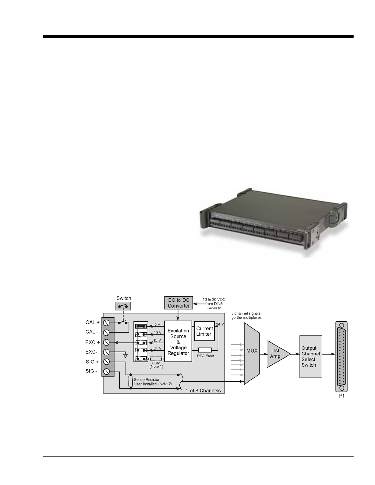
The DBK65 is an 8 channel transducer
interface module. Transducers of 2, 3, 4,
and 6 wire type can be easily connected
to the device by means of removable
screw terminal blocks, 1 per channel.
The module is ideally suited for
transducer outputs of the following
types. Wiring schematics are provided
on page 2 of this DBK65 section.
• 4 to 20 mA
• 3-wire string pots
• 4-wire bridge based transducers
• 6-wire bridge based transducers
BK65
DBK65 Block Diagram
Note 1: The user can install a resistor for use with the programmable regulator. The programmable voltage source can be
Note 2: The user can install a 250Ω resistor across the positive and negative signal lines (+Signal and -Signal) for
within the range of 5 to 20 VDC.
4 to 20 mA transducer outputs.
DBK Option Cards and Modules 987693 DBK65 pg. 1
Page 2
Each of the 8 channels can be set for a different excitation voltage. 5, 10, 15, and 24 VDC are provided
internally from the DBK65 and are selected via placement of a jumper. In addition, a fifth jumper position
can be used to select a custom voltage between 5 and 20 VDC. The user must install a resistor if this
option is desired. The following section, Customizing a Voltage, contains additional information.
Each channel includes 2 screw terminals that allow for a relay closure. Designated as CAL+ and
CAL-, the terminals can be used to switch in a calibration resistor for 6-wire transducers. Note that the
DBK65’s rear panel CAL switch will open or close the internal calibration switches for all 8 channels
simultaneously.
DBK65 Power Requirements
The amount of DC power required, which is supplied to the DBK65 through its Power-In DIN5 connector,
is 15 V @ 833 mA, 20 V @ 625 mA, assuming max load. In addition, the amount of power drawn from
the P1-based host acquisition device, such as a Daq device or a LogBook is 25 mA from ±15 V, 750 mW
total. For purpose of our discussion here, a P1-based device is one which is connecting to the DBK65 via
the DB37 (P1) connector.
Power Available for Transducers
At the excitation voltages available from the DBK65 (5 to 24 V) a single transducer will typically d raw
from 10 to 100mA. This fact and the per-channel and per-module current limits must be taken into account
to avoid overloading the system.
• Total current available, for all 8 channels: 240mA.
• Current available for a single channel: 100mA.
• Transducer, typical current draw: 10 to 100mA
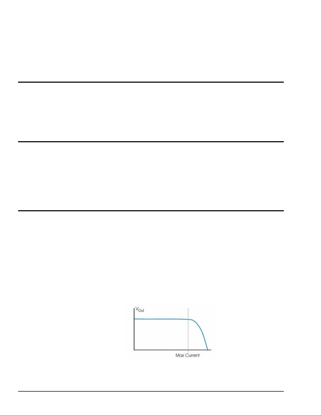
DBK65 Voltage Regulation
Better voltage regulation results in a lower variance of the source output voltage [excitation voltage], as
load is applied. Graphs depicting DBK65 voltage regulation for excitation set at 5, 10, 15, and 24 V are
included with the product’s specifications.
The following graph is intended to provide a better understanding of voltage regulation. In the graph, the
output voltage (V
This also applies to the user settable 5 to 20 VDC.
The ±5% variance factor holds true up to the limiting current (Max Current). Refer to the graphs at the end
of Specifications for typical voltage and current values.
) exhibits less than ±5% variance from nominal voltage, i.e., 5, 10, 15, or 24 VDC.
Out
Typical Current Limiting Voltage Curve
DBK65 pg. 2 987693 DBK Option Cards and Modules
Page 3
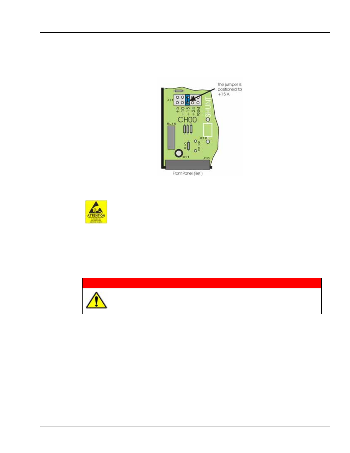
Selecting an Excitation Voltage
Each channel has a voltage select header, which consists of 5 pairs of pins and a jumper. The jumper
position determines the excitation voltage. Possible voltages are 5, 10, 1 5, and 24 VDC. A fifth possibility
exists for a custom voltage that resides within the range of 5 to 20 V. To obtain a custom voltage you must
install a resistor in the excitation line labeled “PGM.” The method is discussed shortly.
Reference for Selecting a Pre-Set Voltage Value
The discharge of static electricity can damage some electronic components.
Semiconductor devices are especially susceptible to ESD damage. You should
always handle components carefully, and you should never touch connector pins or
circuit components unless you are following ESD guidelines in an appropriate ESDcontrolled area. Such guidelines include the use of properly grounded mats and
wrist straps, ESD bags and cartons, and related procedures.
WARNING
To select a pre-set voltage (5, 10, 15, or 24V):
HOT COMPONENTS! Allow the DBK65 module to cool for at least 30 minutes
before removing the top cover. Some internal components can become very hot
and may cause burns.
1. Remove the DBK65 from power and disconnect all signal lines.
2. Allow the unit to cool for at least 30 minutes.
3. Remove the 4 screws from the top cover plate. Then remove the plate.
4. Position the voltage select header’s jumper to the desired setting. See the preceding figure.
5. Re-install the top cover plate and secure it with the 4 screws that were removed in step 3.
DBK Option Cards and Modules 987693 DBK65 pg. 3
Page 4
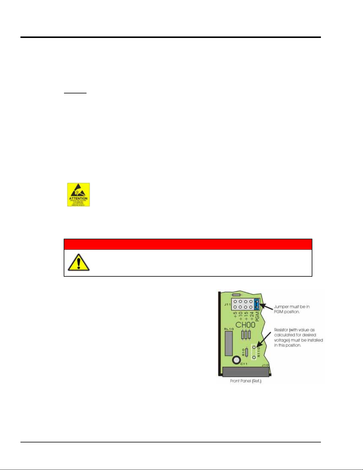
Customizing a Voltage
To make use of the custom voltage feature you will need to acquire a resistor of the calculated value. The
formula to use is:
= (V
R
2
Example:
Suppose you wanted an excitation source of 12V. Simply replace the V
R
. Thus, R2 = (12 - 1.2) / 0.007645 = 1412.688Ω Ιn practice, a 1400 ohm, 1% resistor would be used.
2
Of course, 1400Ω is a little off from the 1412.688Ω, which was calculated. To see the actual nominal
voltage that would result from 1400Ω we can use a second equation.
V
out
V
out
After the resistor value is known, it can be installed as follows.
– 1.2V) / 0.007645
out
= 1.2V (1 + R2/158) + 0.00005*R
= 1.2 (1 + 1400/158) + 0.00005*1400 = 11.903 volts
The discharge of static electricity can damage some electronic components.
Semiconductor devices are especially susceptible to ESD damage. You should
always handle components carefully, and you should never touch connector pins or
circuit components unless you are following ESD guidelines in an appropriate ESDcontrolled area. Such guidelines include the use of properly grounded mats and
wrist straps, ESD bags and cartons, and related procedures.
variable with 12V and solve for
out
2
WARNING
1. Remove the DBK65 from power and disconnect all
signal lines.
2. Allow the unit to cool for at least 30 minutes.
3. Remove the 4 screws from the top cover plate. Then
remove the plate.
4. Remove solder from the 2 holes at the resistor mounting
location.
5. Using rosin core solder and proper soldering technique,
solder the resistor into position for the applicable
channel. Be sure that the resistor leads are short
enough to avoid making contact with the metal
chassis.
The figure to the right indicates the resistor location for
use with channel 0 (CH00). The location scenario is similar
for all 8 channels.
Refer to the following table for a channel’s PGM Resistor Location
number. The location numbers appear on the circuit board.
HOT COMPONENTS! Allow the DBK65 module to cool for at least 30 minutes
before removing the top cover. Some internal components can become very hot
and may cause burns.
DBK65 pg. 4 987693 DBK Option Cards and Modules
Page 5
Channel PGM Resistor
Location
CH00 R110 J11
CH01 R120 J21
CH02 R130 J31
CH03 R140 J41
CH04 R150 J51
CH05 R160 J61
CH06 R170 J71
CH07 R180 J81
6. On the jumper header, reposition the channel’s voltage out jumper to the “PGM” position. Refer to
the table for a channel’s applicable Jumper Header. The header numbers appear on the circuit board.
7. If applicable, install resistors for other channels, and set the applicable voltage out jumper headers to
PGM.
8. Re-install the top cover plate and secure it with the 4 screws that were removed in step 3.
Creating a 4 to 20mA Current Loop
Voltage Out
Jumper Header
Voltage
Set
V
out
Resistor
Value
R
2
Inputs to monitor the commonly used 4 to 20mA current loops most often employ a 250Ω precision
resistor to develop a 1 to 5 VDC voltage drop.
Ideally, a resistor for such purpose should have a 0.1% tolerance (or better) with a minimum power rating
of 0.25W and a temperature coefficient of at least 25ppm/°C.
Lower values of resistance, for example, 62.5Ω [for a lower voltage drop within the loop of 0.25 to 1.25
VDC] will require that the host data acquisition device use a gain o f x4 to maximize the signal resolution.
The discharge of static electricity can damage some electronic components.
Semiconductor devices are especially susceptible to ESD damage. You should
always handle components carefully, and you should never touch connector pins or
circuit components unless you are following ESD guidelines in an appropriate ESDcontrolled area. Such guidelines include the use of properly grounded mats and
wrist straps, ESD bags and cartons, and related procedures.
WARNING
To create a 4 to 20mA current loop:
HOT COMPONENTS! Allow the DBK65 module to cool for at least 30 minutes
before removing the top cover. Some internal components can become very hot
and may cause burns.
1. Remove the DBK65 from power and disconnect all signal lines.
2. Allow the unit to cool for at least 30 minutes.
3. Remove the 4 screws from the top cover plate. Then remove the plate.
4. Remove solder from the 2 holes at the resistor mounting location (see the following figure for
location).
DBK Option Cards and Modules 987693 DBK65 pg. 5
Page 6

5. Using rosin core solder and proper soldering technique,
solder the resistor into position for the applicable
channel. Be sure that the resistor leads are short
enough to avoid making contact with the metal
chassis.
The figure to the right indicates the resistor location for
use with channel 0 (CH00). The location scenario is
similar for all 8 channels.
6. Re-install the top cover plate and secure it with the
4 screws that were removed in step 3.
Source Impedance and Settling Time
High speed multiplexing of signal sources with non-zero impedance will result in reading errors caused by
settling time. In the simplest form, a multiplexing system consists of a group of switches, with internal
resistance, and an output capacitance at the input of an amplifier feeding an A/D converter with a samplehold circuit on the input. During the short time a channel signal is connected to the A/D amplifier, the
signal must charge the output capacitance to the true value of the signal so that the sample-hold captures an
accurate value for the A/D converter to digitize. If the source has significant internal impedance the
voltage reading will be reduced.
Source impedance below 1000 ohms will create negligible error. Above 1000 ohms, the effects are
increasingly noticeable. An accurate source in series with a variable resistance will readily demonstrate
this. Although the effect is exponential, an easy reference point to remember is that 25K of source
impedance will result in approximately a 10% error.
Reading Error vs. Source Resistance
Source Resistance in Ohms
DBK65 pg. 6 987693 DBK Option Cards and Modules
Page 7

Configuring the DBK65 Address
You can connect 1 or 2 DBK65 modules to a single main channel on the primary data acquisition device.
Thus, a 16-channel Daq device can support up to 32 DBK65 modules. Since each module has 8 input
channels, a fully populated system can use 256 input sensors (32 modules x 8 channels per module).
To keep the large number of inputs organized, each DBK65 module is given a unique address via its DIP
switch, S1 [located on the rear panel].
Each DBK65 must be configured before connecting the module to inputs and outputs.
In addition, adjustment of the channel address must only be performed when the
system’s power is OFF. Failure to do so may result in equipment damage.
S1’s four leftmost micro-switches are used to set the module’s channel address in binary. Set the microswitches to the desired address only after ensuring that the system power is OFF. Several example address
settings are provided below. Other settings can be easily derived.
Each DBK65 module in the system must have a unique channel address for the primary
data acquisition device. Valid addresses are 0 to 15. Note that two modules can have a
setting for the same primary channel, for example, two modules could be set to channel
0; as long as one module is set to “L” to indicate the lower sub-channels 0-7 and the
other is set to “U” to indicate the upper sub-channels of 8-15. Examples of various
settings follow.
CAUTION
Channel 0 / Lower
Channel 5 / Lower
Channel 15 / Lower
Primary Acquisition Device Channel 0
DBK65 Lower Sub-Channels 0-7
The four leftmost micro-switches are set to “0” (Open). This sets the unit to
primary acquisition device Channel 0. The rightmost switch is at “L,”
setting the module to the “lower” DBK65 sub-channels (0 through 7).
Note: If connecting a second module to primary device Channel 0, the U/L
switch for that module would be set to “U” for sub-channels 8 thru 15.
Primary Acquisition Device Channel 5
DBK65 Lower Sub-Channels 0-7
The micro-switches for binary 4 and binary 1 are closed. This sets the unit to
primary acquisition device Channel 5. The rightmost switch is at “L,”
setting the module to the “lower” DBK65 sub-channels (0 through 7).
Primary Acquisition Device Channel 15
DBK65 Lower Sub-Channels 0-7
The micro-switches for binary 8, 4, 2, and 1 are closed, thus setting the
channel to “15” (8 + 4 + 2 + 1) for the primary acquisition device. The
rightmost switch is at “L,” setting the module to the “lower” DBK65 sub-
channels
(0 through 7).
Primary Acquisition Device Channel 2
DBK65 Upper Sub-Channels 8-15
Channel 2 / Upper
DBK Option Cards and Modules 987693 DBK65 pg. 7
The micro-switch for binary 2 is closed, thus setting the channel to “2” for the
primary acquisition device. The rightmost switch is at “U,” setting the module
to the “upper” DBK65 sub-channels (8 through 15).
Page 8

Configuring the Primary Data Acquisition Device
DaqBook/100 Series & /200 Series and DaqBoard [ISA type] Configuration
Use of a DBK65 with a DaqBook/100 Series, DaqBook/200 Series, or with an ISA-type DaqBoard device
requires the configuration of jumpers JP1 and JP4 located on that device, as applicable.
1. If not using auxiliary power, set the JP1 jumper for Analog Option Card Use [also referred to as the
expanded analog mode].
Note:
These jumpers do
not apply to /2000
Series Devices.
Required Jumper Settings for DaqBook/100 Series,
DaqBook /200 Series, and ISA-Type DaqBoards
The JP1 default position (above) is necessary to power the interface circuitry of the
DBK65 via the internal ±15 VDC power supply. If using auxiliary power you must
remove both JP1 jumpers.
2. For DaqBook/100, DaqBook /112, and DaqBook /120 only, place the JP4 jumper in the single-ended
mode.
Note: Analog expansion cards convert all input signals to single-ended voltages that are referenced to
analog common.
DaqBook/2000 Series & DaqBoard/2000 Series
No jumper configurations are required on the DaqBook/2000 series and DaqBoard/2000 series devices in
regard to connecting a DBK65.
LogBooks
No jumper configurations are required on LogBook devices in regard to connecting a DBK65.
DBK65 pg. 8 987693 DBK Option Cards and Modules
Page 9

Connecting the DBK65 to Signals and to the Primary Data Acquisition Device
You can connect the DBK65 module to your primary data acquisition device and to its signal inputs after
you have completed the following:
• set the DBK65 module’s address
• configured the DBK65 on a channel-by-channel basis for the application
• configured the primary data acquisition device, if applicable
You can connect up to eight sensors to one DBK65. A CA-37-x, CA-131-x, or a CA-255-xT cable is used
to connect the module to a LogBook or Daq device via DB37 connectors (P1).
To connect a DBK65 to a WaveBook or ZonicBook, refer to the final portion of this section, Connecting to
a BNC Connector.
If your system needs to be CE Compliant, be sure to read the applicable Declarations of
Conformity prior to connecting the DBK65.
Connect the DBK65 module as follows.
1. Connect each input to a screw terminal block on the DBK65. Example wiring diagrams are provided
below. Note that the screw-terminal blocks can be removed from the DBK65 to allow for easier
wiring.
CAUTION
Do not connect the excitation source to a non-isolated, powered transducer. Making
such a connection can cause damage to both the DBK65 and to the transducer.
Wiring Scenarios
A Note Regarding the Excitation Source
The excitation source is ground-referenced, not floating, i.e., the -Excitation (EXC -) terminal is connected
to the DBK65’s ground. The Excitation Source is designed to interface with transducers such that it is the
only power source, or its connection is electrically isolated from other power sources.
DBK Option Cards and Modules 987693 DBK65 pg. 9
Page 10

Tip: Label each transducer with its associated channel/sub-channel information.
2. For a single DBK65 module, connect one end of the P1 cable to the module’s male DB37 output
connector.
For DaqBook applications - use a CA-37-1, or a CA-255-xT cable. •
• • For DaqBoard/2000 Series applications - use a CA-37-1 with a DBK200 Series adapter.
For DaqBoard [ISA type] boards - use a CA-131-1 cable.
3. Connect the free end of the cable to the P1 port of the LogBook or Daq device. For multiple DBK65
modules, use a CA-37-x, CA-131-x, or a CA-255-xT cable to daisy-chain several modules or an
expansion module. For example, three DBK65s could be connected to a LogBook or a Daq device
with via a CA-37-3 cable.
Connecting to a BNC Connector (Used with WaveBooks and ZonicBooks)
To connect a BNC connector to a DBK65 channel as signal input we make use of the two-wire scenario.
The positive wire comes from the BNC central pin and connects to a DBK65 channel SIG+ terminal. The
negative wire connects the negative of the pin hub to a DBK65 channel SIG- terminal. A “BNC to Male
Binding Post” connector is convenient for making such two-wire connections.
Connecting a BNC to SIG+ and SIG- BNC to Male Binding Post (for 2-wire connection)
Software Setup
The DBK65 has no special software settings. The software controls are equivalent to those for a direct
connection; e.g., for a DaqBoard/2000 Series board there are Type selections of x1 to x64, representing the
internal gain of that board. When using the DBK6 5 with that board you will have the same Type options,
since the DBK65 is always a constant gain of x1.
LogView does not include the means to directly select a DBK65. To use a DBK65
with LogBook: First select DBK80 in LogView. This will recognize the DBK65, but
will identify it as a DBK80 (which has eight additional channels). Next do one of the
following as applicable:
(a) If the DBK65 is set to the L sub-address, use channels 0 through 7; and ignore
the displayed unused channels (8 through 15).
(b) If the DBK65 is set to the H sub-address, use channels 8 through 15; and
ignore the displayed unused channels (0 through 7).
Reference Notes:
o DaqView users - Refer to Chapter 3, DBK Setup in DaqView.
o LogView users - Refer to Chapter 4, DBK Setup in LogView. See above note.
DBK65 pg. 10 987693 DBK Option Cards and Modules
Page 11

Calibrating a Transducer using the “Shunt Calibration Technique”
The “shunt calibration” technique involves applying a known resistance across one leg of a transducer.
When the resistance is applied, the transducer’s output changes as it would if an actual load was applied.
Typically, transducers with internal amplifiers already have a built-in shunt calibration resistor. The shunt
calibration resistor can be activated via the DBK65 by use of its rear panel CAL switch.
Prior to making use of the CAL switch, two transducer wires must be connected from the transducer to the
applicable channel’s CAL+ and CAL- terminals on the DBK65. The wiring section of the transducer’s
calibration data sheet will indicate which terminals (or wires) are to be connected.
To perform shunt calibration:
1. Verify that each transducer to be calibrated has been properly connected to a DBK65
channel’s CAL+ and CAL- terminals.
2. Ensure that the transducer has no initial load, i.e., that it is initially at “zero.”
3. Adjust the data instruments zero-control to obtain a value of 0.0 volts.
In the case of 4 to 20 mA outputs, this value would be 4 mA.
4. Slide the CAL switch on the DBK65 rear panel to the “CLOSED” position. Each channel’s
internal calibration switch will simultaneously close, activating the calibration shunts [if
present].
A step change in the channel output will occur.
5. If the amount of the step change does not agree with the expected change as indicated by the
transducer’s calibration data sheet, adjust the transducer as needed. This is typically
accomplished with SPAN and/or GAIN control. Refer to the documentation for your specific
transducer.
6. Return the “CAL” switch to the “OPEN” position. This removes the shunt calibration
resistance from each channel.
7. Recheck the “zero.” Note that there may be some interaction if the GAIN or SPAN control
adjustments were large.
In regard to 4 to 20 mA circuits, several full cycles of adjusting the ZERO and SPAN controls
may be needed.
DBK Option Cards and Modules 987693 DBK65 pg. 11
Page 12

DBK65 Specifications
Dimensions: 285 mm W x 220 mm D x 45 mm H (11” x 8.5” x 1.75”)
Weight: 1.13 kg (2.5 lbs.)
Operating Temperature: -30°C to +70°C
System Connector: DBK37 male, mates with P1 connectors
Transducer Connectors: 8 removable screw-terminal blocks. Each block has 6 terminals.
Power Connectors: DIN5 Power In, DIN5 Power Out
DC Power Input: +10 to +30 VDC
DC Power Required (through DBK65 Power-In DIN5): 15 V @ 833 mA, 20 V @ 625 mA, assuming max load
DC Power Required (from P1-based host acqui sition device): 25 mA from ±15 V, 755 mW total
Gain Ranges: x1
Inputs: 8 differential voltage inputs
Maximum Voltage Range: ±10 V
Input Impedance: 20M Ohm
Accuracy: ±[0.025% +150 µV] (typ), ±[0.1% +250 µV] (max)
Noise: 60 µV
Temperature Coefficient: 10ppm for every degree outside the range of 0° to 50°C
Maximum Signal Input Voltage (without damage): ±35 V
3 dB Bandwidth: 2.6 MHz
CMRR: 80 dB (typ)
Output Voltage: Each channel, jumper-selectable to +5 V, +10 V, +15 V, and +24 V
or to a custom voltage setting within the range of +5 to +20 V (user set via resistor)
Voltage Accuracy: ±2% (typical)
Current Limit: 100 mA per channel
Load Regulation: 5% (typ)
Total Output: 240 mA max, total of all 8 channels
Accessories and Cables
Rack mount kit RackDBK3
Shielded P1 T cable for use with DaqBook/2020, LogBook/360, WBK40, WBK41 CA-255-4T
Shielded P1 T cable for use with DaqBook/2001, /2005, LogBook/300, DaqLab/2001, /2005 CA-255-2T
Ribbon cable for use with DaqScan CA-37-x (see note)
Note: The CA-37-x ribbon cable can also be used in lieu of the CA-255-x molded T cables.
The following 4 graphs illustrate the current limiting capabilities of the DBK65 for 5, 10, 15, and 24 VDC excitation
values.
DBK65 pg. 12 987693 DBK Option Cards and Modules
RMS
(typ)
Page 13

DBK65 I -V CURVE AT 5V EXCITA T ION
6.000
5.000
4.000
3.000
2.000
1.000
8
7
47
5
72
2
2
2
0
0
0
.
0.
0.
0
0.
4
8
05
2
2
0
47
3
3
3
0
0
0
.
.
0
0.
0.
0
2
02
7
4
3
0
0
.
0
7
5
3
79
2
4
4
5
0
0
0
.
0.
0
0.
0
CURRENT IN AMP S
7
85
61
62
5
7
6
0
0
0
.
.
0.
0
0.
4
9
90
6
8
0
86
0
1
1
1
1
.
0
1
0.
0.1
0.
0.000
00
2
1235
0.
VOLTS
V
DBK65 I- V CURVE AT 10V EX CITAT ION
12
10
8
VOLTS
V
0.0259
0.0
272
0.0
287
0.0303
0.0322
0.0344
0.0
367
0.0
394
427
0.0465
0.0
CURRENT IN AMPS
0.0511
0.0
564
0.0
631
0.0
718
0.0
833
0.0
992
0.1135
0.1
160
0.1
186
0.1
214
0.1
6
4
2
0
244
DBK65 I- V CURVE AT 15V EX CITAT ION
16
14
12
10
0.0
251
0.0
264
0.0
279
0.0295
0.0312
0.0
333
0.0
357
0.0
384
453
416
0.0
0.0
CURRENT IN AMPS
0.0
498
0.0
551
0.0
618
0.0705
0.0817
0.0974
0.1
118
0.1
146
0.1177
0.1211
8
6
4
2
0
0.1246
V
V
DBK65 I- V CURVE AT 24V EX CITAT ION
25
20
15
10
5
0
0.0
249
0.0262
0.0
276
0.0292
0.0310
0.0
330
0.0353
0.0
380
450
0.0
0.0412
CURRENT IN AMPS
0.0494
0.0548
0.0
616
0.0
703
0.0817
0.0
975
0.1
210
0.1
596
0.2046
0.2
666
0.0
000
V
V
DBK Option Cards and Modules 987693 DBK65 pg. 13
Page 14

DBK65 pg. 14 987693 DBK Option Cards and Modules
 Loading...