

Page 1
DBK45 4-Channel SSH and Low-Pass Filter Card
Overview …… 1
Hardware Setup …… 2
Card Connection …… 2
Card Configuration …… 2
Configuring DBK45 Filter Sections …… 3
DaqBook/100 Series & /200 Series and DaqBoard [ISA type] Configuration …… 5
DaqBook/2000 Series and DaqBoard/2000 Series Configuration …… 5
Software Setup …… 5
DBK45 – Specifications …… 6
Reference Notes:
o Chapter 2 includes pinouts for P1, P2, P3, and P4. Refer to pinouts applicable to your
Overview
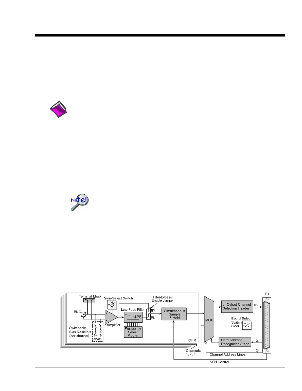
The DBK45 combines the features of the DBK17 (SSH) and the DBK18 (low-pass filter) cards. Each
DBK45 provides 4 input channels to a LogBook or Daq device system. Each of the main 16 analog input
channels can accept four DBK45s, for a maximum of 64 DBK45s and 256 analog input channels. The
simultaneous sample-hold function is activated at the beginning of each channel scan and freezes all
signals present on DBK45 inputs for the duration of the scan, allowing for non-skewed readings of all
channels.
system, as needed.
o In regard to calculating system power requirements, refer to DBK Basics located near
the front of this manual.
You should never set a DBK45 channel as the 1st channel in a scan due to timing of
the SSH line.
For each of the four channels, a separate filter and a sample-hold stage follow the input stage. The outputs
are connected to a 4-channel multiplexer stage. The enabled-output MUX allows four DBK45s to share a
common analog input channel.
The DBK45 has an instrumentation amplifier for each channel, with switch-selected gains of ×1, ×10,
×100, ×200 and ×500. A socket is provided for a gain resistor for custom gain-selection instead of the 5
factory-default gains. Gain for any channel can be set to any value between unity and ×500 by installing
an appropriate resistor. Four separate filter stages follow the 4 input stages. The outputs are connected to
a
4-channel multiplexer stage. The enabled output MUX allows four DBK45s to share a common analog
base channel.
Input can be connected to a channel’s BNC or terminal block connector. The differential inputs are
provided with switchable 100 kΩ bias resistors to analog common.
DBK Option Cards and Modules 987696 DBK45, pg. 1
Page 2
Hardware Setup
Card Connection
DBK45 Block Diagram
DBK45 is equipped with a BNC connector for each of the four differential analog inputs. The card
includes terminal block connections, which can be used instead of the BNC connectors if desired.
Card Configuration
Factory Defaults:
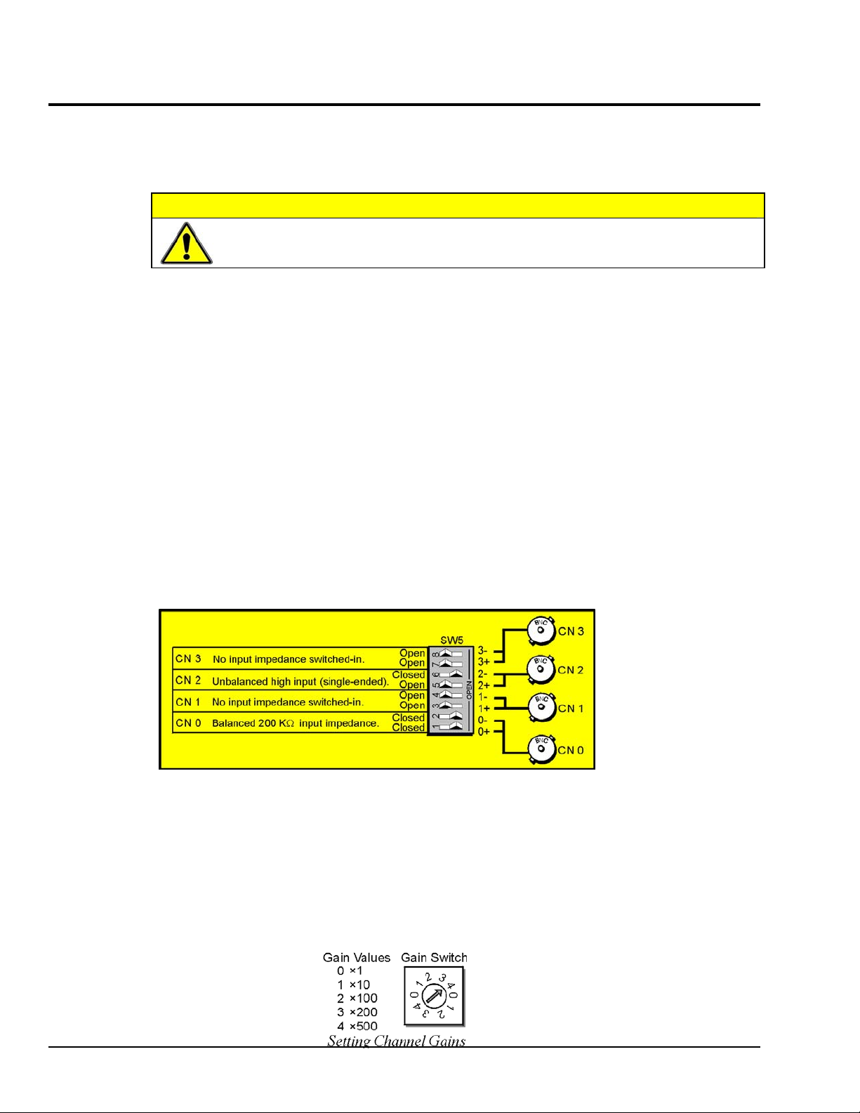
Input Termination
DBK45 provides two 100 KΩ bias resistors for each analog input. For balanced 200 KΩ input
impedance, both resistors should be switched in. An 8-position DIP switch (SW5) can selectively engage
the bias resistors. The switches must be in the closed position to engage the termination resistors. For
unbalanced high input, only the (-) resistor should be used. If neither resistor is used, some external bias
current path is required. Examples of SW5 switch positions and the resulting impedance selection
follows.
CAUTION
Input voltage levels must not exceed ±5 V bipolar or 10 V unipolar.
• 100K bias resistors – Enabled
• Low pass filter – Disabled (bypassed)
• Gain – x1
• SSH - Enabled
Examples of Bias Resistor Selection Options
Gain Settings
On the printed circuit board, each channel has one gain-set switch. The switches are labeled GAIN 1,
GAIN 2, GAIN3, and GAIN 4. Each channel also has holes in the board for gain resistors labeled RG1 to
RG4. The 5 gain values for switch settings 0 to 4 are provided in the following figure. If a custom gain is
desired, the switch is set to position 0; and a gain resistor must be mounted and soldered onto the board.
The gain resistor’s value is determined by the formula: R
DBK45, pg. 2 987696 DBK Option Cards and Modules
= [40,000 / (Gain -1)] - 50 Ω
GAIN
Page 3

Address Configuration
Up to four DBK45s can be connected to each analog channel. With
16 main channels and 4 inputs per DBK45, 256 inputs are possible. Since this is
a daisy-chain interface, each DBK45 must have a unique address (channel and
card number). Note that the default setting of SW6 is Card 1.
To configure the module, locate the 16 × 2-pin header (labeled J1) near the front
of the board (near P1). The 16 jumper locations on this header are labeled CH0
through CH15. Place the jumper on the channel you wish to use. Only one
jumper is used.
Note: Two DBK45s in the daisy-chain can have the same channel number as
long as their card number is unique.
Set switch SW6 for each DBK45 on a single channel. Verify that only one card
in the system is set to a particular channel and card number.
Configuring DBK45 Filter Sections
There are 4 low-pass, 3-pole active filters on the DBK45. Each filter can be enabled (EN) or bypassed
(BY) by placement of the jumper on J3 for channel 0, J4 for channel 1, J5 for channel 2, J6 for
channel 3. The factory-default setting is enabled (EN) for each channel. Each filter can be configured as
a Butterworth, Bessel, or Chebyshev filter with corner frequencies up to 50 kHz. Filter properties depend
on the values of resistors and capacitors installed in several circuit locations. Above 10 Hz, installing
capacitors is unnecessary because capacitors in the ICs are sufficient. In all cases, three resistors are
required to complete the active filter circuits contained mostly within the UAF42 ICs.
The following circuit diagram shows the active filter IC in a typical section of the DBK45. The resistors
and capacitors outside the IC have a physical location in a DIP-16 socket (dual in-line, 16 pins) with an
RCnn designator. The RC indicates the needed part is a resistor or capacitor; the 3rd character is the
channel number; and the 4th character corresponds to the socket position (A-H).
Filter Circuit Diagram
A machined-pin IC socket in each filter RC location can accept resistors and capacitors that plug directly
into the socket; however, this is not recommended. Two much better approaches exist. The first is to use
pre-configured plug-in filter modules; the second is to configure your own plug-in module using a blank
CN-115. Both of these options are illustrated on the following page.
The use of plug-in modules provides excellent “gold-to-gold” contact between the components of the plugin module and the on-board header.
DBK Option Cards and Modules 987696 DBK45, pg. 3
Page 4

The right-hand figure shows the DIP-16
component pattern typical of the 4 filter sections.
Note: “n” corresponds to “channel number.”
Pin 7 of the DIP-16 socket:
• connects to pin 8 for low-pass filtering
• connects to pin 6 for band-pass filtering
DIP-16 Component Pattern
The following table lists values of components for common corner frequencies in Butterworth filters. If
designing your own filter, software from Burr-Brown provides the component values to create the desired
filter. Note that the design math is beyond the scope of this manual.
3-Pole Butterworth Filter Components
3dB
(Hz)
0.05
0.10
0.20
0.50
1
2
5*
10*
20
50
100*
200
500*
1000*
2000
5000
10000
*These pre-configured Butterworth frequency modules are available from the manufacturer.
RCnA RCnB RCnC RCnD RcnE RCnF RCnG RCnH
3.16 MΩ
1.58 MΩ
787 kΩ
3.16 MΩ
1.58 MΩ
787 kΩ
3.16 MΩ
1.58 MΩ
787 kΩ
3.16 MΩ
1.58 MΩ
787 kΩ
316 kΩ
158 kΩ
78.7 kΩ
31.6 kΩ
15.8 kΩ
1 µF none
1 µF none
1 µF none
0.1 µF none
0.1 µF none
0.1 µF none
0.01 µF none
0.01 µF none
0.01 µF none
0.001 µF none
0.001 µF none
0.001 µF none
0.001 µF none
0.001 µF none
0.001 µF none
0.001 µF none
0.001 µF none
3.16 MΩ
1.58 MΩ
787 kΩ
3.16 MΩ
1.58 MΩ
787 kΩ
3.16 MΩ
1.58 MΩ
787 kΩ
3.16 MΩ
1.58 MΩ
787 kΩ
316 kΩ
158 kΩ
78.7 kΩ
31.6 kΩ
15.8 kΩ
1 µF
1 µF
1 µF
0.1 µF
0.1 µF
0.1 µF
0.01 µF
0.01 µF
0.01 µF
none
none
none
none
none
none
none
none
3.16 MΩ
1.58 MΩ
787 kΩ
3.16 MΩ
1.58 MΩ
787 kΩ
3.16 MΩ
1.58 MΩ
787 kΩ
3.16 MΩ
1.58 MΩ
787 kΩ
316 kΩ
158 kΩ
78.7 kΩ
31.6 kΩ
15.8 kΩ
none 1 µF
none 1 µF
none 1 µF
none 0.1 µF
none 0.1 µF
none 0.1 µF
none 0.01 µF
none 0.01 µF
none 0.01 µF
none none
none none
none none
none none
none none
none none
none none
none none
You have the option to configure the filter sections as b and-pass filters rather than low-pass filters. The
component selection program provides band-pass component values. The program also computes and
displays phase and gain characteristics of the filter sections as a function of freq uency.
DBK45, pg. 4 987696 DBK Option Cards and Modules
Page 5

DaqBook/100 Series & /200 Series and DaqBoard [ISA type] Configuration
Use of the DBK45 requires setting jumpers in DaqBooks/100 Series & /200 Series devices and
ISA-type DaqBoards.
1. If not using auxiliary power, set the JP1 jumper for Analog Option Card Use (also referred to
as Analog Expansion Mode).
Note:
These jumpers do not
apply to /2000 Series
devices.
Jumpers on DaqBook/100 Series, DaqBook/200 Series, and ISA-type DaqBoards
The JP1 default position (Analog Option Card Use) is necessary to power the interface
circuitry of the DBK45 via the internal ±15 VDC power supply. If using auxiliary
power, e.g., DBK32A or DBK33, you must remove both JP1 jumpers. Refer to
Power Requirements in the DBK Basics section and the DBK32A and DBK33 sections for
more information, as applicable.
2. Place the JP2 jumper in the SSH position.
Do not use an external voltage reference for DAC1. Applying an external voltage
CAUTION
reference for DAC1, when using the SSH output, will result in equipment damage
due to a conflict on P1, pin #26.
3. For DaqBook/100, DaqBook/112 and DaqBook/120
only, place the JP4 jumper in
single-ended mode.
DaqBook/2000 Series and DaqBoard/2000 Series Configuration
No hardware configuration is required for DaqBook/2000 Series or DaqBoard/2000 Series devices.
Software Setup
Reference Notes:
o DaqView users - Refer to chapter 3, DBK Setup in DaqView.
o LogView users - Refer to chapter 4, DBK Setup in LogView.
DBK Option Cards and Modules 987696 DBK45, pg. 5
Page 6

DBK45 – Specifications
Name/Function: Simultaneous Sample and Hold and
Low-Pass Filter Card
Number of Channels: 4
Input Connections: 4 BNC connectors; 4 screw-terminal sets
Output Connector: DB37 male,
mates with P1 using CA-37-x cable
Number of Cards Addressable: 64
Dimensions: 8.25” × 3.25”
Input Type: Differential
Voltage Input Ranges:
0 to ±5000 mVDC
0 to ±500 mVDC
0 to ±50 mVDC
0 to ±25 mVDC
0 to ±10 mVDC
For Custom Gains: R
Input Amplifier Slew Rate: 12 V/µs minimum
Acquisition Time:
0.6 µs (10 V excursion to 0.1%)
0.7 µs (10 V excursion to 0.01%)
Channel-to-Channel Aperture Uncertainty: 50 ns
Output Droop Rate: 0.1 µV/µs
Input Gains: ×1, ×10, ×100, ×200, x500, and
user-set up to ×500
Input Offset Voltage: 500 µV + 5000/G maximum (nullable)
Input Offset Drift: ±5 + 100/G µV/°C maximum
Input Bias Current: 100 pA maximum
Input Offset Currents: 50 pA maximum
Input Impedance: 5 × 10
Switchable Bias Resistors: 100 KΩ each to analog common
= [40,000/(Gain-1)] - 80 Ω
GAIN
12
Ω parallel with 6 pF
Gain Errors:
0.04% @ ×1
0.1% @ ×10
0.2% @ ×100
0.4% @ ×200
1.0% @ ×500
Temperature vs Gain:
±20 ppm/°C @ ×1
±20 ppm/°C @ ×10
±40 ppm/°C @ ×100
±60 ppm/°C @ ×200
±100 ppm/°C @ ×500
Non-Linearity:
±0.015 % full-scale @ ×1
±0.015 % full-scale @ ×10
±0.025 % full-scale @ ×100
±0.025 % full-scale @ ×200
±0.045 % full-scale @ ×500
Common-Mode Rejection:
70 dB minimum @ ×1
87 dB minimum @ ×10
100 dB minimum @ ×100
100 dB minimum @ ×200
100 dB minimum @ ×500
Active Filter Device: UAF42 (Burr-Brown)
Number of Poles/Filter: 3
Types of Filters: Bessel, Butterworth,
Chebyshev
Frequency Range: 0.1 Hz to 50 kHz
The frequency is set by installation of
4-6 resistors and/or capacitors in
provided socket locations.
Frequency Modules: Optional frequency
module kits are available that consist of
4 plug-in resistor/capacitor (RC)
headers. These RC headers are preconfigured for any of the following
frequencies: 5 Hz, 10 Hz, 100 Hz,
500 Hz, or 1 kHz—all are Butterworthtype filters.
DBK45, pg. 6 987696 DBK Option Cards and Modules
 Loading...