

Page 1
DBK206 P4-to-P1/P2/P3 Adapter Board
For Analog I/O, Digital I/O, & Pulse/Frequency
Overview …… 1
Connections …… 1
Note:
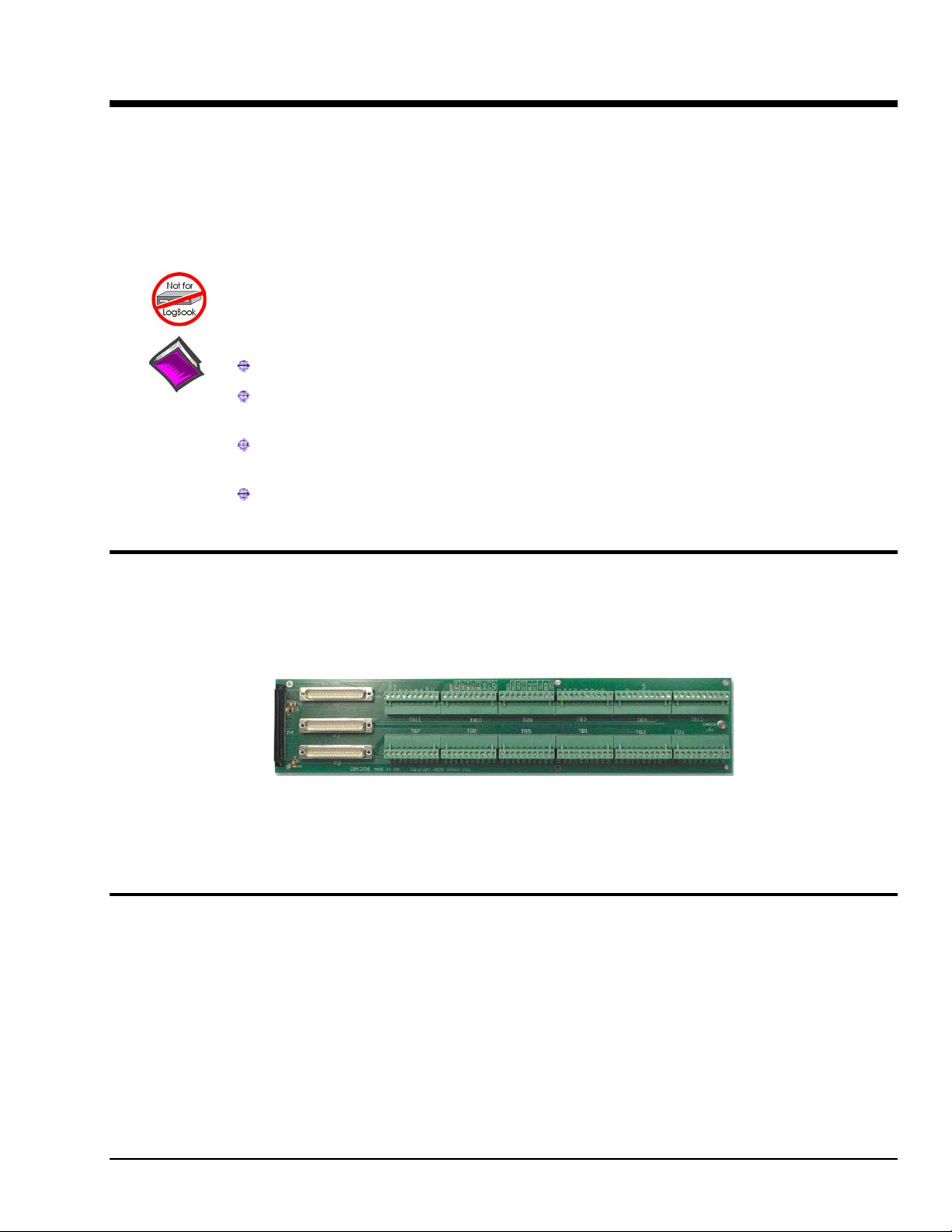
DBK206 provides: P1, P2, and P3 connectors and corresponding screw-terminal blocks
for use with DaqBook/2000 Series Devices, DaqBoard/2000 Series Boards,
and cPCI DaqBoard/2000c Series Boards.
This product is not used for LogBook applications.
Reference Notes:
In regard to calculating system power requirements refer to the DBK Basics section.
Chapter 2 includes pinouts for P1, P2, P3, and P4. Refer to pinouts applicable to your
system, as needed.
For a quick comparison of all DBK200 Series boards, refer to the DBK200 Series Matrix.
The matrix is located just before the DBK200 section.
Refer to the DaqBoard/2000 Series and cPCI DaqBoard/2000c Series User’s Manual
(p/n 1033-0901) or the DaqBook/2000 Series User’s Manual (p/n 1103-0901)
for information pertaining to those products, as needed.
Overview
DaqBoard/2000 Series and cPCI DaqBoard/2000c Series boards communicate [external from the host PC]
through a 100-pin P4 connector. The DBK206 provides a P1, P2, and P3 connector and corresponding
screw-terminal blocks. P1 is used for ANALOG I/O, P2 for DIGITAL I/O, and P3 for
PULSE/FREQUENCY (Digital and Counter/Timer) I/O.
Note: The P1, P2, and P3 connectors discussed in association with DaqBook/2000 Series devices
Connections
The DBK206 is suitable for both analog and digital expansion. Signal connection to a DaqBook/2000
Series device, DaqBoard/2000 Series board, or to a cPCI DaqBoard/2000c Series board can be made as
follows:
DBK206, P4-to-P1/P2/P3 Adapter with Screw-Terminals
DaqBoard/2000 Series boards and cPCI DaqBoard/2000c Series boards are subset connectors of the
100-pin P4 connector that is located on those boards. Chapter System Connections and Pinouts,
includes pinouts for P1, P2, P3, and P4.
• With cables connected to P1, P2, and P3 connectors, as applicable.
• With signal wires connected to the appropriate screw-terminal blocks (TB1 through TB12).
Note that the DBK206 board’s silkscreen clearly identifies all screw terminals.
• With a combination of the above two methods.
DBK Option Cards and Modules 987594 DBK206, pg. 1
Page 2
Regardless of which method is used, the DBK206 connects to the 100-pin P4 connector of a
DaqBook/2000 Series device, DaqBoard/2000 Series board, or a cPCI DaqBoard/2000c Series board. The
connection is made via a CA-195 cable. Note that DBK206 contains mounting holes that allow the board
to be secured inside a user-provided enclosure (not shown).
CAUTION
Turn off power to the host PC and externally connected equipment prior to connecting
cables or signal lines to the DBK. Electric shock or damage to equipment can result
even under low-voltage conditions.
Take ESD precautions (packaging, proper handling, grounded wrist strap, etc.)
Use care to avoid touching board surfaces and onboard components. Only handle
boards by their edges (or ORBs, if applicable). Ensure boards do not come into contact
with foreign elements such as oils, water, and industrial particulate.
Do not confuse connectors. Ensure that you only connect P1 I/Os to P1,
P2 I/Os to P2, and P3 I/Os to P3. Improper connection may result in equipment
damage.
The illustrations and actual board silkscreen are the only references you should need to make proper
connections.
A list of connection tips follows:
1. Ensure power is removed from the device(s) to be connected.
2. Observe ESD precautions when handling the board and making connections.
3. Do not make redundant connections. For example, for ANALOG IN you can use the P1
(DB37) connector or Terminal Blocks TB9 through TB12. You would not use both sets of
ANALOG IN connectors.
DBK206, pg. 2
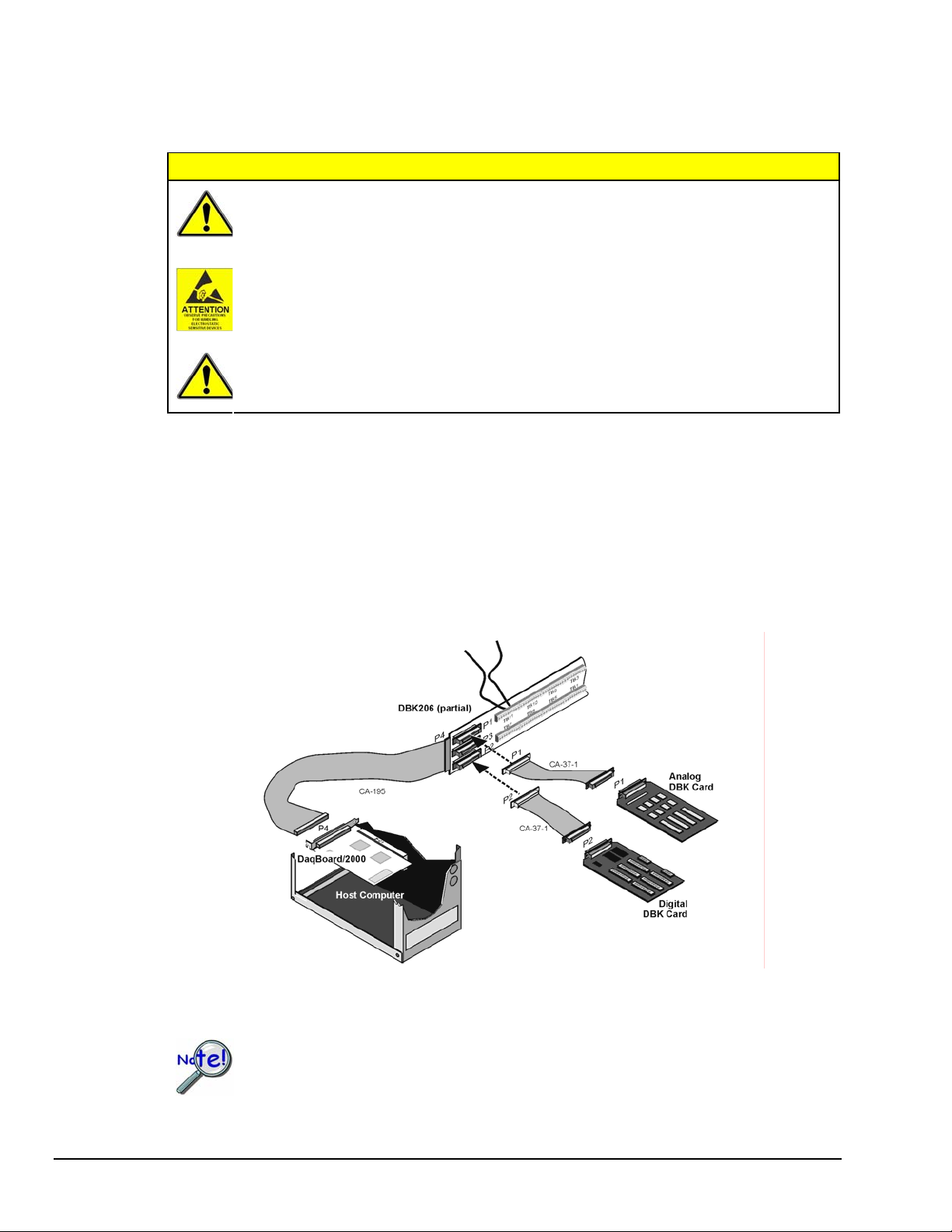
Example of a DBK206 Connected to Analog and Digital DBK Cards
Through P1 and P2, Respectively
Be sure to align the P4 orientation indicators () prior to mating the P4 connectors.
4. The DBK206 100-pin P4 connector connects to the DaqBoard/2000 Series P4 connector via a
CA-195 Cable.
987594 DBK Option Cards and Modules
Page 3

5. To obtain maximum protection from static, connect the CHASSIS terminal to earth ground.
6. For connections to DB37 connectors:
• P1 connects to an analog DBK card or module’s P1 connector via a CA-37 cable.
• P2 connects to a Digital DBK card or module’s P2 connector via a CA-37 cable.
• P3 connects to a Pulse/Frequency DBK card or module’s P3 connector via a CA-37
cable.
7. In regard to Screw-Terminal Block Connections:
• When tightening terminal block screws, tighten them snug, but do not over-tighten.
• The DBK206 includes 12 terminal blocks. Each block contains 10 screw-terminal
connectors.
• The DBK206 silkscreen provides labels for each terminal block (TB1 through
TB12) and for each of the block’s associated screw-terminals.
• TB9, TB10, TB11, and TB12 are used for ANALOG IN and provide a connection
option to the P1 (DB37) connector.
• TB5, TB6, TB7, and TB8 are used for DIGITAL I/O and provide a connection
option to the P2 (DB37) connector.
• TB1, TB2, TB3, and TB4 are used for Pulse/Frequency/Digital I/O and provide a
connection to the P3 (DB37) connector.
• The following pages correlate the DBK206 terminal block connectors with the
associated pins of the P1, P2, and P3 DB37 connectors. Note that the
System Connections and Pinouts chapter contains additional pin-outs, and includes
references to the 100-pin P4 connector.
DBK Option Cards and Modules 987594 DBK206, pg. 3
Page 4

Correlation to P1 – TB11, TB10, TB9, and TB12 for Analog I/O.
TB11 P1 Pin Number and Description
TTL TRIG 25 TTL Trigger, Digital IN, External TTL Trigger Input
A/I CLK 20 A/I Clock, External ADC Pacer Clock Input/
EXP 5 5 Expansion 5. Digital OUT, external GAIN select bit 1
EXP 6 6 Expansion 6. Digital OUT, external GAIN select bit 0
EXP 7 3 Expansion 7. Digital OUT, external ADDRESS, select bit 3
EXP 8 22 Expansion 8. Digital OUT, external ADDRESS, select bit 2
EXP 9 4 Expansion 9. Digital OUT, external ADDRESS, select bit 1
EXP 10 23 Expansion 10. Digital OUT, external ADDRESS, select bit 0
EXP 11 26 Expansion 11. Simultaneous Sample and Hold (SSH)
AGND * Analog Common
TB10 P1 Pin Number and Description
SGND 19 Signal Ground, Sense Common
POSREF 9 Positive Reference, Analog +5 V reference
SE15 11 CH 15 IN (Single-Ended Mode) / CH 7 LO IN (Differential Mode)
SE7 30 CH 7 IN (Single-Ended Mode) / CH 7 HI IN (Differential Mode)
SE14 12 CH 14 IN (Single-Ended Mode) / CH 6 LO IN (Differential Mode)
SE6 31 CH 6 IN (Single-Ended Mode) / CH 6 HI IN (Differential Mode)
SE13 13 CH 13 IN (Single-Ended Mode) / CH 5 LO IN (Differential Mode)
SE5 32 CH 5 IN (Single-Ended Mode) / CH 5 HI IN (Differential Mode)
SE12 14 CH 12 IN (Single-Ended Mode) / CH 4 LO IN (Differential Mode)
SE4 33 CH 4 IN (Single-Ended Mode) / CH 4 HI IN (Differential Mode)
TB9 P1 Pin Number and Description
SGND 19 Signal Ground, Sense Common
NEGREF 8 Negative Reference, Analog -5 V reference
SE11 15 CH 11 IN (Single-Ended Mode) / CH 3 LO IN (Differential Mode)
SE3 34 CH 3 IN (Single-Ended Mode) / CH 3 HI IN (Differential Mode)
SE10 16 CH 10 IN (Single-Ended Mode) / CH 2 LO IN (Differential Mode)
SE2 35 CH 2 IN (Single-Ended Mode) / CH 2 HI IN (Differential Mode)
SE9 17 CH 9 IN (Single-Ended Mode) / CH 1 LO IN (Differential Mode)
SE1 36 CH 1 IN (Single-Ended Mode) / CH 1 HI IN (Differential Mode)
SE8 18 CH 8 IN (Single-Ended Mode) / CH 0 LO IN (Differential Mode)
SE0 37 CH 0 IN (Single-Ended Mode) / CH 0 HI IN (Differential Mode)
TB12 P1 Pin Number and Description
AGND * Analog Common
AGND * Analog Common
AGND * Analog Common
AGND * Analog Common
AGND * Analog Common
AGND * Analog Common
+ 15 V 21 Expansion, +15 V Power
- 15 V 2 Expansion, -15 V Power
AGND * Analog Common
+ 5 V 1 Expansion, +5 V Power
* Refer to Ground Correlation Tables in the System Connections and Pinouts chapter.
Internal ADC Pacer Clock Output
DBK206, pg. 4
987594 DBK Option Cards and Modules
Page 5

Correlation to P2 – TB5, TB6, TB7, and TB8 for Digital I/O.
TB7 P2 Pin Number and Description
C0 29 Digital I/O: P2, Digital Port C, Bit 0; or P2 Expansion Data Bit 0
C1 28 Digital I/O: P2, Digital Port C, Bit 1; or P2 Expansion Data Bit 1
C2 27 Digital I/O: P2, Digital Port C, Bit 2; or P2 Expansion Data Bit 2
C3 26 Digital I/O: P2, Digital Port C, Bit 3; or P2 Expansion Data Bit 3
C4 25 Digital I/O: P2, Digital Port C, Bit 4; or P2 Expansion Data Bit 4
C5 24 Digital I/O: P2, Digital Port C, Bit 5; or P2 Expansion Data Bit 5
C6 23 Digital I/O: P2, Digital Port C, Bit 6; or P2 Expansion Data Bit 6
C7 22 Digital I/O: P2, Digital Port C, Bit 7; or P2 Expansion Data Bit 7
DGND * Digital Common
DGND * Digital Common
TB8 P2 Pin Number and Description
B7 3 Digital I/O: P2, Digital Port B, Bit 7; or P2 Expansion Address Bit 0 Out
B6 4 Digital I/O: P2, Digital Port B, Bit 6; or P2 Expansion Address Bit 1 Out
B5 5 Digital I/O: P2, Digital Port B, Bit 5; or P2 Expansion Address Bit 2 Out
B4 6 Digital I/O: P2, Digital Port B, Bit 4; or P2 Expansion Address Bit 3 Out
B3 7 Digital I/O: P2, Digital Port B, Bit 3; or P2 Expansion Address Bit 4 Out
B2 8 Digital I/O: P2, Digital Port B, Bit 2; or P2 Expansion RESET Output
B1 9 Digital I/O: P2, Digital Port B, Bit 1; or P2 Expansion WRITE Output
B0 10 Digital I/O: P2, Digital Port B, Bit 0; or P2 Expansion READ Output
DGND * Digital Common
DGND * Digital Common
TB5 P2 Pin Number and Description
DGND * Digital Common
DGND * Digital Common
A7 30 Digital I/O: P2, Digital Port A, Bit 7; or P2 Expansion Data Bit 15
A6 31 Digital I/O: P2, Digital Port A, Bit 6; or P2 Expansion Data Bit 14
A5 32 Digital I/O: P2, Digital Port A, Bit 5; or P2 Expansion Data Bit 13
A4 33 Digital I/O: P2, Digital Port A, Bit 4; or P2 Expansion Data Bit 12
A3 34 Digital I/O: P2, Digital Port A, Bit 3; or P2 Expansion Data Bit 11
A2 35 Digital I/O: P2, Digital Port A, Bit 2; or P2 Expansion Data Bit 10
A1 36 Digital I/O: P2, Digital Port A, Bit 1; or P2 Expansion Data Bit 9
A0 37 Digital I/O: P2, Digital Port A, Bit 0; or P2 Expansion Data Bit 8
TB6 P2 Pin Number and Description
+5 V 18 Expansion +5 V Power
+5 V 20 Expansion +5 V Power
DGND * Digital Common
DGND * Digital Common
DGND * Digital Common
DGND * Digital Common
DGND * Digital Common
DGND * Digital Common
DGND * Digital Common
DGND * Digital Common
* Refer to Ground Correlation Tables in the System Connections and Pinouts chapter.
DBK Option Cards and Modules 987594 DBK206, pg. 5
Page 6

Correlation to P3 – TB1, TB2, TB3, and TB4 for Pulse/Frequency/Digital I/O.
TB1 P3 Pin Number and Description
D8 29 P3 Digital Port Bit 8
D9 28 P3 Digital Port Bit 9
D10 27 P3 Digital Port Bit 10
D11 26 P3 Digital Port Bit 11
D12 25 P3 Digital Port Bit 12
D13 24 P3 Digital Port Bit 13
D14 23 P3 Digital Port Bit 14
D15 22 P3 Digital Port Bit 15
DGND * Digital Common
DGND * Digital Common
TB2 P3 Pin Number and Description
D0 10 P3 Digital Port Bit 0
D1 9 P3 Digital Port Bit 1
D2 8 P3 Digital Port Bit 2
D3 7 P3 Digital Port Bit 3
D4 6 P3 Digital Port Bit 4
D5 5 P3 Digital Port Bit 5
D6 4 P3 Digital Port Bit 6
D7 3 P3 Digital Port Bit 7
DGND * Digital Common
+5V 20 Expansion, +5 Volt Power
TB4 P3 Pin Number and Description
EXP 2 12 Reserved
EXP 3 13 Reserved
EXP 4 14 Reserved
TMR 0 15 P3 Timer 0 Output
TMR 1 16 P3, Timer 1 Output
CNT 3 35 P3 Counter 3 Input
CNT 2 17 P3 Counter 2 Input
CNT 1 36 P3 Counter 1 Input
CNT0 18 P3 Counter 0 Input
DGND * Digital Common
TB3 P3 Pin Number and Description
DAC0 34 Analog Out; Analog DAC 0 Output
AGND * Analog Common
DAC2 32 Analog Out; Analog DAC 2 Output
AGND * Analog Common
DAC1 33 Analog Out; Analog DAC 1 Output
A/O CLK 21 Analog Out Clock; External DAC Pacer Clock Input/
DAC3 31 Analog Out; Analog DAC 3 Output
DGND * Digital Common
+15 V 19 Expansion, + 15 VDC
-15 V 37 Expansion, -15 VDC
* Refer to Ground Correlation Tables in the System Connections and Pinouts chapter.
Internal DAC Pacer Clock Output
DBK206, pg. 6
987594 DBK Option Cards and Modules
 Loading...