

Page 1
DBK202, DBK203, DBK204 Series P4-to-P1 / P2 / P3 Adapters
For Analog I/O, Digital I/O, & Pulse/Frequency For Use with DaqBook/2000 Series or
DaqBoard/2000 Series Devices
Overview …… 2
Connection Tips…… 4
Using Screw-Terminal Blocks …… 6
Using the P3 Header …... 11
Adding Resistor/Capacitor
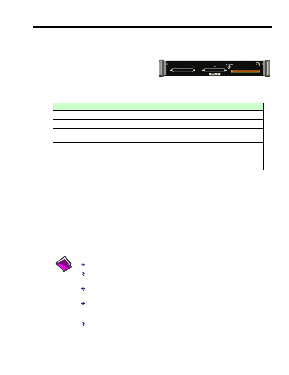
Filter Networks …… 12 DBK203A, Rear Panel
DBK Decription
DBK202
Screw-terminal adapter board. Board only, no chassis.
DBK203
DBK203A
DBK204
DBK204c
Each of these units includes:
(a) P1, Analog Input, DB37 connector
(b) P2, Digital I/O DB37 connector
(c) P3, internal 40-pin header, for Digital I/O and Analog Out. The 40-pin header connects to a
Pulse/Frequency DBK card, or to a module’s P3 connector via a
CA-60 cable. These cables have a 40-pin female connector at one end and a DB37 (37-pin)
male connector at the other end.
(d) P4, 100-pin connector which includes all signals found in P1, P2, and P3, collectively.
(e) Internal, on-board, screw-terminal blocks which correlate with P1, P2, and P3
Screw-terminal adapter module with pull-out drawer. Superseded by DBK203A.
Screw-terminal adapter module (supersedes DBK203). DBK203A is the most popular of
these 5 DBK options.
DBK203A plus CA-209 CE cable kit. DBK204 units shipped prior to the release of
DBK203A use a DBK203.
DBK203A plus CA-209c CE cable kit. For use with compact PCIs and DaqBoard/2000c
Series boards. DBK204c units shipped prior to the release of DBK203A use a DBK203.
(f) Internal, on-board socket locations for custom RC Filter networks
Reference Notes:
In regard to calculating system power requirements refer to the DBK Basics section.
Chapter 2 includes pinouts for P1, P2, P3, and P4. Refer to pinouts applicable to your
system, as needed.
For a quick comparison of all DBK200 Series boards, refer to the DBK200 Series Matrix.
The matrix is located just before the DBK200 section.
Refer to the DaqBoard/2000 Series User’s Manual (p/n 1033-0901) or the
DaqBook/2000 Series User’s Manual (p/n 1103-0901) for information pertaining
to those products, as needed.
The DBK213, /214, and /215 sections contain information on devices which are closely
related to DBK203A.
DBK Option Cards and Modules 938994 DBK202, DBK203, and DBK204 Series, pg. 1
Page 2
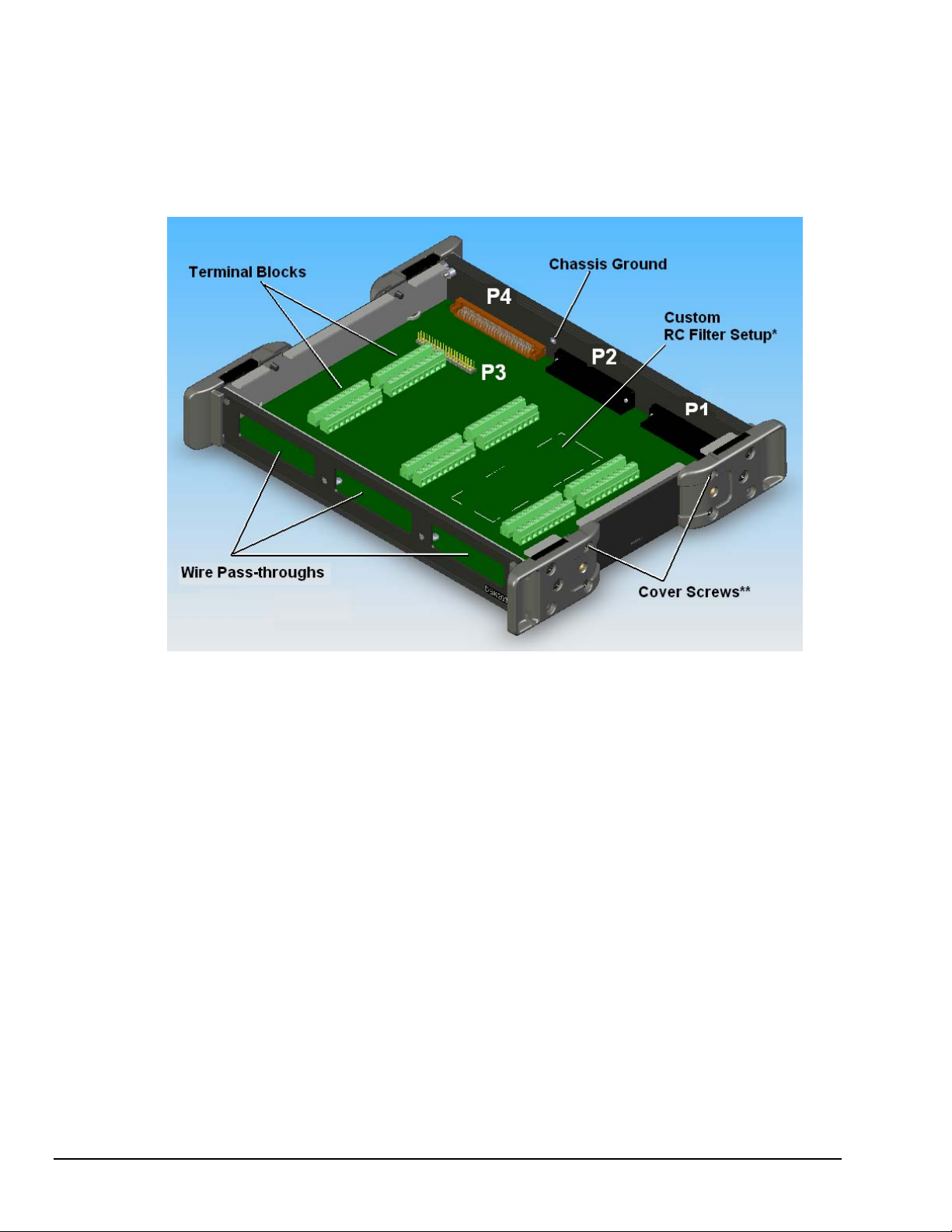
Overview
The various part numbers [DBK202, /203, /203A, /204, and /204c] of these closely related products are
described in the table on page 1. With exception of the DBK202 being a “board only,” the layout for each
is as indicated in the following figure.
DBK203A, Cover Plate Removed
* Custom RC Filter Setup is discussed in the section entitled, Adding Resistor/Cap acitor Filter
Networks, page 12.
** To remove the cover plate, remove the upper inside screw from each of the corner mounting
brackets (often referred to as protective ears); then lift the plate from the unit.
The information included in this section, when combined with that found in related DBK card and DBK
module sub-sections should enable you to set up your desired configuration.
It is important to note that the DaqBoard/2000 Series boards communicate [external from the host PC]
through a 100-pin P4 connector. The P1, P2, and P3 connectors discussed in association with these boards
are subset connectors of the 100-pin P4 connector. Certain DaqBook/2000 Series devices have both a P4
connector and a set of P1, P2, and P3 connectors on the unit. The System Connections and Pinouts chapter
includes pinouts for both types of devices, i.e., boards and “books.”
Each of the adapters discussed in this section provide a DB37 P1 connector, DB37 P2 connector, and a
40-pin “on-board” P3 header.
o P1 is used for Analog Input
o P2 for Digital I/O
o P3 for Pulse/Frequency (Digital and Counter/Timer) I/O
o P4 includes all signals found in P1, P2, and P3
In addition to these four connectors, each device includes terminal blocks designated TB1 through TB12.
The screw terminal blocks tie-in to P1, P2, and P3 and provide for easy signal connection.
pg. 2, DBK202, DBK203, and DBK204 Series
938994 DBK Option Cards and Modules
Page 3
Screw-Terminal Adapter Board
The DBK202 Board provides a means of connecting channel input signals to a /2000 Series device through
one of three methods:
• With cables connected to P1, P2, and P3 connectors, as applicable.
• With signal wires connected to the appropriate screw-terminal blocks (TB1 through TB12).
Note that the DBK202 board’s silkscreen clearly identifies all screw terminals.
• With a combination of the above two methods.
When connecting a DBK202 to a P4 connector, a CA-195 cable is used. The cable has a P4 connector
located at each end.
Note: DBK202 contains mounting holes that allow the board to be secured inside a user-provided
enclosure.
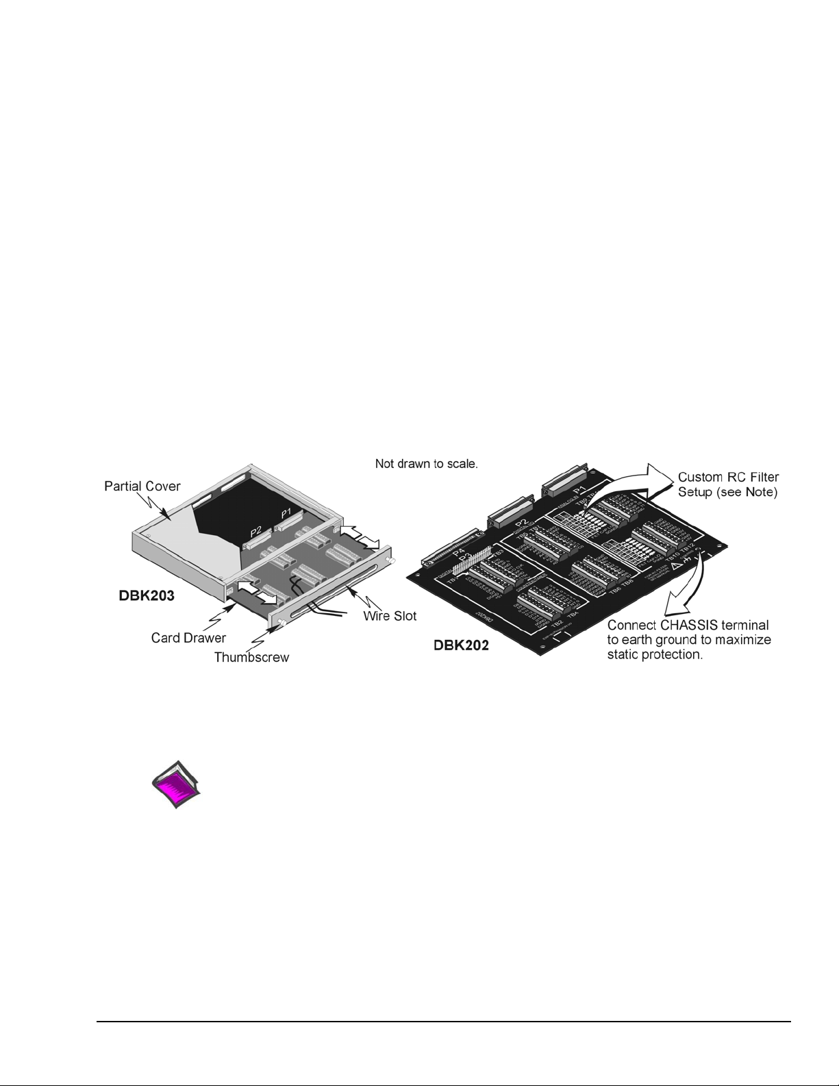
Screw-Terminal Adapter Modules
The DBK203, DBK203A, DBK204, and DBK204c each consist of a DBK202 board housed in a chassis.
The DBK203 [and DBK204 and DBK204c units that use it] include a card drawer that can be slid free of
the module. The sliding card drawer provides easy access to the twelve terminal blocks and to the 40-pin
P3 header. The DBK203A (which supersedes the DBK203) and the DBK204 and DBK204c units which
use the DBK203A have no slide out drawer.
DBK203 Includes a Slide-Out DBK202 Board
DBK203A has no Slide-Out Option
Reference Note for Custom RC Filter Setup:
You can install resistors and capacitors to create RC networks for P1 Analog Input Channels.
For detailed information, refer to Adding Resistor/Capacitor Filter Networks, which begins on
page 12 of this DBK section.
DBK Option Cards and Modules 938994 DBK202, DBK203, and DBK204 Series, pg. 3
Page 4
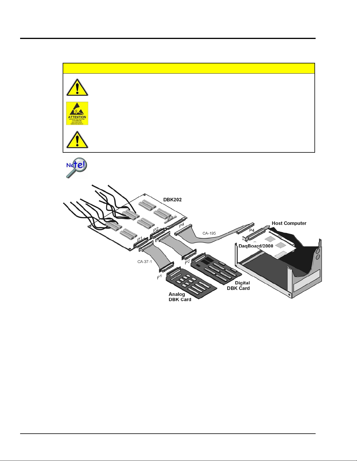
Connection Tips
CAUTION
Turn off power to the host PC and externally connected equipment prior to connecting
cables or signal lines to the DBK. Electric shock or damage to equipment can result
even under low-voltage conditions.
Take ESD precautions (packaging, proper handling, grounded wrist strap, etc.)
Use care to avoid touching board surfaces and onboard components. Only handle
boards by their edges (or ORBs, if applicable). Ensure boards do not come into
contact with foreign elements such as oils, water, and industrial particulate.
Do not confuse connectors. Ensure that you only connect P1 I/Os to P1, P2 I/Os to P2,
and P3 I/Os to P3. Improper connection may result in equipment damage.
Be sure to align the P4 orientation indicators () prior to mating the P4 connectors.
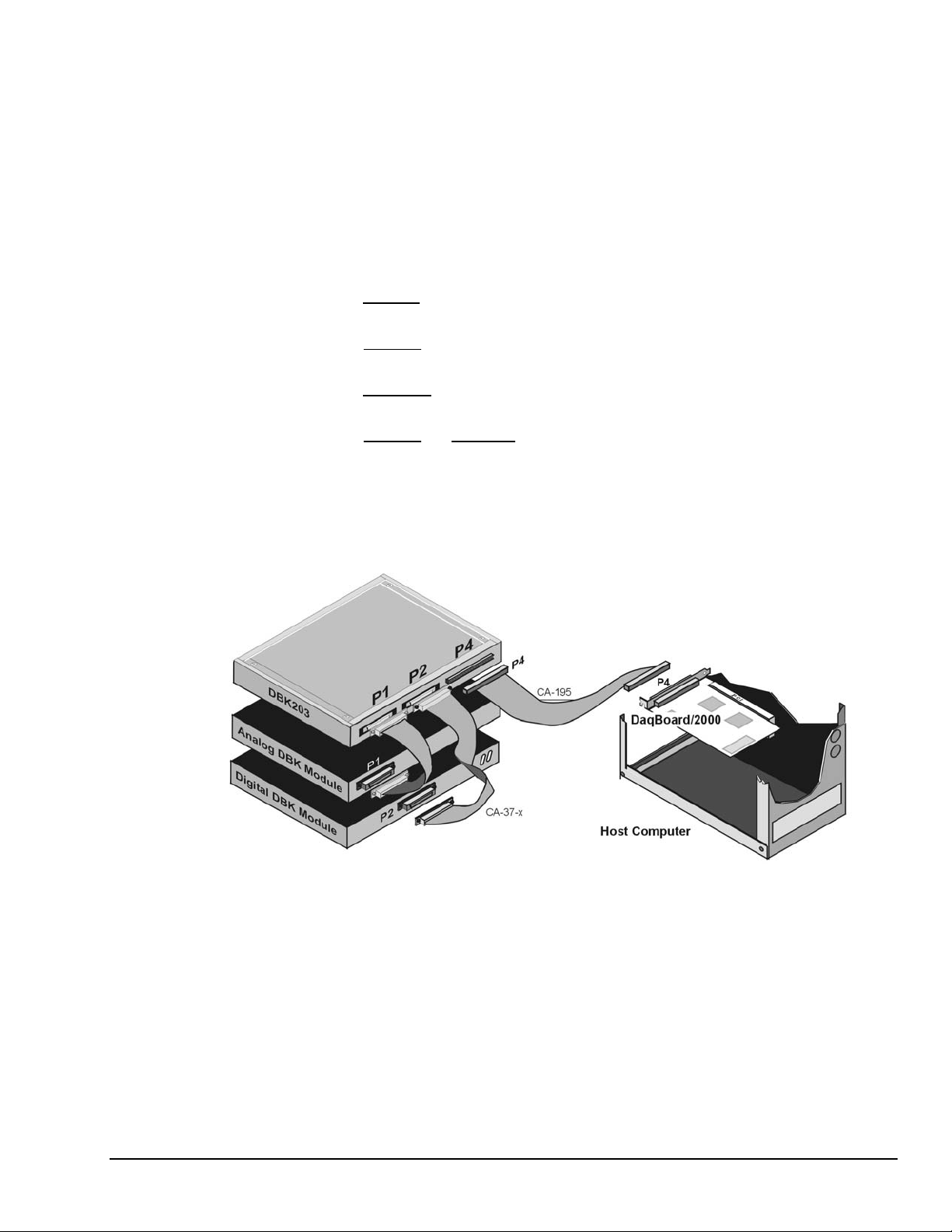
Example of a DBK202 Connected to Analog and Digital DBK Cards via P1 and P2, Respectively
The illustrations and actual board silkscreen are the only references you should need to make proper
connections.
A list of connection tips follows:
1. Ensure power is removed from the device(s) to be connected.
2. Observe ESD precautions when handling the board and making connections.
3. Do not make redundant connections. For example, for ANALOG IN you can use the P1
(DB37) connector or Terminal Blocks TB9 through TB12. You would not use both sets of
ANALOG IN connectors.
4. There is no need to access the board within a DBK203, DBK203A, DBK204, or DBK204c
unless you need to make connections to P3 or to a terminal block.
pg. 4, DBK202, DBK203, and DBK204 Series
938994 DBK Option Cards and Modules
Page 5
5. The board’s 100-pin P4 connector connects to the DaqBoard/2000 P4 connector via a
CA-195 Cable.
6. To obtain maximum protection from static, connect the CHASSIS terminal to earth ground.
Notes: Regarding connections to DB37 connectors and to the P3 (40-pin) header:
(a) P1 connects to an analog DBK card or module’s P1 connector via a CA-37 cable.
(b) P2 connects to a Digital DBK card or module’s P2 connector via a CA-37 cable.
(c) The 40-pin header (P3) connects to a Pulse/Frequency DBK card, or to a module’s
P3 connector via a CA-60 cable. Note that CA-60 cables have a 40-pin female
connector at one end and a DB37 (37-pin) male connector at the other end.
7. To access the board, i.e., to connect to P3 or to terminal blocks:
DBK202 – access of the board is direct, or as determined by your own custom
a)
enclosure.
b)
DBK203 – Loosen the two thumbscrews on the front panel and slide the card
drawer free of the unit.
c)
DBK203A – Remove the upper inside screw from each of the four corner brackets
(see figure, page 2) and lift the cover plate from the unit.
d)
DBK204 and DBK204c – Follow step 2b or 2c as applicable to your unit.
8. For DBK204 and DBK204c refer to the separate CE Cable Kit instructions that are included
with the associated CE cable kit.
Example of a DaqBoard/2000 System using a DBK203 (or DBK203A)
DBK Option Cards and Modules 938994 DBK202, DBK203, and DBK204 Series, pg. 5
Page 6

Using Screw-Terminal Blocks
Turn off power to the host PC and externally connected equipment prior to connecting cables or
signal lines to the DBK. Electric shock or damage to equipment can result even under low-voltage
conditions.
Take ESD precautions (packaging, proper handling, grounded wrist strap, etc.)
Use care to avoid touching board surfaces and onboard components. Only handle boards by their
edges (or ORBs, if applicable). Ensure boards do not come into contact with foreign elements
such as oils, water, and industrial particulate.
Do not confuse connectors. Ensure that you only connect P1 I/Os to P1, P2 I/Os to P2, and P3
I/Os to P3. Improper connection may result in equipment damage.
Be sure to align the P4 orientation indicators () prior to mating the P4 connectors.
CAUTION
1. Review the preceding CAUTIONS and the P4 alignment note.
2. Access the terminal blocks:
DBK202 – access of the board is direct, or as determined by your own custom
a)
enclosure.
b)
DBK203 – Loosen the two thumbscrews on the front panel and slide the card
drawer free of the unit.
c)
DBK203A – Remove the upper inside screw from each of the four corner brackets
(see figure, page 2) and lift the cover plate from the unit.
d)
DBK204 and DBK204c – Follow step 2b or 2c as applicable to your unit.
3. Make the wiring connections to the terminals. Refer to the board’s silkscreen and to the pin
correlations on the next few pages.
4. Tighten the terminal block screws snug. Do not over-tighten.
In general, the following terminal block-to-signal relationships apply:
o TB9, TB10, TB11, and TB12 are used for ANALOG IN and provide a connection
option to the P1 (DB37) connector.
o TB5, TB6, TB7, and TB8 are used for DIGITAL I/O and provide a connection
option to the P2 (DB37) connector.
o TB1, TB2, TB3, and TB4 are used for Pulse/Frequency/Digital I/O and provide a
connection to the 40-pin header (P3).
pg. 6, DBK202, DBK203, and DBK204 Series
938994 DBK Option Cards and Modules
Page 7

P3 40-pin
Header
The following pages correlate the DBK202 terminal block connectors with the associated pins of
the P1, P2, and P3 DB37 connectors. Note that the System Connections and Pinouts chapter
contains additional pin-outs, and includes references to the 100-pin P4 connector.
P4 (100 pins) P2 (37-pins) P1 (37-pins)
DBK202 Board
DBK Option Cards and Modules 938994 DBK202, DBK203, and DBK204 Series, pg. 7
Page 8

Correlation to P1 – Pertains to Terminal Blocks TB9, TB10, TB11, and TB12 for Analog I/O.
TB9 P1 Pin Number and Description (see Note 1)
DIFF SE
0H 0 37 CH 0 IN (Single-Ended Mode) / CH 0 HI IN (Differential Mode)
0L 8 18 CH 8 IN (Single-Ended Mode) / CH 0 LO IN (Differential Mode)
1H 1 36 CH 1 IN (Single-Ended Mode) / CH 1 HI IN (Differential Mode)
1L 9 17 CH 9 IN (Single-Ended Mode) / CH 1 LO IN (Differential Mode)
2H 2 35 CH 2 IN (Single-Ended Mode) / CH 2 HI IN (Differential Mode)
2L 10 16 CH 10 IN (Single-Ended Mode) / CH 2 LO IN (Differential Mode)
3H 3 34 CH 3 IN (Single-Ended Mode) / CH 3 HI IN (Differential Mode)
3L 11 15 CH 11 IN (Single-Ended Mode) / CH 3 LO IN (Differential Mode)
FILT CAP LO N/A For RC filter networks install a wire jumper between the relevant FILT CAP LO and
SGND 19 Signal Ground, Sense Common; reference ground, not for general use.
TB10 P1 Pin Number and Description (see Note 1)
DIFF SE
4H 4 33 CH 4 IN (Single-Ended Mode) / CH 4 HI IN (Differential Mode)
4L 12 14 CH 12 IN (Single-Ended Mode) / CH 4 LO IN (Differential Mode)
5H 5 32 CH 5 IN (Single-Ended Mode) / CH 5 HI IN (Differential Mode)
5L 13 13 CH 13 IN (Single-Ended Mode) / CH 5 LO IN (Differential Mode)
6H 6 31 CH 6 IN (Single-Ended Mode) / CH 6 HI IN (Differential Mode)
6L 14 12 CH 14 IN (Single-Ended Mode) / CH 6 LO IN (Differential Mode)
7H 7 30 CH 7 IN (Single-Ended Mode) / CH 7 HI IN (Differential Mode)
7L 15 11 CH 15 IN (Single-Ended Mode) / CH 7 LO IN (Differential Mode)
FILT CAP LO N/A For RC filter networks install a wire jumper between the relevant FILT CAP LO and
SGND 19 Signal Ground, Sense Common; reference ground, not for general use.
TB11 P1 Pin Number and Description
TTL TRIG 25 TTL Trigger, Digital IN, External TTL Trigger Input
A/I CLK 20 A/I Clock, External ADC Pacer Clock Input/ Internal ADC Pacer Clock Output
EXP 5 5 Expansion 5. Digital OUT, external GAIN select bit 1
EXP 6 6 Expansion 6. Digital OUT, external GAIN select bit 0
EXP 7 3 Expansion 7. Digital OUT, external ADDRESS, select bit 3
EXP 8 22 Expansion 8. Digital OUT, external ADDRESS, select bit 2
EXP 9 4 Expansion 9. Digital OUT, external ADDRESS, select bit 1
EXP 10 23 Expansion 10. Digital OUT, external ADDRESS, select bit 0
EXP 11 26 Expansion 11. Simultaneous Sample and Hold (SSH)
AGND * Analog Ground, Common
TB12 P1 Pin Number and Description
AGND * Analog Ground, Common
AGND * Analog Ground, Common
AGND * Analog Ground, Common
AGND * Analog Ground, Common
AGND * Analog Ground, Common
AGND * Analog Ground, Common
+ 15 V 21 Expansion, +15 V Power
- 15 V 2 Expansion, -15 V Power
AGND * Common Ground
+ 5 V 1 Expansion, +5 V Power
*Refer to Ground Correlation Tables in the System Connections and Pinouts chapter.
AGND. Note that there is no association between FILT CAP LO and P4.
AGND. Note that there is no association between FILT CAP LO and P4.
P1 – TB9
P1 – TB10
P1 – TB11
P1 – TB12
Note 1: For TB9 and TB10, the filter network portion of the silk screen is not shown. Instead, the DIFF and SE channel
identifiers have been moved next to the screws for ease in identification.
pg. 8, DBK202, DBK203, and DBK204 Series
938994 DBK Option Cards and Modules
Page 9

Correlation to P2 – Pertains to Terminal Blocks TB5, TB6, TB7, and TB8 for Digital I/O.
TB5 P2 Pin Number and Description
DGND * Digital Ground, Common
DGND * Digital Ground, Common
A7 30 Digital I/O: P2, Digital Port A, Bit 7; or P2 Expansion Data Bit 15
A6 31 Digital I/O: P2, Digital Port A, Bit 6; or P2 Expansion Data Bit 14
A5 32 Digital I/O: P2, Digital Port A, Bit 5; or P2 Expansion Data Bit 13
A4 33 Digital I/O: P2, Digital Port A, Bit 4; or P2 Expansion Data Bit 12
A3 34 Digital I/O: P2, Digital Port A, Bit 3; or P2 Expansion Data Bit 11
A2 35 Digital I/O: P2, Digital Port A, Bit 2; or P2 Expansion Data Bit 10
A1 36 Digital I/O: P2, Digital Port A, Bit 1; or P2 Expansion Data Bit 9
A0 37 Digital I/O: P2, Digital Port A, Bit 0; or P2 Expansion Data Bit 8
TB6 P2 Pin Number and Description
+5 V 18 Expansion +5 V Power
+5 V 20 Expansion +5 V Power
DGND * Digital Ground, Common
DGND * Digital Ground, Common
DGND * Digital Ground, Common
DGND * Digital Ground, Common
DGND * Digital Ground, Common
DGND * Digital Ground, Common
DGND * Digital Ground, Common
DGND * Digital Ground, Common
TB7 P2 Pin Number and Description
DGND * Digital Ground, Common
DGND * Digital Ground, Common
C7 22 Digital I/O: P2, Digital Port C, Bit 7; or P2 Expansion Data Bit 7
C6 23 Digital I/O: P2, Digital Port C, Bit 6; or P2 Expansion Data Bit 6
C5 24 Digital I/O: P2, Digital Port C, Bit 5; or P2 Expansion Data Bit 5
C4 25 Digital I/O: P2, Digital Port C, Bit 4; or P2 Expansion Data Bit 4
C3 26 Digital I/O: P2, Digital Port C, Bit 3; or P2 Expansion Data Bit 3
C2 27 Digital I/O: P2, Digital Port C, Bit 2; or P2 Expansion Data Bit 2
C1 28 Digital I/O: P2, Digital Port C, Bit 1; or P2 Expansion Data Bit 1
C0 29 Digital I/O: P2, Digital Port C, Bit 0; or P2 Expansion Data Bit 0
TB8 P2 Pin Number and Description
DGND * Digital Ground, Common
DGND * Digital Ground, Common
B0 10 Digital I/O: P2, Digital Port B, Bit 0; or P2 Expansion READ Output
B1 9 Digital I/O: P2, Digital Port B, Bit 1; or P2 Expansion WRITE Output
B2 8 Digital I/O: P2, Digital Port B, Bit 2; or P2 Expansion RESET Output
B3 7 Digital I/O: P2, Digital Port B, Bit 3; or P2 Expansion Address Bit 4 Out
B4 6 Digital I/O: P2, Digital Port B, Bit 4; or P2 Expansion Address Bit 3 Out
B5 5 Digital I/O: P2, Digital Port B, Bit 5; or P2 Expansion Address Bit 2 Out
B6 4 Digital I/O: P2, Digital Port B, Bit 6; or P2 Expansion Address Bit 1 Out
B7 3 Digital I/O: P2, Digital Port B, Bit 7; or P2 Expansion Address Bit 0 Out
* Refer to Ground Correlation Tables in the System Connections and Pinouts chapter.
P2 – TB5
P2 – TB6
P2 – TB7
P2 – TB8
DBK Option Cards and Modules 938994 DBK202, DBK203, and DBK204 Series, pg. 9
Page 10

Correlation to P3 – Pertains to Terminal Blocks TB1, TB2, TB3, and TB4 for Pulse/Frequency/Digital I/O.
TB1 P3 Pin Number and Description
D0 10 P3 Digital Port Bit 0
D1 9 P3 Digital Port Bit 1
D2 8 P3 Digital Port Bit 2
D3 7 P3 Digital Port Bit 3
D4 6 P3 Digital Port Bit 4
D5 5 P3 Digital Port Bit 5
D6 4 P3 Digital Port Bit 6
D7 3 P3 Digital Port Bit 7
DGND * Digital Ground, Common
+5V 20 Expansion, +5 Volt Power
TB2 P3 Pin Number and Description
D8 29 P3 Digital Port Bit 8
D9 28 P3 Digital Port Bit 9
D10 27 P3 Digital Port Bit 10
D11 26 P3 Digital Port Bit 11
D12 25 P3 Digital Port Bit 12
D13 24 P3 Digital Port Bit 13
D14 23 P3 Digital Port Bit 14
D15 22 P3 Digital Port Bit 15
DGND * Digital Ground, Common
DGND * Digital Ground, Common
TB3 P3 Pin Number and Description
CH0 (DAC0) 34 Analog Out; Analog DAC 0 Output
AGND * Analog Ground, Common; intended for use with DACs
EXP 0 (DAC2) 32 Analog Out; Analog DAC 2 Output
AGND * Analog Ground, Common; intended for use with DACs
CH1 (DAC1) 33 Analog Out; Analog DAC 1 Output
A/O CLK 21 Analog Out Clock; External DAC Pacer Clock Input/
Internal DAC Pacer Clock Output
EXP 1 (DAC3) 31 Analog Out; Analog DAC 3 Output
DGND * Digital Ground, Common
+15 V 19 Expansion, + 15 VDC
-15 V 37 Expansion, -15 VDC
TB4 P3 Pin Number and Description
EXP 2 12 Reserved
EXP 3 13 Reserved
EXP 4 14 Reserved
TMR 0 15 P3 Timer 0 Output
TMR 1 16 P3, Timer 1 Output
CNT 3 35 P3 Counter 3 Input
CNT 2 17 P3 Counter 2 Input
CNT 1 36 P3 Counter 1 Input
CNT0 18 P3 Counter 0 Input
DGND * Digital Ground, Common
* Refer to Ground Correlation Tables in the System Connections and Pinouts chapter.
P3 – TB1
P3 – TB2
P3 – TB3
P3 – TB4
pg. 10, DBK202, DBK203, and DBK204 Series
938994 DBK Option Cards and Modules
Page 11

Using the P3 Header
Disconnect the DBK202, DBK203, DBK203A, DBK204, or DBK204c from power and
from signal sources prior to connecting the CA-60 cable to the 40-pin header.
Take ESD precautions (packaging, proper handling, grounded wrist strap, etc.)
Use care to avoid touching board surfaces and onboard components. Only handle
boards by their edges (or ORBs, if applicable). Ensure boards do not come into
contact with foreign elements such as oils, water, and industrial particulate.
Do not confuse connectors. Ensure that you only connect P1 I/Os to P1, P2 I/Os to P2,
and P3 I/Os to P3. Improper connection may result in equipment damage.
CAUTION
P3 40-Pin Header
If you need a DB37 connector
for P3, connect a CA-60 cable
to this 40-pin header.
The P3 Corner Section of a DBK202
The P3 40-pin header can be used to obtain a DB37 type connector via a CA-60 cable.
To make a DB37 connector available for P3:
1. Follow the preceding CAUTIONS and ensure power is removed from the system devices.
2. Access the terminal blocks:
DBK202 – access of the board is direct, or as determined by your own custom
a)
enclosure.
b)
DBK203 – Loosen the two thumbscrews on the front panel and slide the card
drawer free of the unit.
c)
DBK203A – Remove the upper inside screw from each of the four corner brackets
(see figure, page 2) and lift the cover plate from the unit.
d)
DBK204 and DBK204c – Follow step 2b or 2c as applicable to your unit.
3. Connect the CA-60 cable to the 40-pin header.
4. Return the system to normal operation.
Reference Note:
There is no direct pin-to-pin correlation between the pins on the header and those on the
DB37 connector. For P3 pinout information refer to chapter 2, System Connections and
Pinouts.
DBK Option Cards and Modules 938994 DBK202, DBK203, and DBK204 Series, pg. 11
Page 12

Adding Resistor/Capacitor Filter Networks
WARNING
Disconnect the DBK202, DBK203, DBK203A, DBK204, or DBK204c from power and
from signal sources prior to installing capacitors or resistors.
Ensure wire strands do not short power supply connections (+15 V, -15 V, +5 V, etc.) to
any terminal potential. Failure to do so could result in damage to DaqBook/2000 Series
devices, DaqBoard/2000 Series boards, or DaqBoard/2000c Series boards.
Do not exceed maximum allowable inputs (as listed in product specifications). There
should never be more than 30 V with reference to analog ground (AGND) or earth
ground.
Do not operate DBK202 on an exposed metal surface.
You must provide strain-relief (lead slack) to all leads leaving DBK202, /203, /203A,
/204, or /204c. Use tie-wraps [not included] to secure strain-relief.
Always connect the CHASSIS terminal to earth ground. This will maximize static
protection.
CAUTION
You can install customized RC filter networks to improve the signal-to noise ratio when an unacceptable
level of noise exists. DBK202, /203, /203A, /204, and /204c include sockets for installing RC filter
networks directly on the board.
The following table contains values that are typical for RC filter network components.
Typical One-Pole Low Pass Filter Values
for DBK202, DBK203, DBK203A, DBK204, and DBK204c
R C f f
Ohms µF Hertz (-3dB) kHz (-3dB)
510 1 312 0.31
510 0.47 664 0.66
510 0.22 1419 1.42
510 0.1 3122 3.12
510 0.047 6643 6.64
510 0.022 14192 14.19
510 0.01 31223 31.22
510 0.0047 66431 66.43
470 0.0033 102666 102.67
pg. 12, DBK202, DBK203, and DBK204 Series
938994 DBK Option Cards and Modules
Page 13

An Example of Customer-Installed Capacitors and Filters for RC Networks on a DBK202
Prior to installing RC components, review the previous WARNING and CAUTION statements; then read
over the following information regarding resistors and capacitors.
• Do not use RC filters in conjunction with additional DBK expansion accessories.
• Prior to installing a resistor to the filter network you must drill a 1/16” hole through
the center pinhole [beneath the board’s silkscreen resistor symbol] as indicated in the
above figure. Failure to do so will short-circuit the resistor.
• Do not drill holes on the board for channels, unless those channels are to receive a
filter network (see preceding statement).
• Resistors should be ¼ watt, film-type with up to 5% tolerance. Do not use wire-
wound resistor types.
• A resistor value of 510 Ω is recommended. Do not exceed 510 Ω.
• Capacitors used are to be of the film dielectric type (e.g., polycarbonate or
NPO ceramic), above 0.001 µF.
• RECOMMENDED: For reduction of both Common Mode Noise and Differential
Mode Noise, use one capacitor between Channel High and AGND; and use a second
capacitor between Channel Low and AGND.
• For reduction of Differential Noise [when no reduction of Common Mode Noise is
needed] position a capacitor across the respective Channel High and Channel Low.
• When in Differential Mode, using capacitors between Channel High, Channel Low,
and AGND may cause a slight degradation of wideband Common Mode rejection.
• When making a RC filter network, always install a wire jumper between the relevant
FILT CAP LO and AGND. FILT CAP LO terminals are located on TB9 and TB10.
DBK Option Cards and Modules 938994 DBK202, DBK203, and DBK204 Series, pg. 13
Page 14

pg. 14, DBK202, DBK203, and DBK204 Series
938994 DBK Option Cards and Modules
 Loading...