

Page 1

DAC488
User's Manual
12-Bit Digital-to-Analog Converter Systems; Models DAC488/2 and DAC488/4
the smart approach to instrumentation ™
IOtech, Inc.
25971 Cannon Road
Cleveland, OH 44146-1833
Phone: (440) 439-4091
Fax: (440) 439-4093
E-mail: sales@iotech.com
Internet: www.iotech.com
i
DAC488
12-Bit Digital-to-Analog Converter Systems
Models DAC488/2 and DAC488/4
Released Per EO#1927R11
© 1998 by IOtech, Inc. June 1998 Printed in the United Stat es of America.
User's Manual
107-0901
p/n
Rev.
1.0
Page 2
Warranty
Your IOtech warranty is as stated on the product warranty card. You may contact IOtech by phone, fax
machine, or e-mail in regard to warranty-related issues.
Phone: (440) 439-4091, fax: (440) 439-4093, e-mail: sales@iotech.com
Limitation of Liability
IOtech, Inc. cannot be held liable for any damages resulting from the use or misuse of this product.
Copyright, Trademark, and Licensing Notice
All IOtech documentation, software, and hardware are copyright with all rights reserved. No part of this
product may be copied, reproduced or transmitted by any mechanical, photographic, electronic, or other
method without IOtech’s prior written consent. IOtech product names are trademarked; other product
names, as applicable, are trademarks of their respective holders. All supplied IOtech software (including
miscellaneous support files, drivers, and sample programs) may only be used on one installation. You may
make archival backup copies.
FCC Statement
IOtech devices emit radio frequency energy in levels compliant with Federal Communications Commission
rules (Part 15) for Class A devices. If necessary, refer to the FCC booklet How To Identify and Resolve
Radio-TV Interference Problems (stock # 004-000-00345-4) which is available from the U.S. Government
Printing Office, Washington, D.C. 20402.
CE Notice
Many IOtech products carry the CE marker indicating they comply with the safety and emissions
standards of the European Community. As applicable, we ship these products with a Declaration of
Conformity stating which specifications and operating conditions apply.
Warnings and Cautions
Refer all service to qualified personnel. This caution symbol warns of possible personal injury or
equipment damage under noted conditions. Follow all safety standards of professional practice and the
recommendations in this manual. Using this equipment in ways other than described in this manual can
present serious safety hazards or cause equipment damage.
This warning symbol is used in this manual or on the equipment to warn of possible injury or death
from electrical shock under noted conditions.
This ESD caution symbol urges proper handling of equipment or components sensitive to damage from
electrostatic discharge. Proper handling guidelines include the use of grounded anti-static mats and
wrist straps, ESD-protective bags and cartons, and related procedures.
Calibration Notice
As applicable, IOtech calibrates its hardware products to published specifications. Periodic hardware
calibration is not covered under the warranty and must be performed by qualified personnel as specified in
this manual. Improper calibration procedures may void the warranty.
Quality Notice
IOtech has maintained ISO 9001 certification since 1996. Prior to shipment, we thoroughly test our
products and review our documentation to assure the highest quality in all aspects. In a spirit of
continuous improvement, IOtech welcomes your suggest i ons.
Page 3
Introduction to this Manual
This manual covers the setup and operation of the DAC488/4 and the DAC488/2 digital-to-analog converter
systems. This manual is organized as follows:
• Chapter 1 - DAC488 Overview gives an overview of the basic features of a DAC488 system. DAC488
accessories and specifications are also provided.
• Chapter 2 - DAC488 Setup explains in detail the various hardware features of the DAC488 unit.
• Chapter 3 - DAC488 Power & Assembly provides detailed instructions on line-voltage selection and
fuse replacement, rack-mount and bench-top installation, as well as power-up activation.
• Chapter 4 - DAC488 Operation explains the DAC488 theory of operation. Descriptions of the
DAC488 command groups, triggering, internal buffer, control modes, as well as IEEE 488 bus support,
are provided.
• Chapter 5 - IEEE 488 Background describes the history and the basic concepts of IEEE 488
operation, including the various IEEE 488 bus commands and bus lines.
• Chapter 6 - DAC488 Calibration explains the manual and automatic procedures for calibrating the
DAC488 unit.
• Chapter 7 - DAC488 Commands discusses the entire command set covering the DAC488/4 and
DAC488/2 units. The command syntax, groups, and reference are provided. The description format of
the individual commands includes the command type, syntax, description, and an example program
excerpt.
• Chapter 8 - Troubleshooting provides a reference for possible solutions to technical problems. Before
calling for technical assistance, refer to this chapter.
•
The Appendix provides background information concerning the IEEE 488 bus, the serial bus, and
ASCII controls.
• The Index provides a comprehensive alphabetical listing of the main terms and topics in this manual.
Also, the Abbreviations on the last pages of this manual, provides an overall list of abbreviations,
including acronyms and ASCII control codes, as an additional reference for this manual and for other
related literature.
CAUTION
CAUTION
CAUTIONCAUTION
Using this equipment in ways other than described in this manual can cause personal
injury or equipment damage. Before setting up and using your equipment, you should
read all documentation that covers your system. Pay special attention to cautions and
warnings formatted like this one.
DAC488 User’s Manual i
Page 4

Table of Contents
1 - DAC488 Overview
Introduction…… 1
Accessories…… 2
Specifications…… 2
Digital I/O…… 2
Analog Output…… 3
IEEE 488…… 3
General…… 4
2 - DAC488 Setup
The Package…… 5
Hardware Setup…… 6
Front & Rear Panel Layouts…… 6
Default Settings…… 7
IEEE 488 Bus Address Selection…… 7
Mode Selection…… 7
Analog Output Ports…… 7
Digital I/O Port…… 8
Transistor-Transistor Logic (TTL) Lev el s…… 9
High Voltage/High Current Digital Outputs…… 9
External Trigger/SRQ Input…… 11
To Configure the Digital Output Lines…… 11
3 - DAC488 Power & Assembly
Introduction…… 13
Internal Components…… 13
Factory Service…… 13
Power Line & Fuse Configuration…… 14
Line Voltage Selection…… 14
To Select the Line Voltage…… 15
Fuse Replacement…… 16
To Replace the Fuse…… 16
Rack-Mount & Bench-Top Assembly…… 17
Rack Mount…… 17
Bench Top…… 17
Power-Up & Performance Tests…… 18
Power-Up Activation…… 18
Programming Examples……19
KYBDCTRL.BAS Program…… 19
To Run the Keyboard Controller Program…… 19
DAC488 Command Responses…… 20
Performance Verification…… 20
To Verify the Port Volt age - 10-V ol t Range…… 21
To Verify the Port Voltage - 5-Volt Range…… 21
To Verify the Port Voltage - 1-Volt Range…… 22
Data Transfer Speeds…… 22
4 - DAC488 Operation
Introduction…… 23
Command Groups…… 23
System & Port Commands…… 23
Command Support…… 24
Port Triggering…… 24
Trigger Processing & Trigger Overrun…… 25
Internal Buffer…… 26
Buffer Data…… 26
Buffer Save-and-Restore Program…… 27
Control Modes…… 28
Direct Control Mode…… 28
Indirect Control Mode……28
Stepped Control Mode…… 28
Waveform Control Mode…… 29
Multiple Port Synchronization…… 30
Synchronized Waveforms Program…… 30
Digital I/O Port…… 32
User-Defined System Defaults…… 33
IEEE 488 Bus Support…… 33
Bus Lines…… 33
Bus Commands…… 34
Bus Addresses…… 34
Bus Terminators…… 34
5 - IEEE 488 Background
History…… 35
General Bus Structure…… 35
Bus Lines & Bus Commands…… 36
Bus Management Lines…… 36
Handshake Lines…… 37
Data Transfer Lines…… 37
Bus Command Groups…… 38
More On Service Requests…… 39
6 - DAC488 Calibration
Introduction…… 41
Calibration Procedures…… 41
Manual Calibration Procedure…… 42
Part I: Connections & Preparations…… 42
Part II: Acquiring the Gain Calibration
Constants…… 42
Part III: Acqui ri ng t he Offset Calibration
Constant…… 43
BASIC Calibration Program…… 43
Automatic Calibration Procedure…… 47
Part I: Connections & Preparations…… 47
Part II: Automatic Calibration Process…… 48
Part III: Automatic Cal i bration Report…… 49
ii DAC488 User’s Manual
Page 5

7 - DAC488 Commands
A - Appendix
Introduction…… 51
Command Syntax…… 51
Command Groups…… 53
System Commands…… 53
Port Commands…… 53
Command Support……53
Command Summary…… 54
Command Reference…… 57
@ - Trigger On Command…… 58
A - Autorange…… 59
B - Buffer Data…… 60
C - Control Mode…… 61
D - Digital Output…… 63
E? - Query Error Status…… 64
F - Buffer Definition…… 66
G - GET Trigger Mask…… 67
H - Offset Calibration…… 68
I - Interval…… 69
J - Gain Calibration…… 70
K - End-Or-Identify Control…… 71
L - Buffer Location…… 72
M - Service Request Mask…… 73
N - Number of Cycles…… 74
O - Output Format…… 75
P - Port Select…… 76
Q - External Trigger Mask…… 77
R - Range Select…… 78
S - System Defaults…… 79
T - Command Trigger Mask…… 80
U - User Status…… 81
V - Value Output…… 84
W - Test…… 85
X - Execute…… 86
Y - Bus Terminator…… 87
? - Query…… 88
Serial Poll Status Byte…… 89
IEEE 488 Bus & Serial Bus Lines…… 93
IEEE 488 Bus Commands…… 94
ASCII Codes…… 95
ASCII Code Summary…… 95
Decimal Values 00 to 63 - ACG, UCG & LAG……
95
Decimal Values 64 to 127 - TAG & SCG…… 96
ASCII Code Details…… 97
Decimal Values 00 to 31 - ACG & UCG
Characteristics…… 97
Decimal Values 00 to 31 - ACG & UCG
Descriptions…… 98
Decimal Values 32 to 63 - LAG…… 99
Decimal Values 64 to 95 - TAG…… 100
Decimal Values 96 to 127 - SCG…… 101
Index…… 103
Abbreviations…… 106
8 - Troubleshooting
Radio Interference Problems…… 91
Electrostatic Discharge (ESD) Damage…… 91
Other Issues…… 91
Power-Up Activation…… 91
Trigger Processing & Trigger Overrun…… 92
Query Error Status…… 92
DAC488 User’s Manual iii
Page 6

−
Notes
iv DAC488 User’s Manual
Page 7

DAC488 Overview 1
Introduction…… 1
Accessories…… 2
Specifications…… 2
Digital I/O…… 2
Analog Output…… 3
IEEE 488…… 3
General…… 4
Introduction
The DAC488 is a multiple output Digital-to-Analog Converter (DAC) interface for the IEEE 488 bus. Each
port uses a 12-bit plus-sign D/A converter and is isolated from IEEE common and the other ports by up to
500 volts. Each port can be programmed for full-scale output of ±1 volt, ±5 volts and ±10 volts. Voltage
values may be specified in volts or bits in increments of 1 part in 4096 plus-sign. The resolution of the
ranges is 250 µVolts, 1.25 mVolts and 2.5 mVolts respectively.
Four operational modes are available to allow each port to be controlled directly from the IEEE bus or in an
automatic manner. An internal 8,191 sample buffer is included which can be loaded with waveform
voltages. These voltages may then be output in sequence either on a periodic interval or in a triggered
fashion. The DAC488 sample buffer is automatically saved in Non-Volatile RAM (NV-RAM) as it is
loaded, allowing a once only configuration of the device for many applications. All configuration settings
may also be saved in Non-Volatile RAM for use as the permanent defaults.
Each of the ports can be triggered from three different sources: An external trigger, a trigger command, or a
Group Execute Trigger (
trigger sources may be selected for each port.
GET) bus command. Since each port can be triggered independently, different
The interface also provides 8 TTL level digital inputs and 8 digital outputs. The digital outputs may be
internally configured as either TTL level or 100 mA outputs to allow interfacing with solenoids, relays or
other devices. An external trigger/SRQ input is also provided which can trigger the interface or generate an
SRQ on either a falling or rising edge of a TTL compatible signal. All digital signals as well as +5 Volts
and ground are accessible via a 20-pin card edge connector (Standard version) or a DB25 pin connector
(CE version) located on the rear panel.
Calibration may be done automatically by connecting the interface to a Keithley Model 199 DMM. No
mechanical adjustments are required. After calibration, a complete calibration report will be printed if the
interface is connected to an IEEE printer.
Throughout this manual, the term “DAC488” refers to either a DAC488/4 or a DAC488/2.
DAC488 User’s Manual DAC488 Overview 1
Page 8
Accessories
Additional accessories that can be ordered for the DAC488 include:
• CA-1: Power Cable
• CA-7-1: 1.5 foot IEEE 488 Cable
• CA-7-3: 6 foot shielded IEEE 488 Cable
• CA-7-4: 6 foot reverse entry IEEE 488 Cable
• CA-8-20: 6 foot, 20 conductor ribbon cable with a card edge connector on one end, the other end
• CA-35-2: 2 foot, DB25 male-to-female pin Connector
• CA-35-6: 6 foot, DB25 male-to-female pin Connector
• CN-40-12: DAC488 Analog Output Connector
• CN-6-20: 20-pin card edge Connector.
• CN-20: Right Angle IEEE 488 adapter, male and female
• CN-22: IEEE 488 multi-tap bus strip, four female connectors in parallel
• CN-23: IEEE 488 panel mount feed-through connector, male and female
Specifications
unterminated.
Please read this manual carefully! If equipment is used in any manner not specified in
this manual, the protection provided by the equipment may be impaired.
CAUTION
CAUTION
CAUTIONCAUTION
Digital I/O
WARNING
WARNING
WARNINGWARNING
Do not use the DAC488 unit outdoors! This unit is intended for indoor use only!
Unexpected outdoor conditions could result in equipment failure, bodily injury or
death!
Terminal Installation Category: Standard: Not Applicable. CE: Category 1.
Transistor-Transist or Logic (TTL) Leve ls: Digital outputs will drive 2 TTL loads or sink 100mA
(selectable using internal configuration jumper).
Digital Inputs and Digital Outputs: 8 inputs, TTL level compatible; 8 outputs, internally selectable TTL
level compatible or open collector with 100 mA @ 50 V drive capability.
Service Request/External Trigger Input: 1 line, TTL level compatible.
Connectors: Standard: One 20-pin card edge connector. CE: One DB25 (25-pin) connector.
2 DAC488 Overview DAC488 User’s Manual
Page 9
Analog Output
Terminal Installation Category: Standard: Not Applicable. CE: Category 1.
DC Output Voltage and Resolution
DC Output Current and Output Resistance: 10 mA maximum; and <500 mΩ (typical)
Accuracy (25 ±±±± 5°°°°C; Iout = 1 mA):
Warm Up Time to Rated Accuracy: 1 hour
Temperature Coefficient (0°°°° to 20°°°° C, and 30°°°°to 50°°°° C): ±(0.002% of setting + 100 µV) / °C
Channel to Channel Isolation: Standard: 500 V max, 100,000 V-Hz.
Channel to Digital Low Isolation: Standard: 500 V max, 100,000 V-Hz.
Connectors: One 12-pin quick disconnect analog.
WARNING
WARNING
WARNINGWARNING
There may be up to 200 V isolation potential between analog common and earth (CE
version) or up to 500 V isolation potential (Standard version). Avoid contact with
analog output terminals and the cables connected to them. Do not apply power until
after the AC line and analog output connections have been properly made. The AC
line must remain connected to the unit whenever the analog output terminals are
connected to a device exceeding 60 VDC or 30 Vrms common mode voltage. Contact
with voltage potentia ls could cause bodily injury or death!
CAUTION
CAUTION
CAUTIONCAUTION
Solid wire is recommended for the analog output terminal connections. If stranded
wire is used, then strip the wire 6 mm, and twist or tin the stripped end. After
tightening the connector, check that no loose wire strands are present.
1V Range: ± 1.02375 V, 250 µV/bit
5V Range: ± 5.11875 V, 1.25 mV/bit
10V Range: ± 10.2375 V, 2.5 mV/bit.
1V Range: ±(0.05% of setting + 1 mV)
5V Range: ±(0.05% of setting + 3 mV)
10V Range: ±(0.05% of setting + 10 mV)
CE: 200 volts max, 100,000 V-Hz
CE: (Channel Common to Earth) 200 V max, 100,000 V-Hz
IEEE 488
CAUTION
CAUTION
CAUTIONCAUTION
The IEEE 488 terminal must only be used to control a non-isolated IEEE 488 system.
The common mode voltage (cable shell to earth) must be zero.
Terminal Installation Category: Standard: Not Applicable. CE: Category 1.
Implementation: SH1, AH1, T4, TE0, L4, LE0, SR1, RL0, PP0, DC1, DT1,E1.
Terminators: Programmable CR, LF, LF CR and CR LF with EOI.
Programmable: IEEE Bus Terminators, EOI Control, SRQ Mask, Port Voltage, Gain, Offset, Digital I/O
lines, Output Format, Internal Buffer, Mode.
Connector: Standard IEEE 488 connector with metric studs.
DAC488 User’s Manual DAC488 Overview 3
Page 10
General
WARNING
WARNING
WARNINGWARNING
Service: This product contains no operator serviceable parts. Fuse replacement and
the changing of selected line voltage must be performed by qualified service personnel.
Never open the DAC488 case while it is connected to the AC line, or when analog
output terminals are connected to a device exceeding 60 VDC or 30 Vrms common
mode voltage!
Terminal Installation Category: Standard: Not Applicable. CE: Category 2 for Line Voltage Input
terminal. All other terminals are Category 1.
Dimensions: 425 mm wide x 45 mm high x 309 mm deep (16.75" x 1.75" x 12")
Weight: 3.32 kg. (7.31 lbs)
Environment: Standard: Indoor use, 0° to 50°C; 0 to 95% RH (non-condensing).
CE: Indoor use at altitudes below 2000 meters, 0° to 40°C; 0 to 80% RH up to 31°C decreasing
linearly 4% RH/°C to 40°C.
Controls: Power Switch (external), line voltage selection switch (internal), mode and IEEE address DIP
switch (external), calibration enable switch (external), digital output port configuration jumper
(internal)
Indicators: LEDs for TALK, LISTEN, SRQ, ERROR, TEST and POWER
Power: Internally selectable 105-125 V or 210-250 V; 50-60 Hz, 35 VA Max
Fuse: 3/8A, Slo Blo, 3AG (for 105-125 V power line) or 3/4A, Slo Blo, 3AG (for 210-250 V power line)
CAUTION
CAUTION
CAUTIONCAUTION
Line Voltage: The protective conductor terminal on the AC line connector must be
connected to an external protective earthing system. Failure to make such a
connection will impair protection from shock. If common mode voltages connected to
the analog input terminals exceed 60 VDC or 30 Vrms, the AC line connector must
remain connected even when the unit is powered “off.” If it becomes necessary to
disconnect the AC line connector, you must first disconnect all power to the analog
input terminals.
CAUTION
CAUTION
CAUTIONCAUTION
Fuse Failure: Fuse failure indicates a possible problem within the device circuitry. If a
fuse blows, contact a qualified service representative. Replacement fuses are to be
installed by qualified service personnel with the unit disconnected from the power
source and with all other terminals disconnected. If the line voltage selector is
changed, then the fuse designated for that line voltage must be used.
4 DAC488 Overview DAC488 User’s Manual
Page 11

DAC488 Setup 2
The Package…… 5
Hardware Setup…… 6
Front & Rear Panel Layouts…… 6
Default Settings…… 7
IEEE 488 Bus Address Selection…… 7
Mode Selection…… 7
Analog Output Ports…… 7
Digital I/O Port…… 8
Transistor-Transistor Logic (TTL) Lev el s…… 9
High Voltage/High Current Digital Outputs…… 9
External Trigger/SRQ Input…… 11
To Configure the Digital Output Lines…… 11
The Package
All DAC488 components are carefully inspected prior to shipment. When you receive your digital-toanalog converter system, carefully unpack all items from the shipping carton and check for any damage
which may have occurred during shipment. Promptly report the damage to the shipping agent and your
sales representative. Retain all shipping materials in case you must return the unit to the factory.
Every DAC488 package includes the following items listed by part number:
• DAC488/2 or DAC488/4: Digital-to-Analog Converter with Digital I/O and IEEE 488
• WINDOWS PANELS: Programmed Disks in IBM format, including Installation Card and Licensing
Agreement (PR-10)
• 107-0901: DAC488 User’s Manual
• PR-2: Warranty Card
• DAC488-003: Accessories Kit for DAC488, which includes the following:
• CA-1: Power Cable
• CA-35-2 or CA-35-6: DB25 Male-to-Female Connector, 2 or 6 feet respectively (CE version)
• CN-6-20: 20-pin Card Ed ge Connector (S tandard version)
• CN-40-12: 12-pin Analog Output Connector
• FE-1: Rubber Feet (4)
• EN-6: Rack Ears (2)
• HA-41-6: Rack Screws (4)
• PR-9: Rack Mounting Instruct i ons
• FU-1-.375: 3/8A Replacement Fuse
• FU-1-.75: 3/4A Replacement Fuse
DAC488 User’s Manual DAC488 Setup 5
Page 12
Hardware Setup
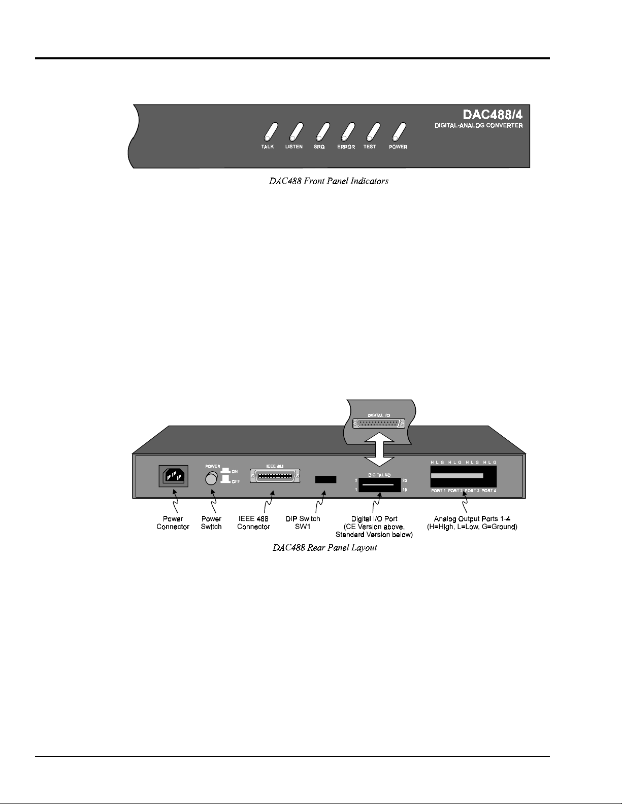
Front & Rear Panel Layouts
Six LED indicators on the DAC488 front panel, display the unit status. The following list describes the
functions of these indicators:
• TALK: ON when DAC488 is in the Talker state; OFF when in the Idle or Listener state.
• LISTEN: ON when DAC488 is in the Listener state; OFF when in the Idle or Talker state.
• SRQ: ON when DAC488 generated a service request; OFF when no SRQ is pending.
• ERROR: ON when an error has occurred; OFF when no error condition exists.
• TEST: ON when used in conjunction with the Test (
been established with the DAC488. The TEST LED will flash when the DAC488 is calibrating in the
auto-calibration mode. The TEST LED will then remain lit when finished calibrating in the autocalibration mode.
• POWER: ON when power is being applied while the power switch is in the ON position; OFF when
power is not present.
W) command to veri fy tha t communication has
6 DAC488 Setup DAC488 User’s Manual
Page 13
Default Settings
The DAC488 unit may be operated from either 110 VAC or 220 VAC.
The operating voltage is set by an internal switch. The factory set
operating voltage appears on the label placed over the power jack on the
rear panel . To change the operating vol t age, see section Line Voltage
Selection in Chapter 3.
The DAC488 unit has one 8-microswitch DIP switch (SW1) accessible
from the rear panel. This DIP switch determines the IEEE 488 bus
address and its operating mode. The switch is read only when the unit is
powered on and should be set prior to applying power. The figure
illustrates the factory default for the DIP microswitch settings. To
modify the default settings, disconnect the power cord from the AC line
and change the micros witch se ttings using a small screwdriver. The
enclosure does not need to be opened to change the DIP microswitch
settings.
IEEE 488 Bus Address Selection
The IEEE 488 bus address is set by positioning the
rear-panel DIP microswitches 1 through 5. T he
address can be set from 0 through 30 and is read
only at power on. The address is selected by
simple binary weighting with microswitch 1 being
the Least Significant Bit (LSB) and microswitch 5
the Most Significant Bit (MSB). The factory
default setting is address 9, as shown in the
diagram. If address 31 is selected, it defaults to
address 30 because the IEEE 488 standard has
reserved address 31.
Mode Selection
The DAC488 can be operated in one of two modes:
Normal operating mode or automatic calibration
mode, which are selected by the rear-panel DIP
microswitch 8. The factory default setting for
microswitch 8 is normal operating mode, as shown
in the diagram.
Analog Output Ports
The DAC488 can be considered as multiple
isolated IEEE 488 to Analog Converters. The unit
occupies one IEEE 488 bus address. Each port has
a low (L), high (H) , and ground (case ground) l ine.
The case ground line may be connected to the
shield of shielded cable if this type of cable is used
to carry the analog signals. The pinouts for all
analog ports are labeled on the rear panel of the
unit. Each analog output is capable of sourcing
and sinking a maximum current of 1 0 mA.
DAC488 User’s Manual DAC488 Setup 7
Page 14
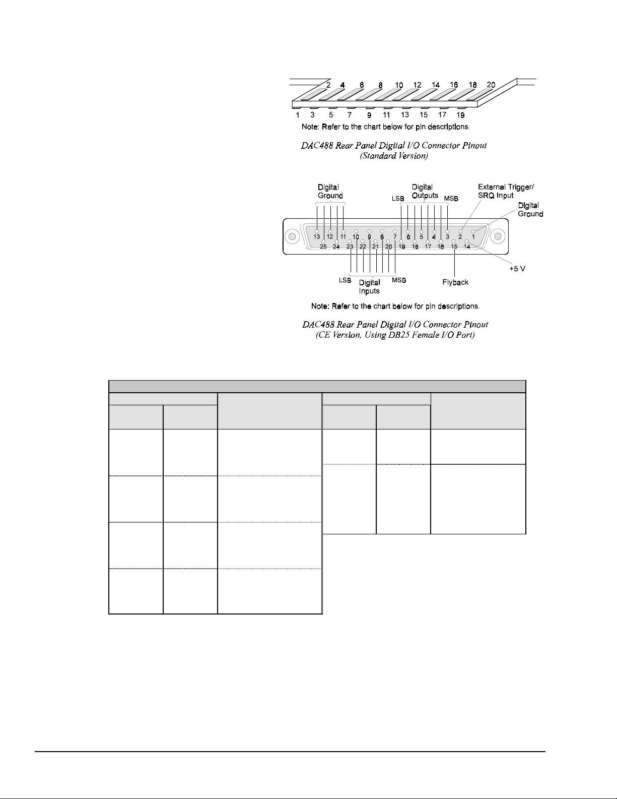
Digital I/O Port
The DAC488 has eight digital input
lines and eight digital output lines. At
power on, the configuration of digital
output lines is determined by the
options saved as the startup
configuration. In order to set the digital
output lines to a particular state upon
power on, the System Defaults (
command must be used after all the
lines have been configured. For
example, if it is desired to have digital
output line 1 set high and the other lines
set low at power on, the lines would be
set to this configuration using the
Digital Output (
configuration would be saved using the
System Defaults (
S
)
D) command. Then this
S
) co mmand.
Digital I/O Port Pinouts
Connector Pin Connector Pin
Standard
(20-pin)
1 23 Digital Input Bit 1 (LSB ) 17 15 Flyback
2 10 Digital Input Bit 2 18 2 Ext. Trigger/SRQ Input
3 22 Digital Input Bit 3 19 14
4 9 Digital Input Bit 4 1 Digital Ground
5 21 Digital Input Bit 5 11 Digital Ground
6 8 Digital Input Bit 6 12 Digital Ground
7 20 Digital Input Bit 7 13 Digital Ground
8 7 Digital Input Bit 8 (MSB) 24 Digital Ground
9 19 Digital Output Bit 1 (LSB )
10 6 Digital Output Bit 2
11 18 Digital Output Bit 3
12 5 Digital Output Bit 4
13 17 Digital Output Bit 5
14 4 Digital Output Bit 6
15 16 Digital Output Bit 7
16 3 Digital Output Bit 8 (MSB)
CE Version
(DB25)
Connector Pin
Description
Standard
(20-pin)
20
CE Version
(DB25)
+5 V (≤ 50 mA load)
25 Digital Ground
Connector Pin
Description
8 DAC488 Setup DAC488 User’s Manual
Page 15
Transistor-Transistor Logic (TTL) Levels
The digital output lines will drive 2 TTL loads. All digital input lines are less than 1.5 TTL loads. All
inputs are protected against damage due to high static voltages. Normal precautions should be taken to
limit the input voltages to the range of -0.3 to +7.0 volts. All I/O lines are referenced to Digital Ground
(Standard Version Pin 2 0, CE Version Pin 1).
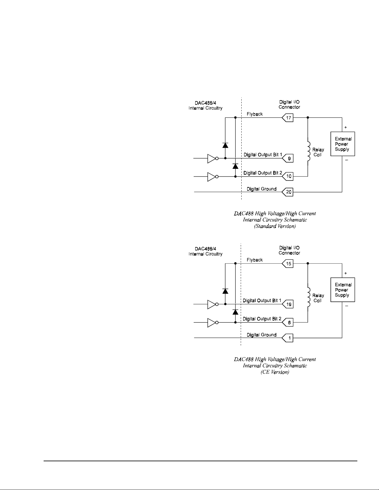
High Voltage/High Current Digital Outputs
In addition to interfacing with TTL
logic levels, the digital output lines
can be configured as high
voltage/high current outputs. These
outputs can sink up to 100 mA at 50
VDC through the use of open
collector drivers with integral diodes
for inductive load transient
suppression. This allows for
interfacing the digital outputs with
relays, lamps and solenoids.
As shown in the following
schematics, the gates driving the
digital outputs (when configured for
high voltage/high current operation)
contain internal diodes to suppress
inductive transients. The cathodes
of these diodes are tied together and
connected to the Flyback pin on the
digital I/O port. By connecting the
Flyback pin to the positive end of
the supply driving the relays, the
internal diodes will be connected in
parallel with the relay coils and thus
prevent inductive spikes from
damaging the internal circuitry of
the DAC488.
DAC488 User’s Manual DAC488 Setup 9
Page 16
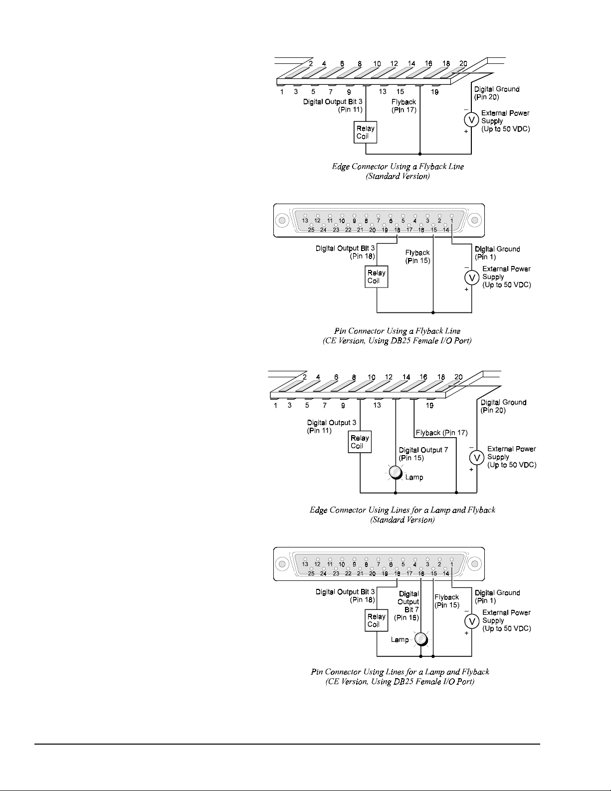
When used with relays or solenoids,
the Flyback pin on the edge card
connector should be connected to
the positive supply lead of the power
supply used with the external
devices being driven, as shown in
the following figures . To configure
the digital output lines for this
purpose, it is necessary to open the
enclosure and reposition the
configuration jumper. For
instructions on how this is done, see
section To Configure the Digital
Output Lines in the following text.
Once the digital output lines have
been configured for high level
operation, they can be used to drive
devices such as relays, solenoids and
displays. For example, a typical
application may require a lamp and
a relay to be driven by the Standard
version DAC488. For this example,
the relay is connected to digital
output pin 11 and the lamp is
connected to digital output pin 15,
as shown in the following diagram.
Using this same example for the CE
version DAC488, the relay is
connected to digital output pin 18
and the lamp is connected to digital
output pin 16, also shown in the next
diagram.
Since a relay is used for this
application, the Flyback terminal is
connected to the positive terminal of
the external power supply. Note
also that the Ground lead of the
power supply should be connected
to pin 20 (Digital Ground) on the
Standard card edge connector, or to
pin 1 (Digital Ground) on the CE
pin connector.
10 DAC488 Setup DAC488 User’s Manual
Page 17
External Trigger/SRQ Input
The External Trigger/SRQ input (Standard pin 18; CE pin 2) can be used to trigger the DAC488 once it has
been properly armed. The DAC488 can be programmed to trigger on a positive-going or negative-going
edge by using the External Trigger Mask (
pulse. A trigger pulse may also be used to generate an SRQ by using the Service Request Mask (
command. The maximum rate at which the DAC488 can be triggered is 1 trigger pulse every 1 millisecond.
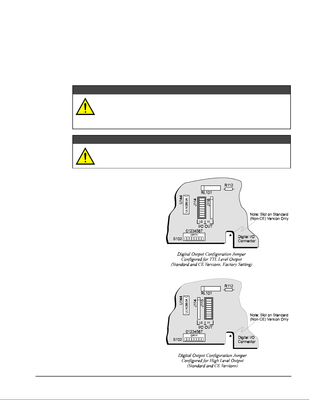
To Configure the Digital Output Lines
Service: This product contains no operator serviceable parts. Fuse replacement and
the changing of selected line voltage must be performed by qualified service personnel.
Never open the DAC488 case while it is connected to the AC line, or when analog
output terminals are connected to a device exceeding 60 VDC or 30 Vrms common
mode voltage!
Do not connect external high level devices to the digital output lines unless they have
first been configured for this purpose. Otherwise the interface may be damaged.
1. First, disconnect any cables from the
analog output terminals. Next,
disconnect the power cord from the
AC line and from the interface. Then
disconnect any other cables prior to
disassembly.
Q) command. Any TTL leve l signal may be used as a trigger
WARNING
WARNING
WARNINGWARNING
CAUTION
CAUTION
CAUTIONCAUTION
M)
2. Place the interface on a flat surface.
Remove the six screws on top of the
case and remove the top cover.
3. Located in front of the rear-panel DIP
switch (SW1) are three sockets and a
configuration jumper. This jumper is
factory set to configure the digital
output lines for low level TTL logic
levels, as shown in the figure.
4. To configure the digital output lines
as high voltage/high c urrent outputs,
first remove the configuration jumper.
5. Next, reinsert it so that the center
socket is now connected to the right
socket, as shown in the second figure.
6. Once the jumper has been
repositioned for your particular
application, make note of the new
setting for later reference.
7. Carefully reassemble the unit.
DAC488 User’s Manual DAC488 Setup 11
Page 18

−
Notes
12 DAC488 Setup DAC488 User’s Manual
Page 19

DAC488 Power & Assembly 3
Introduction…… 13
Internal Components…… 13
Factory Service…… 13
Power Line & Fuse Configuration…… 14
Line Voltage Selection…… 14
To Select the Line Voltage…… 15
Fuse Replacement…… 16
To Replace the Fuse…… 16
Rack-Mount & Bench-Top Assembly…… 17
Rack Mount…… 17
Bench Top…… 17
Power-Up & Performance Tests…… 18
Power-Up Activation…… 18
Programming Examples……19
KYBDCTRL.BAS Program…… 19
To Run the Keyboard Controller Program…… 19
DAC488 Command Responses…… 20
Performance Verification…… 20
To Verify the Port Voltage - 10-Volt Range…… 21
To Verify the Port Voltage - 5-Volt Range…… 21
To Verify the Port Voltage - 1-Volt Range…… 22
Data Transfer Speeds…… 22
Introduction
Internal Components
The heart of the DAC488 is a 6809 microprocessor [U101] supported by 16K bytes of firmware EPROM
[U102] and 32K bytes of battery-backed-up RAM [U103]. Interface to the IEEE 488 bus is accomplished
by a 9914 interface chip [U105]. A 65C22 [U109] generates real-time interrupts for the firmware operating
system and also drives the front panel LED indicators.
Isolation of the analog ports is accomplished using separate bipolar power supplies for each port. OptoIsolators are used to isolate the digital and analog circuitry. High voltage/high current output capability is
available on the digital o ut put port thr ough a 74HCTLS240 and a ULN2803A peripheral driver [U144].
Calibration of the analog ports through p rogram control is accomplished by the use of two 8-bit D/A
converters on each analog circuit. One converter is used to adjust the gain and the other converter to adjust
the offset.
Factory Service
Chapter 8 provides a troubleshooting reference for possible solutions to technical problems. Before calling
for technical assistance, refer to this chapter.
However, if problems in using the DAC488 still persist, you should contact the factory. Many problems
can be resolved by discussing the problems with the appropriate applications department. If the problem
cannot be solved by this method, you will be instructed as to the proper return procedure.
DAC488 User’s Manual DAC488 Power & Assembly 13
Page 20
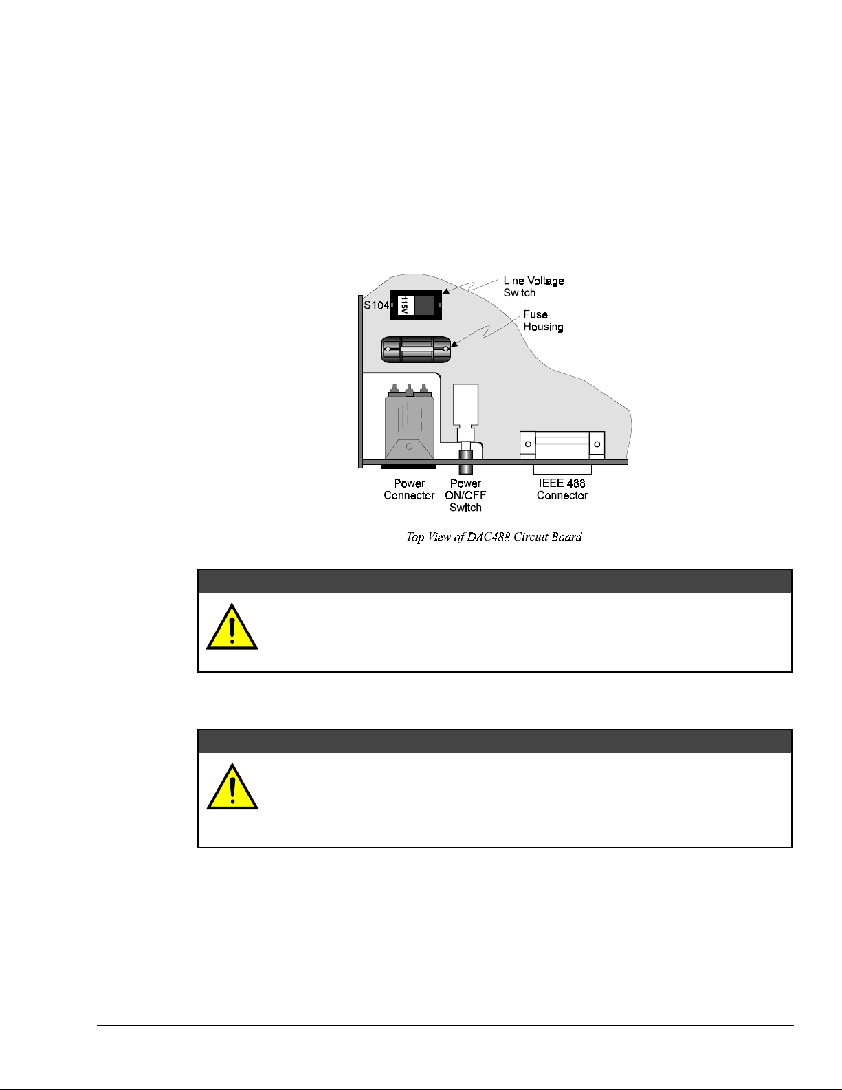
Power Line & Fuse Configuration
The power configuration of the DAC488 unit consists of selecting the line voltage and replacing the fuses.
Each DAC488 unit has a factory default to operate at 105-125 volts AC. However, each unit may be
operated at either 105-125 or 210-250 VAC.
Do not use the DAC488 unit outdoors! The unit is intended for indoor use only!
Outdoor conditions could result in equipment failure, bodily injury or death!
Never disassemble the DAC488 case while it is connected to the AC power line, or
when analog output terminals are connected to a device exceeding 60 VDC or 30 Vrms
common mode voltage! Internal voltage potentials exist which could cause bodily
injury or death!
To change the operating voltage of the DAC488 unit, it is necessary to open the enclosure. However,
before modifying the voltage, disconnect any input or output connections from the rear panel of the affected
unit and then disconnect the power cord from the power line terminal.
Line voltage must be set for 105-125 or 210-250 VAC to match the power being supplied to the DAC488
unit. If the line voltage is changed, the fuse must also be changed. Refer to the following text for the line
voltage switch and fuse locations.
WARNING
WARNING
WARNINGWARNING
WARNING
WARNING
WARNINGWARNING
Line Voltage Selection
As already mentioned, the DAC488 may be operated with 105-125 or 210-250 VAC, 50-60 Hz power, as
set by its internal line-voltage switch (labelled S104). Each unit is shipped from the factory with this
operating voltage setting marked on its rear panel. If this is not the appropriate power setting to be supplied
to the unit, then the line voltage and power fuse must be changed to avoid damage to the unit. The linevoltage selection procedure is outlined in the following steps.
CAUTION
CAUTION
CAUTIONCAUTION
Service: This product contains no operator serviceable parts, or operator replaceable
parts within the case. Fuse replacement and the changing of selected line voltage must
be performed by qualified service personnel. Never open the DAC488 case while it is
connected to the AC line, or when analog output terminals are connected to a device
exceeding 60 VDC or 30 Vrms common mode voltage. Contact with voltage potentials
could cause bodily injury or death!
14 DAC488 Power & Assembly DAC488 User’s Manual
Page 21
Note: If disassembly or disconnections are necessary, first turn off the power, then disconnect the analog
output cables, next disconnect the AC power line, and then any other cables, prior to disassembly.
To Select the Line Voltage
1. Turn off the power, then disconnect the analog output cables. Next, disconnect the AC power line
cord, and then all other test cables from the unit.
2. Place the unit on a flat surface. Remove the six screws on top of the case and remove the top cover.
3. Located next to the main power supply transformer is the line voltage selection switch (labelled S104).
Using a small screwdriver, insert the tip of the screwdriver into the slot of the switch and slide the
switch to the left or right until it "clicks" into place with the desired line voltage selection visible.
CAUTION
CAUTION
CAUTIONCAUTION
It is possible to place the line voltage switch (S104) in a partial position which could
cause equipment damage or malfunction. When changing the position of the line
voltage selection switch (S104), make sure the switch is completely positioned to the
115 V or 220 V selection. The switch will “click” into place when properly positioned.
4. Install a power line fuse appropriate for the line voltage. See section Fuse Replacement – Step 3,
following this section.
CAUTION
CAUTION
CAUTIONCAUTION
Fuse Failure: Fuse failure indicates a possible problem within the device circuitry. If a
fuse blows, contact a qualified service representative. Replacement fuses are to be
installed by qualified service personnel with the unit disconnected from the power
source and with all other terminals disconnected. If the line voltage selector is
changed, then the fuse designated for that line voltage must be used.
5. Make note of the new voltage setting for later reference.
6. Carefully reassemble the unit.
Note: For re-assembly, first reconnect the AC power line, next reconnect the analog output terminals, and
then any other cables, prior to reapplying power to the entire system.
DAC488 User’s Manual DAC488 Power & Assembly 15
Page 22
Fuse Replacement
The DAC488 unit contains an internal AC line fuse. The fuse is located next to the internal line-voltage
switch (S104). You may replace the fuse by using the procedures found in the following text.
Note: If disassembly or disconnections are necessary, first turn off the power, then disconnect the analog
To Replace the Fuse
1. Turn off the power, then disconnect the analog output cables. Next, disconnect the AC power line
cord, and then all other cables from the unit.
2. Place the unit on a flat surface. Remove the six screws on top of the case and remove the top cover.
3. Located next to the line-voltage selection switch (labelled S104) is the power fuse. Gently pull upward
on the plastic fuse housing. The entire housing with the fuse inside should be removed.
4. Open the fuse housing by pushing up on the tab on the bottom of the housing. Remove the fuse, and
replace it with the proper type using the following list as a guide:
CAUTION
CAUTION
CAUTIONCAUTION
Service: This product contains no operator serviceable parts, or operator replaceable
parts within the case. Fuse replacement and the changing of selected line voltage must
be performed by qualified service personnel. Never open the DAC488 case while it is
connected to the AC line, or when analog output terminals are connected to a device
exceeding 60 VDC or 30 Vrms common mode voltage. Contact with voltage potentials
could cause bodily injury or death!
output cables, next disconnect the AC power line, and then any other cables, prior to disassembly.
• For line voltage 105-125 V, use fuse type 3/4 A, Slo Blo, 3AG
• For line voltage 210-250 V, use fuse type 3/8 A, Slo Blo, 3AG
CAUTION
CAUTION
CAUTIONCAUTION
Fuse Failure: Fuse failure indicates a possible problem within the device circuitry. If a
fuse blows, contact a qualified service representative. Replacement fuses are to be
installed by qualified service personnel with the unit disconnected from the power
source and with all other terminals disconnected. If the line voltage selector is
changed, then the fuse designated for that line voltage must be used.
5. Close the housing. Insert the fuse into the fuse holder.
6. Make note of the new fuse rating for lat er reference. If you have also changed the operating linevoltage selection, return to the previous section Line Voltage Selection – Step 5.
7. Carefully reassemble the unit.
Note: For re-assembly, first reconnect the AC power line, next reconnect the analog output terminals, and
then any other cables, prior to reapplying power to the entire system.
16 DAC488 Power & Assembly DAC488 User’s Manual
Page 23
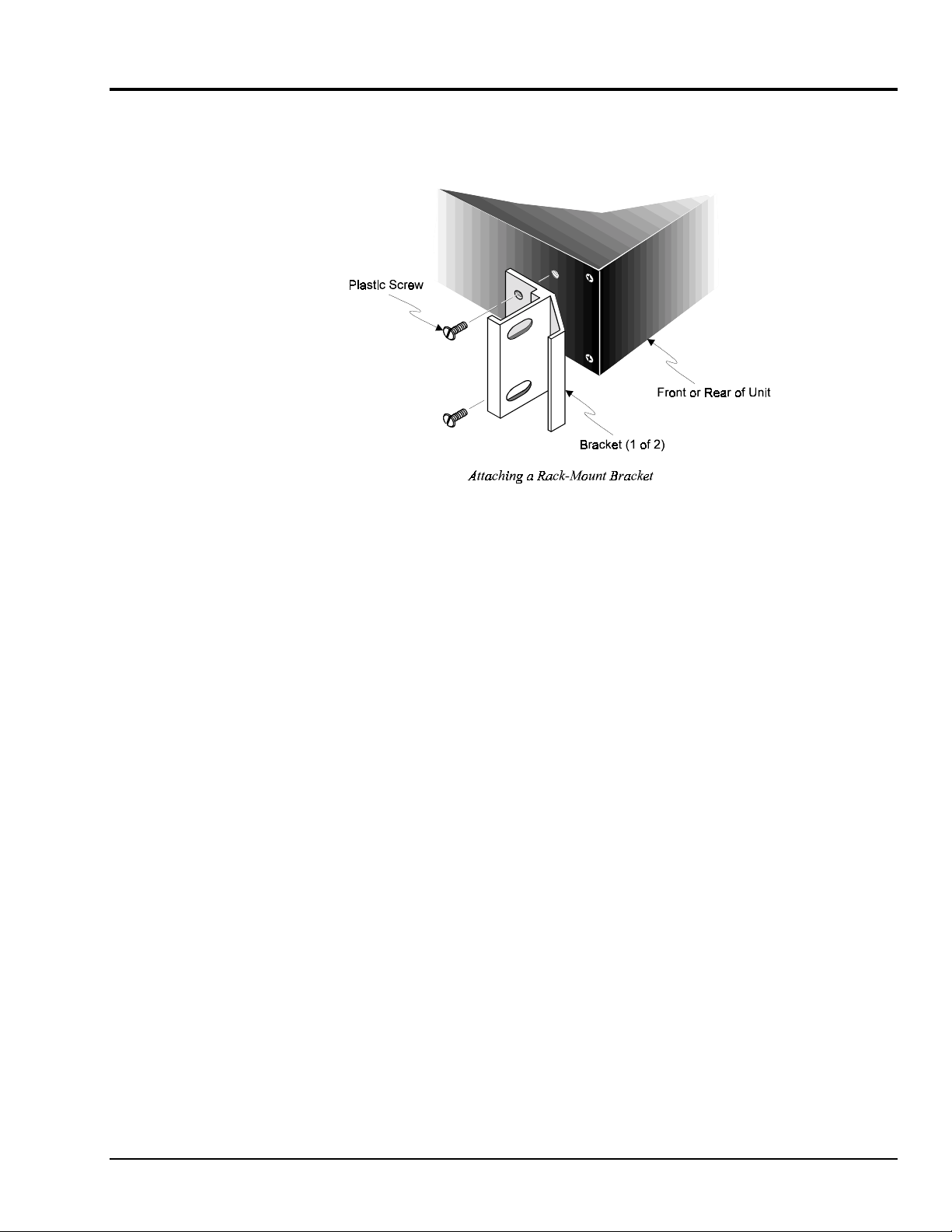
Rack-Mount & Bench-Top Assembly
The DAC488 includes accessories for rack-mount or bench-top assembly.
Rack Mount
If rack-mount assembly is required, remove the two plastic screws from the pre-drilled holes on each side of
the unit. Since the unit can be mounted with the front or rear panel facing the front of the rack fixture,
remove only those screws from the set of holes that will be toward the front of the rack. Attach the two rack
ears using the enclosed screws.
Bench Top
If bench-top assembly is required, install the self-adhesive rubber feet on the bottom of the unit
approximately one inch from each corner.
DAC488 User’s Manual DAC488 Power & Assembly 17
Page 24
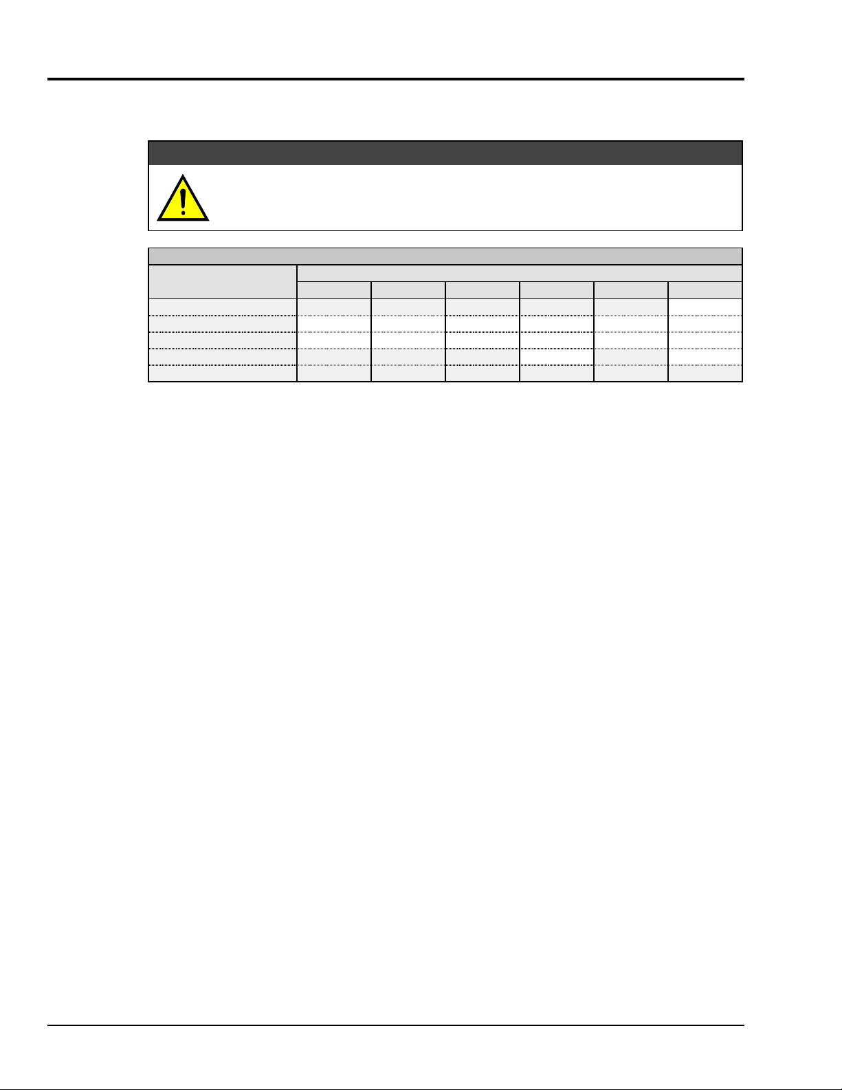
Power-Up & Performance Tests
Power-Up Activation
Line Voltage: The protective conductor terminal on the AC line connector must be
connected to an external protective earthing system. Failure to make such a
connection will impair protection from shock.
Condition
Normal (No Errors)
ROM Error
RAM Error
NV-RAM Checksum Error
No Power
With the power c ord plugged i n and connected to the DAC488, turn on the unit by depressing the rear-panel
power switch. All of the front-panel LED indicators should light up for approximately one second while the
DAC488 performs an internal ROM and RAM self-check. At the end of this self-check all of the LED
indicators should turn off except for POWER.
Otherwise, the DAC488 may be in an error condition according to the one of the four following LED
patterns:
TALK LISTEN SRQ ERROR TEST POWER
(Off) (Off) (Off) (Off) (Off) ON
ON ON ON ON ON ON
FLASHINGFLASHINGFLASHINGFLASHINGFLASHING ON
(Off) (Off) (Off) ON (Off) ON
(Off) (Off) (Off) (Off) (Off) (Off)
CAUTION
CAUTION
CAUTIONCAUTION
LED Patterns for Error Conditions
LED Indicators
• If all of the LED indicators remain on: T hen a ROM error has occurred.
• If the POWER LED indicator remains on while the rest of the LED indicators flash continuously:
Then a RAM error has occurred. Try cycling the power to the DAC488 to determine that the error is
repeatable.
• If the POWER and ERROR LED indicator remain on while the rest of the LED indicators are off:
Then a checksum error on Non-Volatile RAM occurred, and the saved configurations may be lost. The
checksum error condition may be cleared by doing a save of a configuration using the System Defaults
(
S) command. The error condition may also be cleared by using the Query Error Status (E?)
command.
• If all of the LED indicators are off: Then there may not be any power being supplied to the DAC488.
In this event, check to make sure that the AC power cable is securely connected at both ends.
Otherwise, there may be a problem with the fuse. For more information, see section Power Line &
Fuse Configuration earlier in this chapter.
18 DAC488 Power & Assembly DAC488 User’s Manual
Page 25

Programming Examples
The DAC488 programming examples use the Personal488 PC/IEEE 488 controller interface and the BASIC
Keyboard Controller (KBC) program. This KBC program
listed below.
KYBDCTRL.BAS Program
10 ' Personal488 Keyboard Controller Program
20 '
30 ' For use with the IOtech Personal488
40 ' IEEE 488 interface
50 '
100 OPEN "\DEV\IEEEOUT" FOR OUTPUT AS #1
110 IOCTL#1,"BREAK"
120 PRINT#1,"RESET"
130 OPEN "\DEV\IEEEIN" FOR INPUT AS #2
140 '
150 ON ERROR GOTO 300
160 PRINT#1,"ERROR OFF"
170 '
180 LINE INPUT "CMD> ",CMD$
190 PRINT#1,CMD$
200 '
210 IF IOCTL$(2)<>"1" THEN 180
220 PRINT INPUT$(1,2);
230 GOTO 210
290 '
300 ' Error Handler
310 '
320 IOCTL#1,"BREAK"
330 PRINT#1,"STATUS"
340 INPUT#2,ST$
350 PRINT CHR$(7);"Error #";MID$(ST$,15,2);": ";MID$(ST$,27)
360 RESUME NEXT
KYBDCTRL.BAS is included on the disk and is
The Keyboard Controller (KBC) program allows direct communication with the DAC488 (or any IEEE 488
device on the bus) via the keyboard, and displays any responses on the screen. This program is a
convenient method of exercising the DAC488 and becoming familiar with the commands and their actions.
To Run the Keyboard Controller Program
1. First, set the rear-panel DIP switch for bus address 9.
2. Connect an IEEE 488 cable from the IEEE 488 connector on the DAC488 to the IEEE 488 connector
on the Personal488 PC/IEEE 488 controller interface card.
3. Turn on the DAC488 by depressing the rear-panel power switch.
4. From the MS-DOS prompt on your computer screen, run the Keyboard Controller Program
KYBDCTRL.BAS and verify that the CMD> prompt appears on the screen.
DAC488 User’s Manual DAC488 Power & Assembly 19
Page 26

DAC488 Command Responses
(1)
(2)
(3)
(4)
(5)
(6)
(7)
(8)
CMD>
CMD>OUTPUT 09;W1X
CMD>OUTPUT 09;W0X
CMD>ENTER 09
A1 C0 P1 R0 V+00.00000
CMD>OUTPUT 09;P1 C0 A0 R3 V5.678
CMD>ENTER 09
A0 C0 P1 R3 V+05.67750
CMD>OUTPUT 09;P1 C0 A0 R3 V4.321
CMD>ENTER 09
A0 C0 P2 R2 V+04.32000
The above is a listing of the commands given to the DAC488 and the response received. Some commands
and command responses are separated by extra vertical and horizo ntal spaces for clarity although these
spaces will not actually appear when using the program. These eight command responses are explained as
follows:
• Line 1: Initial command prompt from the Keyboard Controller program.
• Line 2: Instruct the DAC488 to turn on its TEST LED indicator. The TEST LED indicator should light
up.
• Line 3: Instruct the DAC488 to turn off its TEST LED indicator. The TEST LED indicator should turn
off.
• Line 4: Retrieve the DAC488 default status: Autorange on, Direct control mode, Port 1 selected,
Ground range , and 0.0 volts.
• Line 5: Program the DAC488 Port 1 for 5.678 volts. A digital multimeter (DMM) connected to Port 1
should read 5.677 volts (± 10 mV) after this command string is executed.
• Line 6: Retrieve the DAC488 status: The programmed 5.678 volts was rounded to 5.67750 volts.
• Line 7: Program the DAC488 Port 2 for 4.321 volts. A digital multimeter (DMM) connected to Port 2
should read 4.320 volts (± 10 mV) after this command string is executed.
• Line 8: Retrieve the DAC488 status: The programmed 4.321 volts was rounded to 4.32000 volts.
Performance Verification
To verify that each DAC488 port is functioning within the specifications, the following procedure may be
used. If the port voltage is measured using a Keithley 199 DMM/Scanner, the reading should fall between
the low and high limits listed in the tables. The procedure is given for Port 1 although each port may be
tested by the Port Select (
DMM/Scanner using the calibration cable described in Chapter 6.
P
) command. It is assumed that the DAC488 is connected to the Keithley 199
20 DAC488 Power & Assembly DAC488 User’s Manual
Page 27

To Verify the Port Voltage – 10-Volt Range
1. Send the following command string to the DAC488:
•
C0
= Direct Control Mode • R3 = 10-Volt Range
•
P1 = Port 1 • V10 = Output +10 Volts
•
A0 = Autorange Off • X = Execute
2. Send the following command string to the 199 DMM:
•
F0 = DC Volts • N1 = Scanner Channel 1
•
R3
= 30-Volt Range • S1 = 5 ½ Digit Resolution
Z0 = Zero Disabled • X = Execute
•
3. For each test, the specific Value Output (
V) command, its commanded output voltage, and its
corresponding Low Limit and High Limit, are as follows:
V10 = Output +10 V +9.985 ≤ Reading ≤ +10.015 Volts
•
•
V5 = Output +5 V +4.990 ≤ Reading ≤ +5.010 Volts
•
V1 = Output +1 V +0.994 ≤ Reading ≤ +1.006 Volts
•
V0 = Output 0 V -0.005 ≤ Reading ≤ +0.005 Volts
•
V-1 = Output -1 V -1.006 ≤ Reading ≤ -0.994 Volts
•
V-5 = Output -5 V -5.010 ≤ Reading ≤ -4.990 Volts
•
V-10 = Output -10 V -10.015 ≤ Reading ≤ -9.985 Volts
To Verify the Port Voltage – 5-Volt Range
1. Send the following command string to the DAC488:
C0 P1 A0 R3 V10 X where:
F0 R3 Z0 N1 S1 X where:
C0 P1 A0 R2 V5 X where:
•
C0 = Direct Control Mode • R2 = 5-Volt Range
•
P1 = Port 1 • V5 = Output +5 Volts
•
A0 = Autorange Off • X = Execute
2. Send the following command string to the 199 DMM:
•
F0 = DC Volts • N1 = Scanner Channel 1
•
R3
= 30-Volt Range • S1 = 5 ½ Digit Resolution
Z0 = Zero Disabled • X = Execute
•
V
3. For each test, the specific Value Output (
) command, its commanded output voltage, and its
corresponding Low Limit and High Limit, are as follows:
•
V5 = Output +5 V +4.9920 ≤ Reading ≤ +5.0080 Volts
•
V2.5 = Output +2.5 V +2.4945 ≤ Reading ≤ +2.5055 Volts
•
V1
= Output +1 V +0.9960 ≤ Reading ≤ +1.0040 Volts
V0 = Output 0 V -0.0030 ≤ Reading ≤ +0.0030 Volts
•
•
V-1 = Output -1 V -0.9960 ≤ Reading ≤ -1.0040 Volts
•
V-2.5 = Output –2.5 V -2.4945 ≤ Reading ≤ -2.5055 Volts
•
V-5 = Output -5 V -4.9920 ≤ Reading ≤ -5.0080 Volts
F0 R3 Z0 N1 S1 X
where:
DAC488 User’s Manual DAC488 Power & Assembly 21
Page 28

To Verify the Port Voltage – 1-Volt Range
1. Send the following command string to the DAC488:
•
C0
= Direct Control Mode • R1 = 1-Volt Range
•
P1 = Port 1 • V1 = Output +1 Volt
•
A0 = Autorange Off • X = Execute
2. Send the following command string to the 199 DMM:
•
F0 = DC Volts • N1 = Scanner Channel 1
•
R2
= 3-Volt Range • S1 = 5 ½ Digit Resolution
Z0 = Zero Disabled • X = Execute
•
3. For each test, the specific Value Output (
V) command, its commanded output voltage, and its
C0 P1 A0 R1 V1 X where:
F0 R2 Z0 N1 S1 X where:
corresponding Low Limit and High Limit, are as follows:
V1 = Output +1 V +0.9980 ≤ Reading ≤ +1.0020 Volts
•
•
V0.5 = Output +0.5 V +0.4985 ≤ Reading ≤ +0.5015 Volts
•
V0.1 = Output +0.1 V +0.0989 ≤ Reading ≤ +0.1011 Volts
•
V0 = Output 0 V -0.0010 ≤ Reading ≤ +0.0010 Volts
•
V-0.1 = Output –0.1 V -0.1011 ≤ Reading ≤ -0.0989 Volts
•
V-0.5 = Output –0.5 V -0.5015 ≤ Reading ≤ -0.4985 Volts
•
V-1 = Output -1 V -1.0020 ≤ Reading ≤ -0.9980 Volts
Data Transfer Speeds
The DAC488 has been measured to perform at the approximate speeds listed below. All explanations
discuss only one port, although the information given is val id for any port. These values are relative to the
controller used. The speeds you encounter may vary.
• Output of Data to the Analog Ports: When sending data to the analog outputs on a port of the
DAC488, the outputs may be changed about once every 4 milliseconds when specifying voltages in
bits, or once every 25 milliseconds when specifying voltages in volts.
• Output of Data to the Digital Output Port: Data may be sent to the digital output port at an
approximate rate of once every 2.5 milliseconds.
• Input of Data from the Digital Inp ut Port: The digital input port may be read at an approximate rate
of once every 75 milliseconds.
22 DAC488 Power & Assembly DAC488 User’s Manual
Page 29
DAC488 Operation 4
Introduction…… 23
Command Groups…… 23
Port Triggering…… 24
Internal Buffer…… 26
Control Modes…… 28
Introduction
The DAC488 provides multiple independently programmable 12-bit plus-sign Digital-to-Analog Converters
(DACs). Three voltage ranges, ±1, ±5, and ±10, are available on a per port basis as well as an autorange
feature which automatically selects the range giving the best resolution for the specified voltage. The DAC
ports may be programmed in terms volts or bits. The resolution per bit on each range is: 250 µV/bit (±1 V
range), 1.25 mV/bit (±5 V range), and 2.5 mV/bit (±10 V range). Volts are programmed with decimal
floating poi nt numbers in the range of ±10.2375 or ±1.2375E+1. Voltages may also be programmed in
decimal bits (range = ±4095) or 16-bit hexadecimal two's complement numbers (range = F001 to 0FFF).
System & Port Commands…… 23
Command Support…… 24
Trigger Processing & Trigger Overrun…… 25
Buffer Data…… 26
Buffer Save-and-Restore Program…… 27
Direct Control Mode…… 28
Indirect Control Mode……28
Stepped Control Mode…… 28
Waveform Control Mode…… 29
Multiple Port Synchronization…… 30
Synchronized Waveforms Program…… 30
Digital I/O Port…… 32
User-Defined System Defaults…… 33
IEEE 488 Bus Support…… 33
Bus Lines…… 33
Bus Commands…… 34
Bus Addresses…… 34
Bus Terminators…… 34
Command Groups
Operation of the DAC488 is accomplished using a set of commands that configure the entire interface as
well as each DAC port. The DAC488 commands can be divided into two main groups: System commands
and port commands.
System & Port Commands
System commands affect the operation of the entire interface and are not specific to a given port.
Meanwhile, port commands only affect the operation of the selected port. The port is selected using the
Port Select (
Syntax Name Syntax Name
@
D
E?
G
K
M
O
P
Q
S
T
U
W
X
Y
Pn
) command. The 15 system commands and the 11 port commands are listed below:
Command Trigger
Digital Output
Query Error Status
GET Trigger Mask
End-Or-Identify Control
Service Request Mask
Output Format
Port Select
External Trigger Mask
System Defaults
Command Trigger Mask
User Status
Test
Execute
Bus Terminator
System Commands Port Commands
A
B
C
F
H
I
J
L
N
R
V
Autorange
Buffer Data
Control Mode
Buffer Definition
Offset Calibration
Interval
Gain Calibration
Buffer Location
Number of Cycles
Range Select
Value Output
DAC488 User’s Manual DAC488 Operation 23
Page 30
Command Support
Support for the above commands, includes the Query (?) command extension, and the use of the Serial Poll
Status Byte. Refer to Chapter 7 for more details.
Port Triggering
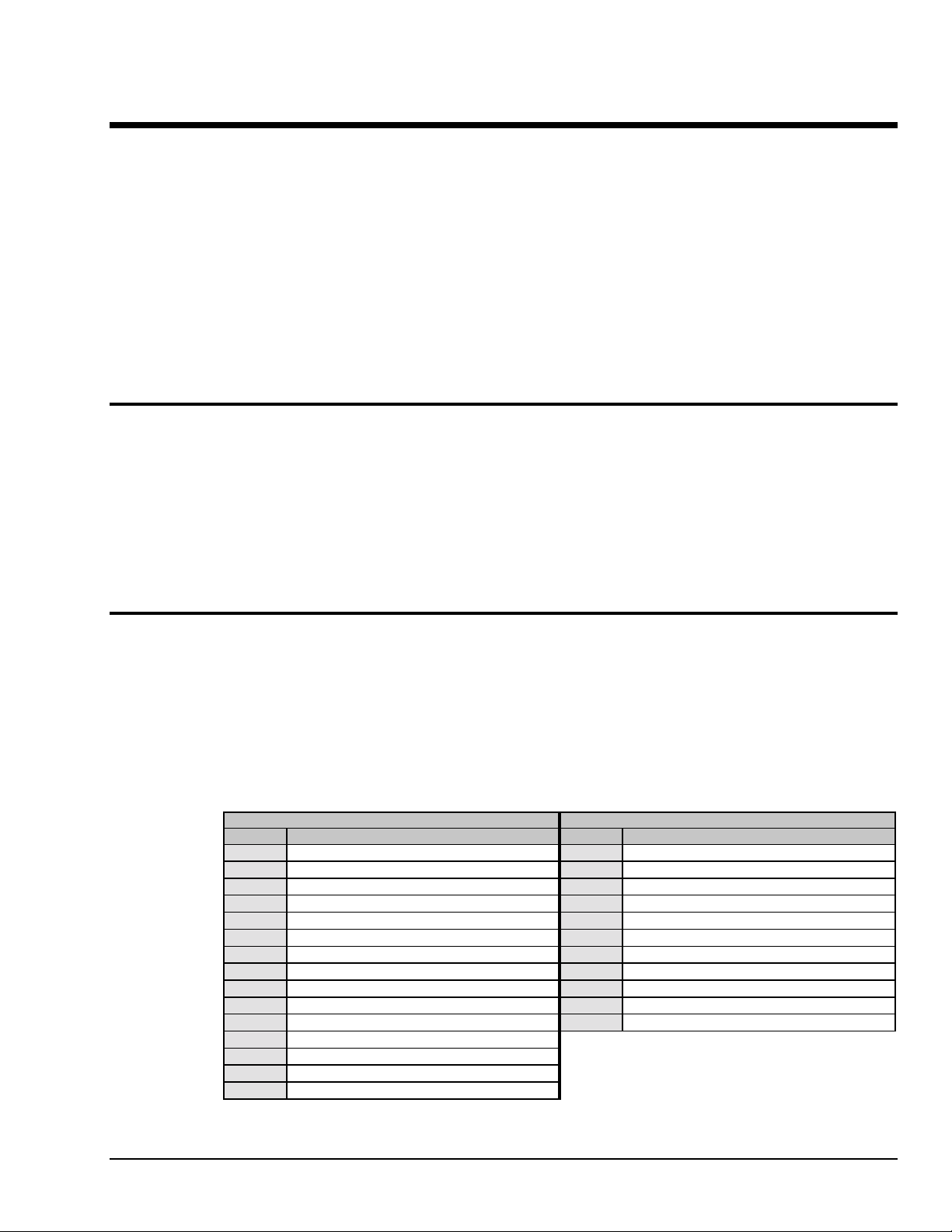
Triggering is t he process of changing a DAC
output at the occurrence of a trigger event.
The three trigger events which can trigger a
DAC port are: a Trigger On (
IEEE Group Execute Trigger (
external trigger pulse applied to the external
trigger/SRQ input. Any DAC port may be
configured to trigger on one or more of the s e
trigger sources. These trigger sources and
their relationship to a DAC port are shown in
the following diagram.
As shown in the diagram, the trigger sources
are routed to the ports by using the trigger
mask c ommands. The trigge r mask
commands are illustrated as switches. The
trigger mask commands are used to enable a
trigger source to trigger the selected DAC
port. All trigger signals are then combined to
allow a port to be triggered upon the
occurrence of any of the three trigger events.
@) command, an
GET) or an
Triggering is provided as a means of
synchronizing multiple DAC ports. Voltages
may be output at two or more ports
simultaneously by programming each port for
the desired voltages and trigger event(s).
When the trigger event occurs, the
programmed voltages will appear at the ports
simultaneously.
24 DAC488 Operation DAC488 User’s Manual
Page 31
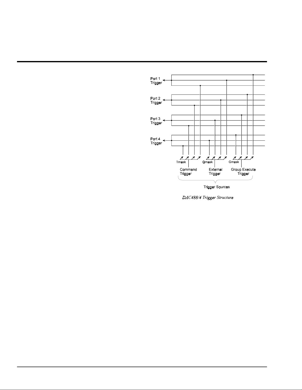
For example, a typical configuration may require Port 1 to have all trigger sources disabled, Port 2
configured to trigger on an IEEE Group Execute Trigger, Port 3 to trigger on an external trigger, and Port 4
to trigger on any of the three trigger sources.
The commands to configure the ports for this configuration are shown below:
PRINT#1,"OUTPUT09;G0 Q0 T0 X"
PRINT#1,"OUTPUT09;G2 X"
PRINT#1,"OUTPUT09;Q4 X"
PRINT#1,"OUTPUT09;G8 Q8 T8 X"
• Line 1:
G0 disables all ports from
triggering on an IEEE Group Execute
Trigger,
triggering on an external trigger,
Q0 disables all ports from
T0
disables all ports from triggering on a
command trigger (
@), and X executes the
commands.
• Line 2:
G2 enables port 2 for triggering
on an IEEE Group Execute Trigger and
X executes the command.
• Line 3:
on an external trigger and
Q4 enables port 3 for triggering
X executes the
command.
• Line 4:
on an IEEE Group Execute Trigger,
G8 enables port 4 for triggering
Q8
enables port 4 for triggering on an
external trigger,
triggering on an a command trigger (
X executes the commands.
and
T8 enables port 4 for
@),
After these commands are executed, the
trigger sources will be routed to the ports as
illustrated in the figure.
Trigger Processing & Trigger Overrun
Operation of the DAC488 is controlled by an internal 1 millisecond timer. Each DAC port is updated at a
maximum rate of once every millisecond. When a trigger event occurs, the DAC will output the
programmed voltage within 1 millisecond of receiving the trigger. If a second trigger event occurs before
the DAC has finished processing the first trigger, the second trigger will be held pending and a trigger
overrun error will occur. The error condition may be cleared by issuing the Error Query command (E?) and
then reading the response from the DAC488. After the first trigger is processed, the pending trigger will
then be processed. Any additional triggers which may occur while a trigger is held pending will be ignored.
DAC488 User’s Manual DAC488 Operation 25
Page 32

Internal Buffer
Buffer Data
The DAC488 contains an internal buffer consisting of 8,192 locations numbered 0 to 8,191. The buffer is
shared by all ports. Each port may be given a different section of the buffer or ports may use the same
buffer locations without conflict.
This buffer may be loaded with voltage values to be output when the Stepped or Waveform modes are used.
All data in the internal buffer is saved in Non-Volatile RAM. Therefore buffer data which was previously
loaded will be available at power on. Examples showing the use of the internal buffer are given in the
upcoming descriptions of Stepped and Waveform Control modes.
The following diagram shows the factory
default allocation of the internal buffer to
each of the DAC ports on the DAC488/4. On
the DAC488/2, only the Port 1 and Port 2
sections of the internal buffer are allocated.
Buffers are defined using the Buffer
Definition (
this command specify the starting location
start) and the number of locations (size)
(
in the defined buffer. Once the buffer is
defined it may be loaded with voltage values
using the Buffer Data (
Before using the Buffer Data command, the
Buffer Location (L) command should be used
to set the location pointer to the desired
value. The location pointer points to the area
where data will be stored when the Buffer
Data command is used. After each use of the
Buffer Data command, the location pointer is
incremented.
F
) command. The parameters of
B) co mmand.
26 DAC488 Operation DAC488 User’s Manual
Page 33

Buffer Save-and-Restore Program
This BASIC program DACBUFR.BAS may be used to save the contents of the DAC488 internal buffer to
disk. It can also be used to load the saved values from disk into the internal buffer.
10 'BASIC program to save and restore the DAC488 buffer contents
20 '
30 'Initialize the IOtech IEEE488 Driver
40 OPEN "\dev\ieeeout" FOR OUTPUT AS #1
50 IOCTL #1, "BREAK"
60 PRINT #1, "RESET"
70 OPEN "\dev\ieeein" FOR INPUT AS #2
75 ON TIMER(5) GOSUB 2000
80 CLS
90 PRINT "DAC488/4 Waveform Buffer Save and Restore Program"
100 PRINT : PRINT " 1 - Save the Waveform Buffer "
110 PRINT " 2 - Restore the Waveform Buffer "
120 PRINT " 3 - Exit the program"
130 PRINT : INPUT "Select the desired function "; FUN
140 IF FUN < 1 OR FUN > 3 THEN PRINT "Invalid selection!": GOTO 100
150 IF FUN = 3 THEN END
160 IF FUN = 1 THEN GOSUB 500 ELSE GOSUB 1000
170 GOTO 80
500 ' Save DAC488/4 waveform buffer
510 '
515 WCNT = 0: TIMER ON
520 OPEN "buffer.sav" FOR OUTPUT AS #3
530 PRINT #1, "output 09;p1c0l0x"
540 PRINT "Saving the DAC488/4 waveform buffer"
550 FOR LOP = 1 TO 2048
560 PRINT #1, "output 09;b?b?b?b?"
570 PRINT #1, "enter 09"
580 LINE INPUT #2, SS$
590 PRINT #3, SS$
600 NEXT LOP
610 CLOSE #3
620 TIMER OFF
630 RETURN
1000 ' Restore DAC488/4 waveform buffer
1010 '
1020 OPEN "buffer.sav" FOR INPUT AS #3
1030 PRINT #1, "output 09;p1c0l0x"
1040 PRINT "Restoring the DAC488/4 waveform buffer"
1045 WCNT = 0: TIMER ON
1050 FOR LOP = 1 TO 2048
1060 LINE INPUT #3, SS$
1070 RS$ = MID$(SS$, 1, 12) + "x" + MID$(SS$, 13, 12) + "x" + MID$(SS$, 25, 12) + "x" +
MID$(SS$, 37, 12) + "x"
1080 PRINT #1, "output 09;"; RS$
1090 NEXT LOP
1100 CLOSE #3
1110 TIMER OFF
1120 RETURN
2000 PRINT "Working - "; : WCNT = WCNT + 1
2010 IF WCNT > 6 THEN PRINT : WCNT = 0
2020 RETURN
DAC488 User’s Manual DAC488 Operation 27
Page 34

Control Modes
Four modes of DAC port operation are available: Direct, Indirect, Stepped, and Waveform. Each port is
independent and may be operated in a different mode. The modes of operation are described below.
Direct Control Mode
Each of the DAC ports may be directly controlled from the IEEE 488 bus. In the Direct Control mode, a
DAC voltage is output upon receipt of the Execute (
selecting the DAC port, the range or autorange, specifying the DAC output voltage, and issuing the Execute
command.
One use of the Direct mode is to output voltages at one or more DAC ports directly under program control
from an IEEE controller. To output 4 volts on port 1 the following command string could be used:
PRINT#1,"OUTPUT09;C0 P1 A0 R2 V4 X"
In this example, C0 selects Direct Control mode, P1 selects port 1, A0 disables Autor anging, R2 selects the
±5 Volt range and
output 4 volts at port 1.
Indirect Control Mode
Indirect control implies that the DAC output will change only when a trigger event occurs. Indirect control
is accomplished by selecting the DAC port, the range or autorange, specifying the DAC output voltage and
the desired trigger source. When the trigger event occurs, the programmed voltage will be output.
One use of the Indirect mode is to output voltages at one or more DAC ports upon the occurrence of a
trigger event. The command string shown below causes the DAC488 to output 7.5 volts at Port 2 upon
receipt of an external trigger signal.
PRINT#1,"OUTPUT09;C1 P1 Q1 A0 R2 V4 X"
X) command. Direct control is accomplished by
V4 is the voltage to be output (4 volts). This command string causes the DAC488 to
In this example, C1 selects the Indirect control mode, P1 selects port 1, Q1 enables port 1 to trigger on the
positive edge of an external trigger sense pulse,
V4 is the voltage to be output (4 volts).
Stepped Control Mode
The Stepped control mode may be used to control
the DAC in a stepped manner. In this mode, a
sequence of DAC voltages are loaded into the
DAC488 internal buffer. After the voltages are
loaded into the buffer, the DAC output can then
be stepped through each of the values b y using
any of the three trigger sources. When the last
voltage in the buffer is output, the DAC488 will
automatically return to the first location defined
by the Buffer Definition (
allowing the sequence to be repeated.
One application of Stepped mode may be to use
the DAC488 to output a series of test voltages
which may control another device. The example
shows how the DAC488 would be configured to
output the next vo ltage in a sequence of voltages
each time an external trigger is received.
In this example, the voltage at port 1 is stepped to the next value in the buffer each time an external trigger
is received. Each T on the graph represents a trigger event. The voltage sequence is 1 volt, 3 volts, 4 volts.
F) command thereby
A0
disables autoranging, R2 selects the ±5 Volt range and
28 DAC488 Operation DAC488 User’s Manual
Page 35
The commands required to load the internal buffer for this example are:
PRINT#1,"OUTPUT09;C2 P1 F0,3 L0 Q1 X"
PRINT#1,"OUTPUT09;B1,1X B2,3X B2,4X"
PRINT#1,"OUTPUT09;L0 X"
• Line 1:
C2 selects Stepped Control mode, P1 selects port 1, F0,3 defines a buffer with the fir s t
location as location 0 and the number of values in the sequence to 3,
to 0 (first location) and
• Line 2:
B1,1X selects the ±1 volt range, 1 volt for firs t point, B2,3X selects the ±5 volt range, 3 volts
for second point and
• Line 3:
L0
the location pointer will start at location 3, not location 0.
The output of the sequence is controlled by the rate at which external triggers occur. In the graph
previously shown, each T represents an external trigger event.
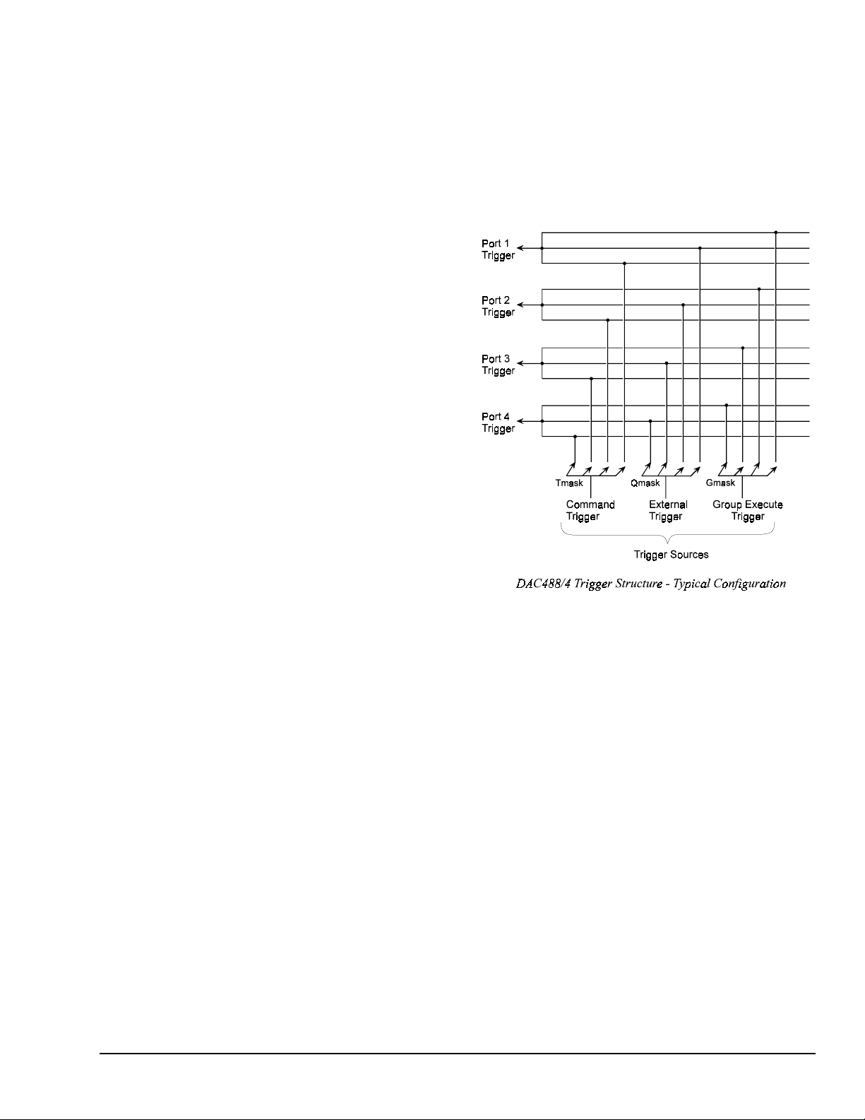
Waveform Control Mode
The Waveform control mode may be used to control the
DAC in an automatic manner. A buffer is defined using
the Buffer Definition (
are loaded into the buffer using the Buffer Location (
command and the Buffer Data (
DAC488 is triggered, these preloaded voltage values
are then output at a regular interval. The time interval
between the output of each value is set by using the
Interval (
waveform is set by using the Number of Cycles (
command.
I) command. The number of cycles of the
L0 sets the location pointer back
Q1 enables port 1 to trigger on an external trigger.
B2,4X selects the ±5 volt range, 4 volts for third point.
sets the location pointer back to location 0 before the port is triggered. If this is not done,
F) command and volt age values
L)
B) command. Once the
N)
One application of waveform mode may be to use the
DAC488 as a precise function generator. The
waveform example shows how the DAC488 would be
configured to output a 6 volt peak to peak 500 Hz
square wave centered at zero.
More complex waveforms may be generated by loading the b uffer with values computed using a high-level
language program. Sample programs are i ncluded with the DAC488 which will load the buffer with voltage
values to genera t e a Sine, Triangle, Ramp and other waveforms.
The commands required to load the internal buffer for this example are:
PRINT#1,"OUTPUT09;C3 P1 F0,2 G1 L0 I1 X"
PRINT#1,"OUTPUT09;B2,3X B2,-3X N0 X"
PRINT#1,"OUTPUT09;L0 X"
PRINT#1,"OUTPUT09;TRIGGER"
• Line 1:
location as location 0 and the number of points in the sequence to 2,
the location pointer to 0 (the first location) and
C3
selects Waveform control mode,
P1
selects port 1,
I1 sets the time interval between points to 1
F0,2
defines a buffer with the first
G1 selects trigger on GET, L0 sets
millisecond.
• Line 2:
volts for second point,
• Line 3:
B2,3X
selects the ±5 volt range, 3 volts for fir s t point and
N0 sets the number of cycles to continuous.
L0 sets the buffer location pointer back to location 0 before the port is triggered. If this is not
B2,-3X
selects the ±5 volt range, -3
done, the location pointer will start at location 2, not location 0.
• Line 4: When the IEEE Group Execute Trigger is executed, the DAC488 will output the waveform at
port 1 co ntinuously.
DAC488 User’s Manual DAC488 Operation 29
Page 36

Multiple Port Synchroni z a ti on
Multiple DAC port output changes may be synchronized in any of the triggered modes of operation
(Indirect, Stepped and Waveform). This is done by using the trigger mask commands to enable the ports to
trigger on the same trigger event(s).
Synchronization in Waveform mode is automatically accomplished by programming multiple ports with the
same time interval using the Interval (
command. The BASIC program
synchronized wavefor ms may be gene rated. Thi s program is included below.
Synchronized Waveforms Program
The following BASIC program DAC4WAVE.BAS is used with the DAC488 to generate a waveform at a user
selectable frequency and 20 volts peak-to-peak centered at 0 volts:
10 REM Basic program to load the DAC488/4 buffer w multiple waveforms
20 REM Initialize the IOtech IEEE488 Driver
30 CLS : KEY OFF
40 OPEN "\dev\ieeeout" FOR OUTPUT AS #1
50 IOCTL #1, "BREAK"
60 PRINT #1, "RESET"
70 OPEN "\dev\ieeein" FOR INPUT AS #2
80 PRINT "DAC488 Waveform Demonstration Program"
90 PRINT
100 PRINT"Set address of DAC488 to 09 and connect to controller"
110 PRINT
120 PRINT"Hit any key to start"
130 IF INKEY$="" THEN GOTO 130
140 PRINT:PRINT #1, "CLEAR 09"
150 PRINT #1, "output 09;P3XE?" 'Determine if DAC488/4 or DAC488/2
160 PRINT #1, "ENTER 09"
170 INPUT#2,A$
180 IF A$ = "E0" THEN DAC2$ = "N" ELSE DAC2$ = "Y"
190 IF DAC2$ = "Y" THEN MODEL$ = "2" ELSE MODEL$ = "4"
200 PRINT "Initializing the DAC488/";MODEL$;" this will take a while"
210 REM First a 256 point sinewave
220 PRINT #1, "output 09;c3l0x"
230 POINTS = 256: REM number of points in the sine wave
240 PI = 3.1415926535#
250 INC = (2! * PI) / POINTS
260 FOR LOOP = 1 TO POINTS
270 PVAL = 4095*SIN(LOOP * INC)
280 PRINT #1, "output 09;b3,#";CINT(PVAL);"x":NEXT
290 REM Now a triangle wave
300 INC = 4096 / 64
310 FOR LOOP = 0 TO 4095 STEP INC
320 PRINT #1,"output 09;b3,#";LOOP;"x":NEXT
330 FOR LOOP = 4095 TO -4095 STEP -INC
340 PRINT #1,"output 09;b3,#";LOOP;"x":NEXT
350 FOR LOOP = -4095 TO 0 STEP INC
360 PRINT #1,"output 09;b3,#";LOOP;"x":NEXT
370 REM Now a square wave
380 PRINT #1,"output 09;b3,#4095xb3,#-4095x"
390 REM Main Loop
400 CLS
I
) command and the same buffer size using the Buffer Definition (F)
DAC4WAVE.BAS included on the program disk shows how multiple,
30 DAC488 Operation DAC488 User’s Manual
Page 37

410 IF MODEL$ = "2" THEN GOTO 420 ELSE GOTO 440
420 INPUT" Select a port 1,2 ";PORT
430 GOTO 450
440 INPUT" Select a port 1-4 ";PORT
450 IF PORT < 1 OR PORT > 4 GOTO 410
460 IF PORT > 2 AND DAC2$ ="Y" THEN GOTO 410
470 PRINT
480 INPUT"Select an interval in milliseconds (1-255) ";INTRVL
490 IF (INTRVL <= 0) OR (INTRVL > 255) GOTO 480
500 PRINT" Select a waveform (1-6) ";WAVE
510 PRINT" 1 - Sinewave "
520 PRINT" 2 - Rectified Sine Wave"
530 PRINT" 3 - Triangle "
540 PRINT" 4 - Ramp "
550 PRINT" 5 - Inverted Ramp "
560 PRINT" 6 - Square Wave "
570 INPUT WAVE
580 IF WAVE < 1 OR WAVE > 6 GOTO 500
590 IF WAVE = 1 GOTO 660
600 IF WAVE = 2 GOTO 700
610 IF WAVE = 3 GOTO 740
620 IF WAVE = 4 GOTO 780
630 IF WAVE = 5 GOTO 820
640 IF WAVE = 6 GOTO 860
650 PRINT: PRINT: GOTO 410
660 REM sinewave output routine
670 PRINT #1,"output 09;p";PORT"c3f0,256l0i";INTRVL;"n0t0x"
680 PRINT #1,"output 09;t"; (2^(PORT-1));"x@"
690 GOTO 650
700 REM rectified sinewave output routine
710 PRINT #1,"output 09;p";PORT"c3f0,128l0i";INTRVL;"n0t0x"
720 PRINT #1,"output 09;t"; (2^(PORT-1));"x@"
730 GOTO 650
740 REM triangle wave output routine
750 PRINT #1,"output 09;p";PORT"c3f256,256l256i";INTRVL;"n0t0x"
760 PRINT #1,"output 09;t"; (2^(PORT-1));"x@"
770 GOTO 650
780 REM ramp wave output routine
790 PRINT #1,"output 09;p";PORT"c3f256,64l256i";INTRVL;"n0t0x"
800 PRINT #1,"output 09;t"; (2^(PORT-1));"x@"
810 GOTO 650
820 REM inverted ramp wave output routine
830 PRINT #1,"output 09;p";PORT"c3f384,64l384i";INTRVL;"n0t0x"
840 PRINT #1,"output 09;t"; (2^(PORT-1));"x@"
850 GOTO 650
860 REM square wave output routine
870 PRINT #1,"output 09;p";PORT"c3f512,2l512i";INTRVL;"n0t0x"
880 PRINT #1,"output 09;t"; (2^(PORT-1));"x@"
890 GOTO 650
DAC488 User’s Manual DAC488 Operation 31
Page 38

Digital I/O Port
The digital I/O port on the DAC488 may be used to read eight TTL level inputs and control eight TTL level
outputs. The digital outp ut port may also be configured for high voltage/high current operation. Once the
output port is configured for high level operation, the output can control relays and other high leve l devices.
One use of the high level outputs may be to energize a relay under program control. The following
Standard and CE diagrams each show how a digital output line can control a relay which in turn, connects
the DAC Port 4 output voltage to an external volt controlled device. The Digital Output (
would then be used to control the relay. Sending the command
deenergize the relay.
D0X
will energize the relay and a
D
) co mmand
D8X
will
32 DAC488 Operation DAC488 User’s Manual
Page 39
User-Defined System Defaults
The System Defaults (S) command is used to save the Calibration Constants in the Non-Volatile RAM. It
may also be used to save a particular configuration of the DAC488 as a power on default configuration. All
system and port commands may be used to configure the DAC488 and then this particular configuration
saved as the power on default configuration.
An application may require the DAC488 to power on in the following configuration:
• Autorange disabled
• Waveform Control Mode
• Interval = 1 millisecond
The commands to configure the DAC488 in the above configuration and then to save this configuration as
the power on default would be as follows:
PRINT#1,"OUTPUT09;A0 C3 I1 P2 R3 G2 X"
PRINT#1,"OUTPUT09;S1 X"
• Line 1:
A0 disables autoranging, C3 selects Waveform control mode, I1 sets the interval to 1
millisecond,
• Line 2:
S1 saves this configuration as the power on default configuration.
IEEE 488 Bus Support
The DAC488 implements many of the capabilities defined by the IEEE 488 1978 specification. These
capabilities are discussed in the following sections. However, the bus lines (uniline) and bus commands
(multiline) that the DAC488 does not support, or respond to, include the following:
REN
GTL
LLO
PPC
Remote Enable (uniline)
Go to Local
Local Lock Out
Parallel Poll Configure
• Port 2 selected
• Range = ±10 volts
• Trigger on Group Execute Trigger
P2
selects port 2, R3 sets the range to ±10 volts, G2 enables port 2 to trigger on
PPD
PPU
TCT
Parallel Poll Disable
Parallel Poll Unconfigure
Take Control
GET
.
Bus Lines
The following IEEE 488 bus management lines are supported by DAC488:
• Interface Clear (
• Service Request (
return a Serial Poll Status byte of at least 64 (decimal) showing that the
):
IFC
IFC places the DAC488 in the Talker/Listener Idle State.
): Whenever the DAC488 generates a Service Request (
SRQ
SRQ
), a Serial Poll will
SRQ was generated by the
DAC488. The following BASIC program illustrates one approach for handling service requests:
PRINT#1,"SPOLL09"
INPUT#2,SRQ09
IF SRQ09 < 64 THEN GOTO 500
IF SRQ09 = 65 THEN GOTO 600
IF SRQ09 = 66 THEN GOTO 700
IF SRQ09 = 68 THEN GOTO 800
Note:
To allow the DAC488 to detect each of the above conditions, the Service Request Mask (
Serial poll the DAC488
SRQs disabled
DAC port 1 ready routine
DAC port 2 ready routine
DAC port 3 ready routine
command must be enabled for each condition. More extensive tests of the Serial Poll Status
Byte are needed if multiple
Request Mask (
M) command in Chapter 7.
SRQ conditions are selected. For more details, refer to the Service
M)
DAC488 User’s Manual DAC488 Operation 33
Page 40

Bus Commands
The following IEEE 488 bus commands are supported by DAC488:
• Device Clear (
): Device Clear resets all devices, including the DAC488, to its power on state. The
DCL
DAC488 will be in the Listener Idle and Talker Idle state. The power on default settings for each
command will be programmed.
• Group Execute Trigger (
): When the DAC488 recognizes a
GET
GET, and the GET Trigger Mask (G)
command has been used to arm the DAC488, it outputs the programmed voltage or voltage sequence
(depending on which mode the DAC488 is in) at the selected port(s).
): When the DAC488 is addressed to Listen, it accepts characters from the
• My Listen Address (
MLA
Active Talker and interprets these characters as commands and command parameters.
): When the DAC488 is addressed to Talk, it returns a string specifying the
• My Talk Address (
MTA
selected port along with the selected range and output voltage which was programmed for that port.
The DAC488 can also return a status string for each port or the entire interface by using the User Status
(
U) command. Information about commands previously executed or data stored in the internal buffer
?
may be returned by using the Query (
• Selected Device Clear (
SDC
): Selected Device Clear resets a single device, in this case the DAC488, to
) co mmand.
its power on state. The DAC488 will be in the Listener Idle and Talker Idle state. The power on
default settings for each command will be programmed.
• Serial Poll Disable (
• Serial Poll Enable (
): Disables the DAC488 from responding to Serial Polls by the controller.
SPD
): When Serial Poll Enabled, the DAC488 sets itself to respond to a Serial
SPE
Poll with its Serial Poll Status byte if addressed to Talk. When the Serial Poll byte is accepted by the
controller, any pending
SRQs are cleared. The DAC488 will continue to try to output its Serial Poll
response until it is Serial Poll Disabled by the controller.
):
UNL
• Unlisten (
• Untalk (
UNT
UNL places the DAC488 in the Listener Idle State.
):
UNT places the DAC488 in the Talker Idle State.
Bus Addresses
The IEEE 488 interface standard permits up to 15 devices to be configured within one system. Each of
these devices must have a unique address to avoid confusion. In a similar fashion, every building in town
has a unique address to prevent one home from receiving another home's mail. Exactly how each device's
address is set is specific to the product's manufacturer. Some are set by DIP switches in hardware, others by
software. Consult the manufacturer's instructions to determine how to set the address.
Bus addresses are sent with bus (multiline) commands from the Active Controller. These commands
include My Listen Address (
Group (
Bus Terminators
The terminating characters sent on output by the DAC488 are set by using the Bus Terminator (Y)
command. Upon power on, the unit's IEEE 488 bus terminators are determined by the power-on
configuration saved using the System Defaults (
(carriage-return line-feed). The power on default terminators can be changed to any of the four available
LF
options listed under the Bus Terminator (
commands and the associated terminator options with them, are: (1)
= CR
terminator(s) may be selected using the Bus Terminator command and then this selection may be saved
using the System Defaults (
The DAC488 ignores all terminators received from the bus controller. Only the Execute (
used to signal the DAC488 that a command string has been completed. The only exception to this rule is
the Trigger On (
MLA), My Talk Address (MTA), Talk Address Group (TAG), and Listen Address
LAG).
S) command. The factory default terminator selection is CR
Y) command, described in Chapter 7. The four available
Y0 = CR LF, (2) Y1 = LF CR, (3) Y2
only, and (4) Y3 = LF only. If it is desired to have particular power on default terminator(s), the
S) co mmand.
X) co mmand i s
@) command which is processed immediately upon receipt.
34 DAC488 Operation DAC488 User’s Manual
Page 41

IEEE 488 Background 5
History…… 35
General Bus Structure…… 35
Bus Lines & Bus Commands…… 36
Bus Management Lines…… 36
Handshake Lines…… 37
Data Transfer Lines…… 37
Bus Command Groups…… 38
More On Service Requests…… 39
History
The IEEE 488 bus is an instrumentation communication bus adopted by the Institute of Electrical and
Electronic Engineers in 1975 and revised in 1978. Prior to the adoption of this standard, most
instrumentation manufacturers offered their own versions of computer interfaces. This placed the burden of
system hardware design on the end user. If his application required the products of several different
manufacturers, then he might need to design several different hardware and software interfaces. The
popularity of the IEEE 488 interface (sometimes called the General Purpose Interface Bus or GPIB) is due
to the total specification of the electrical and mechanical interface as well as the data transfer and control
protocols. The use of the IEEE 488 standard has moved the responsibility of the user from the design of the
interface, to the design of the high level software that is specific to the measurement application.
General Bus Structure
The main purpose of the IEEE 488 interface is to transfer information between two or more devices. A
device can either be an instrument or a computer. Before any information transfer can take place, it is first
necessary to specify which will do the talking (send data) and which devices will be allowed to listen
(receive data). The decision of who will Talk and who will Listen usually falls on the System Controller
which is, at power on, the Active Controller.
The System Controller is similar to a committee chairman. On a well run committee, only one person may
speak at a time and the chairman is responsible for recognizing members and allowing them to have their
say. On the bus, the device which is recognized to speak is the Active Talker. There can only be one
Talker at a time if the information transferred is to be clearly understood by all. The act of "giving the
floor" to that device is called Addressing to Talk. If the committee chairman cannot attend the meeting, or
if other matters require his attention, he can appoint an acting chairman to take control of the proceedings.
For the IEEE 488 interface, this device becomes the Active Controller.
At a committee meeting, everyone present usually listens. This is not the case with the IEEE 488 interface.
The Active Controller selects which devices will Listen and commands all other devices to ignore what is
being transmitted. A device is instructed to Listen by being Addressed to Listen. This device is then
referred to as an Active Listener. Devices which are to ignore the data message are instructed to Unlisten.
The reason some devices are instructed to Unlisten is quite simple. Suppose a college instructor is
presenting the day's lesson. Each student is told to raise their hand if the instructor has exceeded their
ability to keep up while taking notes. If a hand is raised, the instructor stops his discussion to allow the
slower students the time to catch up. In this way, the instructor is certain that each and every student
receives all the information he is trying to present. Since there are a lot of students in the classroom, this
exchange of information can be very slow. In fact, the rate of information transfer is no faster than the rate
at which the slowest note-taker can keep up . The instructor, though, may have a message for one parti cular
student. The instructor tells the rest of the class to ignore this message (Unlisten) and tells it to that one
student at a rate which he can understand. This information transfer can then happen much quicker, because
it need not wait for the slowest student.
DAC488 User’s Manual IEEE 488 Background 35
Page 42

The IEEE 488 interface transfers information in a similar way, with a method of data transfer called
handshaking. For data transfer on the IEEE 488 interface, the Active Controller must:
• Unlisten all devices to protect against eavesdroppers.
•
Designate a device who will talk by addressing it to Talk.
•
Designate all the devices who will listen by addressing them to Listen.
• Indicate to all devices that the data transfer can take place.
Bus Lines & Bus Commands
Bus Management Lines
For the general control and coordination of bus activities, five hardware lines on the IEEE 488 interface are
used for bus management. Signals on these lines are often referred to as uniline (single line) commands.
The signals are active low (i.e., a low voltage represents an asserted logic of “1”, a nd a high voltage
represents an unasserted logic of “0”).
• Interface Clear (
devices in a known state. Although device configurations vary, the
IFC
): The
IFC line is used only by the System Controller. It is used to place all bus
IFC command usually places the
devices in the Talk and Listen Idle states (neither Active Talker nor Active Listener).
): When the System Controller sends the
• Remote Enable (
REN
to remote operation. Generally, the
REN command should be issued before any bus programming is
REN command, bus devices will respond
attempted. Only the System Controller has control of the Remote Enable line.
• Attention (
ATN
): The
ATN line is one of the most important lines for bus management. If Attention is
asserted, then the information contained on the data lines is to be interpreted as a multiline command.
If it is not, then that information is to be interpreted as data for the Active Listeners. The Active
Controller is the only bus device that has control of this line.
): The
• End Or Identify (
EOI
device that is sending the data asserts
EOI line is used to signal the last byte of a multibyte data transfer. The
EOI during the transfer of the last data byte. The EOI signal is
not always necessary, for the end of the data may be indicated by some special character such as
carriage return (
Poll by simultaneously asserting
• Service Request (
asserts
SRQ. It is then the responsibility of the controller to determine which device requested service.
CR) and/or line feed (LF). The Active Controller also uses EOI to perform a Parallel
EOI and ATN.
): When a device desires the immediate attention of the Active Controller, it
SRQ
This is accomplished with a Serial Poll or a Parallel Poll.
36 IEEE 488 Background DAC488 User’s Manual
Page 43

Handshake Lines
The IEEE 488 interface uses three handshake lines in an "I'm ready - Here's the data - I've got it" sequence.
This handshake protocol assures reliable data transfer, at the rate determined by the slowest Listener. One
line is controlled by the Talker, while the other two are shared by all Active Listeners. The handshake lines,
like the other IEEE 488 lines, are active low.
• Data Valid (
(active low) which indicates that all Listeners have accepted the previous data byte transferred. The
Talker then outputs data on the bus and waits until
addressed Listeners are ready to accept the information. When
the Talker asserts
• Not Ready for Data (
ready to accept new data. The Talker must wait for each Listener to unassert this line (high) which they
will do at their own rate when they are ready for more data. This assures that all devices that are to
accept the information are ready to receive it.
• Not Data Accepted (
the Talker that each device addressed to Listen has accepted the information. Each device releases
NDAC
data byte.
Data Transfer Lines
To transfer bit-parallel/byte-serial information between devices on the bus, the IEEE 488 interface provides
eight data lines (
): The
DAV
(high) at its own rate, but the
DIO1 through DIO8). These data lines are bidirectional and are active low.
DAV line is controlled by the Talker. The Talker verifies that NDAC is asserted
NRFD is unasserted (high) which indicates that all
NRFD and NDAC are in the proper state,
DAV (active low) to indicate that the data on the bus is valid.
): The
NRFD
NDAC
): The
NRFD line is used by the Listeners to inform the Talker when they are
NDAC
line is also controlled by the Listeners. This line indicates to
NDAC
will not go high until the slowest Listener has accepted the
DAC488 User’s Manual IEEE 488 Background 37
Page 44

Bus Command Groups
Bus (multiline) commands are bytes sent by the Active Controller over the data bus with Attention (ATN)
asserted. These commands are sent to all devices and are divided into the following 5 groups:
• Addressed Command Group (
been addressed to be a Listener. There are 5 bus line addressed commands:
TCT.
): These commands affect only those devices which have previously
ACG
GET, GTL, PPD, SDC, and
• Universal Command Group (
): These commands cause every instrument on the bus to carry out
UCG
the bus function specified (if the instrument is capable of it). There are 5 bus line universal commands:
DCL, LLO, PPU, SPD
• Listen Address Group (
, and
SPE
.
): These commands address to Listen specified bus devices. There are 31
LAG
(0 to 30) Listen addresses associated with this group. The 3 most significant bits of the data bus are set
to
001 while the 5 least significant bits are the address of the device being told to Listen.
• Talk Address Group (
): These commands address to Talk specified bus devices. There are 31 (0
TAG
to 30) Talk addresses associated with this group. The 3 most significant bits of the data bus are set to
010 while the 5 least significant bits are the address of the device being told to Talk.
• Secondary Command Group (
): These commands are used to specify a subaddress or subfunction
SCG
within a given bus device. These are any one of the 32 possible commands (0 to 31) in this group.
They must immediately follow a Talk or Listen address.
• Three bus commands not found in the above 5 groups are:
MLA, MTA, and PPC.
All of the IEEE 488 bus commands are further described individually, as follows:
): This command causes all bus devices to be initialized to a pre-defined or power
• Device Clear (
DCL
up state.
): This command usually signals a group of devi ces to begin executing a
• Group Execute Trigger (
GET
triggered action. This allows actions of different devices to begin simultaneously.
• Go To Local (
• Local Lock Out (
): This command allows the selected devices to be manually controlled.
GTL
): This command prevents manual control of the instrument's functions.
LLO
• My Listen Address (
): This command addresses a device to Listen. The device accepts data from
MLA
the Active Talker and outputs this data through the serial inter face. It substitutes the selected serial
terminators for the received IEEE 488 bus terminators.
• My Talk Address (
): This command addresses a device to Talk. The device retrieves data from
MTA
the serial input buffer and outputs it to the IEEE 488 bus. It substitutes the selected IEEE 488 bus
terminators for the received serial terminators. The device will continue to output serial input buffer
data as long as the IEEE 488 controller allows.
• Parallel Poll Configure (
): This command configures devices capable of performing a Parallel
PPC
Poll via the data bit they are to assert in response to a Parallel Poll.
• Parallel Poll Disable (
• Parallel Poll Unconfigure (
• Selected Device Clear (
): This command disables the Parallel Poll response of selected devices.
PPD
): This disables all devices from responding to a Parallel Poll.
PPU
): This command causes a single device to be initialized to a pre-defined or
SDC
power up state.
38 IEEE 488 Background DAC488 User’s Manual
Page 45

• Serial Poll Disable (
byte.
): The command disables all devices from sending their Serial Poll status
SPD
• Serial Poll Enable (
addressed to Talk, to output its Serial Poll status byte.
• Take Control (
another device which has the ability to control.
• Unlisten (
• Untalk (
UNL
): This command places the device in the Talk Idle state.
UNT
More On Service Requests
Most of the commands covered, both uniline and multiline, are the responsibility of the Active Controller to
send and the bus devices to recognize. Most of these happen routinely by the interface and are totally
transparent to the system programmer. Other commands are used directly by the user to provide optimum
system control. Of the uniline commands,
designer has easy access to this line by most devices. Service Request is the method by which a bus device
can signal to the Controller that an event has occurred. It is similar to an interrupt in a microprocessor
based system.
Most intelligent bus peripherals have the ability to assert
when its measurement is complete, if its input is overloaded or for any of an assortment of reasons. A
power supply might
burden from the System Controller to periodically inquire, "Are you done yet?". Instead, the Controller
says, "Do what I told you to do and let me know when you're done" or "Tell me when something is wrong."
Since
SRQ is a single line command, there is no way for the Controller to determine which device requested
the service without additional information. This information is provided by the multiline commands for
Serial Poll and Parallel Poll.
): This command, when
SPE
): This command passes bus control responsibilities from the current Controller to
TCT
ATN is unasserted, will cause a device that is
): This command places the device in the Listen Idle state.
SRQ is very important to the test system and the software
SRQ. A digital multimeter (DMM) might assert it
SRQ
if its output has current limited. This is a powerful bus feature that removes the
• Serial Poll: Suppose the Controller receives a service request. For this example, let us assume there
are several devices which could assert
to each device sequentially. If any device responds with
that it was the device that asserted
SRQ. The Controller issues a Serial Poll Enable (SPE) comman d
DIO7 asserted, it indicates to the Controller
SRQ
. Often times the other bits will indicate why the device wanted
service. This Serial Polling sequence, and any resulting action, is under control of the software
designer.
• Parallel Poll: The Parallel Poll is another way the Controller can determine which device requested
service. It provides the who, but not necessarily the why. When bus devices are configured for Parallel
Poll, they are assigned one bit on the data bus for their response. By using the Status bit, the logic level
of the response can be programmed to allow logical
one device. When
SRQ is asserted, the Controller (under the user's software) conducts a Parallel Poll.
OR/AND conditions on one data line by more than
The Controller must then analyze the eight bits of data received to determine the source of the request.
Once the source is determined, a Serial Poll might be used to determine the why.
Of the two polling types, the Serial Poll is the most popular due to its ability to determine the who and why.
In addition, most devices support Serial Poll only.
DAC488 User’s Manual IEEE 488 Background 39
Page 46

−
Notes
40 IEEE 488 Background DAC488 User’s Manual
Page 47

DAC488 Calibration 6
Introduction…… 41
Calibration Procedures…… 41
Manual Calibration Procedure…… 42
Part I: Connections & Preparations…… 42
Part II: Acquiring t he Gai n Cal i brat i on Constants…… 42
Part III: Acquiri ng the Offset Calibration Const ant…… 43
BASIC Calibration Program…… 43
Automatic Calibration Procedure…… 47
Part I: Connections & Preparations…… 47
Part II: Automatic Calibration Process…… 48
Part III: Automatic Calibration Report…… 49
Introduction
Each port of the DAC488 should be calibrated every 12 months or if the performance verification report
(described later in this chapter) shows that the DAC488 is not operating within the specifications.
Calibration of the DAC488 involves computing the correct Calibration Constants for the offset and gain for
each range and polarity. These constants are then stored in the DAC488 Non-Volatile RAM for subsequent
use. When a DAC port is commanded to output a voltage, the Calibration Constants are sent to internal
D/A converters which set the offset and gain for the given range and polarity. The DAC488 may be
calibrated by the following two methods:
1. Calibration may be performed by a host controller using the BASIC calibration program included with
the DAC488. The program will then print a calibration report when finished.
2. Calibration may be performed automatically by the DAC488 acting as a bus controller connected to a
Keithley 199 DMM. A calibration report will then be printed if the DAC488 is connected to an IEEE
printer.
The calibration enable switch on the rear panel must be in the closed (depressed) position to allow the new
Calibration Constants to be saved in the Non-Volatile RAM. If the switch is not in this position, these
constants may be changed but they will not be saved. If the DAC488 is then turned off, the Calibration
Constants will revert to their last saved values. After calibration is completed, the calibration switch should
be set to the open position, (switch cap flush with the read panel) to prevent accidental changing of these
constants.
Calibration Procedures
The calibration procedures used to compute the Gain and Offset Calibration Constants, as explained below,
are the same as those used in the BASIC and in the automatic calibration programs. The example shows
how to compute the positive gain, negative gain, and offset calibration constants for the ±10 volt range of
Port 1. The equipment needed to calibrate the DAC488 manually are as follows:
• A Voltmeter with a full scale error of 0.01% or better.
• An IEEE controller or a PC with an IEEE interface.
• An IEEE 488 cable.
• Test Leads.
• The analog output connector included with the DAC488.
Commands that must be sent are listed after each step. If you are using the Personal488 interface, you can
send commands to the DAC488 directly by using the Keyboard Controller program listed in the “Power-Up
& Performance Tests” section in Chapter 3. For example, to send the command
TEST LED on the DAC488 front panel), you would type
press the
<Enter> key.
W1X (This will turn on the
OUTPUT 09;W1X after the CMD> prompt, then
DAC488 User’s Manual DAC488 Calibration 41
Page 48

Manual Calibration Procedure
Part I: Connections & Preparations
1. Connect the DAC488 to the IEEE controller using an IEEE 488 cable.
2. Connect the negative input of the voltmeter to the Port 1 L (Low) output.
3. Connect the positive input of the voltmeter to the Port 1 H (High) output.
4. Set the IEEE bus address of the DAC488 to 9.
5. Turn the DAC488 on, and allow it to warm up for at least one hour before beginning the calibration
procedure.
Part II: Acquiring the Gain Calibration Constants
1. After the DAC488 has warmed up for at least one hour, initialize the DAC488 by sending an IEEE 488
Interface Clear (
CLEAR 09
2. Select Port 1, Direct Control Mode, Autoranging disabled, select the +10 volt range, set the Offset to 0,
set the Positive and Negative Gain constants to 128, program the port to output 0 volts. Command sent
to the DAC488:
OUTPUT 09; P1 C0 A0 R3 H0 J128,128 V0 X
3. Measure and record the port 1 output voltage. Call this voltage ZVAL.
4. Program the DAC488 port 1 to output 10 volts. Command sent to the DAC488:
OUTPUT 09; V10 X
IFC). Command sent to the DAC488:
5. Measure and record the port 1 output voltage. Call this voltage PVAL.
6. Program the DAC488 port 1 to output -10 volts. Command sent to the DAC488:
OUTPUT 09; V-10 X
7. Measure and record the port 1 output voltage. Call this voltage NVAL.
8. Set the Positive and Negative Gain constants to maximum (255) and program the port to output 10
volts. Command sent to the DAC488:
OUTPUT 09; J255,255 V10 X
9. Measure and record the port 1 output voltage. Call this voltage MVAL.
10. Set the Positive and Negative Gain constants to minimum (0) and program the port to output 10 volts.
Command sent to the DAC488:
OUTPUT 09; J0,0 V10 X
11. Measure and record the port 1 output voltage. Call this voltage NOVAL.
12. The Gain Calibration Constants are computed using the following formulas:
• Gain adjustment per bit = (
• Pos. Error (in volts) =
MVAL - NOVAL) / 256
PVAL - ZVAL - 10
• Pos. Gain Calibration Constant = (128 - Pos. Error) / Gain adjust per bit
• Neg. Error (in volts) =
NVAL - ZVAL - 10
• Neg. Gain Calibration Constant = (128 + Neg. Error) / Gain adjust per bit
13. Once the Gain Calibration Constants have been computed, the positive and negative gains should be set
to these new values. This can be done using the Gain Calibration (
J) command. For example, if the
positive and negative Gain Calibration Constants are 131 and 148 respectively, the command
J131,148 X should be sent to the DAC488.
42 DAC488 Calibration DAC488 User’s Manual
Page 49

After setting the new gain values, the Offset Calibration Constant should be computed. (The Offset
Calibration Constant is affected by the Gain Calibration Constant.)
Part III: Acquiring the Offset Calibration Constant
1. After setting the new gain values, set the Offset of Port 1 to minimum (-255) and program Port 1 to
output 0 volts. Command sent to the DAC488:
OUTPUT 09; H-255 V0 X
2. Measure and record the port 1 output voltage. Call this voltage NOFFVAL.
3. Set the Offset of Port 1 to maximum (+255) and program Port 1 to output 0 volts. Command sent to
the DAC488:
OUTPUT 09; H255 V0 X
4. Measure and record the port 1 output voltage. Call this voltage POFFVAL.
5. Set the Offset of Port 1 to 0 and program Port 1 to output 0 volts. Command sent to the DAC488:
OUTPUT 09; H0 V0 X
6. Measure and record the port 1 output voltage. Call this voltage ZERR.
7. The Offset Calibration Constant is computed using the following formulas:
• Offset adjustment per bit = (
• Offset Calibration constant = Negative
8. The Offset Calibration Constant should now be set to the newly computed value by using the Offset
Calibration (H) command. For example, if the Offset Calibration Constant is 18, the command H18 X
should be sent to the DAC488.
BASIC Calibration Program
The following BASIC program (filename DACCAL.BAS or CALIBR8.BAS), which is included on disk, will
calibrate the DAC488 using a Personal488 IEEE 488 interface card, Driver488 software, and a Keithley
Instruments Model 196 DMM. Other DMMs (digital multimeters) may be used although the program will
need to be modified. All device dependent commands are contained in subroutines thus allowing these
commands to be easily changed to suit the DMM being used.
10 'DAC488 Calibration Program
20 KEY OFF
30 ' Requires a Keithley 196 DMM or equivalent
40 '
50 KAD$="26":DAD$="09"
60 DIM PFS!(4,3):DIM NFS!(4,3):DIM OFS!(4,3):REM error values
70 DIM GAIN(4,3,2):DIM OFFSET(4,3)
80 DIM RNG(3):RNG(1) = 1:RNG(2) = 5:RNG(3) = 10
90 'Establish communications with the IOtech Personal488
100 OPEN "\DEV\IEEEOUT" FOR OUTPUT AS #1
110 OPEN "\DEV\IEEEIN" FOR INPUT AS #2
120 'Reset the Personal488
130 IOCTL#1,"BREAK"
140 IOCTL#1,"RESET"
150 IOCTL#1,"FILL ERROR"
160 CLS
170 PRINT" DAC488 Calibration Program
180 PRINT
190 PRINT"Ensure DAC488 is connected to IEEE488 bus using address";DAD$
200 PRINT"Ensure 196 is connected to IEEE488 bus using address";KAD$
210 PRINT"Press any key to continue "
220 IF INKEY$="" THEN GOTO 220
230 '
240 'Initialize the DAC488 and the Keithley 196
250 '
POFFVAL - NOFFVAL) / 512
ZERR / Offset adjustment per bit
DAC488 User’s Manual DAC488 Calibration 43
Page 50

260 'Determine if unit is a DAC488/2 or DAC488/4
270 PRINT#1,"OUTPUT ";DAD$;";P3XE?"
275 PRINT#1,"ENTER 09"
280 INPUT#2,A$
290 IF A$ = "E0" THEN DAC2$ = "N" ELSE DAC2$ = "Y"
300 PRINT#1,"OUTPUT ";DAD$;";P1C0A0R3V10X"
310 PRINT
320 PRINT#1,"CLEAR ";KAD$;",";DAD$
330 PRINT#1,"OUTPUT ";KAD$;";F0R3Z0P0S2T1B0G1M0K0Y0X"
340 IF DAC2$ <> "Y" THEN GOTO 370
350 PRINT#1,"OUTPUT ";DAD$;";P1C0A0R3V10XP2C0A0R3V10X"
360 GOTO 380
370 PRINT#1,"OUTPUT";DAD$; ";P1C0A0R3V10XP2C0A0R3V10XP3C0A0R3V10XP4C0A0R3V10XM0Y2X"
380 'Calibrate all DAC ports
390 '
400 IF DAC2$ = "Y" THEN LASTPORT = 2 ELSE LASTPORT = 4
410 FOR PORT = 1 TO LASTPORT
420 PRINT#1,"OUTPUT ";DAD$;";P";PORT;"A0R3V#0X"
430 GOSUB 600:REM do the port
440 NEXT PORT
450 PRINT "Calibration Complete! Save Calibration Constants in RAM? (Y/N)"
460 INPUT RESP$
470 'Print Calibration Reports
480 '
490 IF LEFT$(RESP$,1) <> "Y" AND LEFT$(RESP$,1) <> "y" THEN GOTO 510
500 PRINT #1,"output ";DAD$;";s3x"
510 PRINT "Print Verification report ?"
520 INPUT RESP$
530 IF LEFT$(RESP$,1) = "Y" OR LEFT$(RESP$,1) = "y" THEN GOSUB 1820
540 PRINT "Print Calibration report ?"
550 INPUT RESP$
560 IF LEFT$(RESP$,1) = "Y" OR LEFT$(RESP$,1) = "y" THEN GOSUB 1550
570 PRINT#1,"CLEAR ";KAD$;",";DAD$
580 KEY ON
590 END
600 'Calibrate a port subroutine
610 '
620 PRINT "Connect the output of port ";PORT;" to the DMM input"
630 PRINT"Press any key to continue "
640 IF INKEY$="" THEN GOTO 640
650 RANGE =3:FULLPOS =10!:FULLNEG =-10!
660 GOSUB 740:REM DO THE RANGE
670 RANGE =2:FULLPOS =5!:FULLNEG =-5!
680 GOSUB 740:REM DO THE RANGE
690 RANGE =1:FULLPOS =1!:FULLNEG =-1!
700 GOSUB 740:REM DO THE RANGE
710 RANGE =0:FULLPOS =0!:FULLNEG =0!
720 GOSUB 740:REM DO THE RANGE
730 PRINT "Finished Calibrating DAC port #";PORT:RETURN
740 'Calibrate a range subroutine
750 '
760 PRINT "Calibrating DAC port #";PORT;" ";FULLPOS;"volt range."
770 PRINT#1,"OUTPUT ";DAD$;";R";RANGE;"H0J128,128V0X"
780 IF RANGE < 2 THEN PRINT #1,"OUTPUT";KAD$;";R2X" ELSE PRINT #1,"OUTPUT";KAD$;";R3X"
790 IF RANGE = 0 THEN PADJ = 127:NADJ=127:GOTO 1110
800 GOSUB 1520:REM delay
810 PRINT#1,"ENTER ";KAD$
820 INPUT#2,ZEROVAL$:ZVAL!=VAL(ZEROVAL$)
830 PRINT#1,"OUTPUT ";DAD$;";V#4000X"
840 GOSUB 1520:REM delay
850 PRINT#1,"ENTER ";KAD$
860 INPUT#2,POSVAL$:PVAL!=VAL(POSVAL$)
870 PRINT#1,"OUTPUT ";DAD$;";V#-4000X"
880 GOSUB 1520:REM delay
890 PRINT#1,"ENTER ";KAD$
900 INPUT#2,NEGVAL$:NVAL!=VAL(NEGVAL$)
910 REM ROUTINE TO CALCULATE GAINBIT
920 '
930 PRINT#1,"OUTPUT ";DAD$;";R";RANGE;"V#4000J255,255X"
940 GOSUB 1520:REM delay
44 DAC488 Calibration DAC488 User’s Manual
Page 51

950 PRINT#1,"ENTER ";KAD$
960 INPUT#2,MOSTGAIN$:MVAL!=VAL(MOSTGAIN$)
970 '
980 PRINT#1,"OUTPUT ";DAD$;";R";RANGE;"V#4000J0,0X"
990 GOSUB 1520:REM delay
1000 PRINT#1,"ENTER ";KAD$
1010 INPUT#2,NOGAIN$:NOVAL!=VAL(NOGAIN$)
1020 GAINBIT! = (MVAL!-NOVAL!)/256
1030 PERR = PVAL!-ZVAL!-FULLPOS
1040 NERR = NVAL!-ZVAL!-FULLNEG
1050 PADJ = CINT(128 - (PERR / GAINBIT))
1060 IF PADJ < 0 THEN PADJ = 0
1070 ELSE IF PADJ > 255 THEN PADJ = 255
1080 NADJ = CINT(128 + (NERR / GAINBIT))
1090 IF NADJ < 0 THEN NADJ = 0
1100 IF NADJ > 255 THEN NADJ = 255
1110 PRINT#1,"OUTPUT ";DAD$;";J";PADJ;",";NADJ;"X"
1120 'ROUTINE TO CALCULATE OFFBIT VALUE
1130 '
1140 PRINT#1,"OUTPUT ";DAD$;";R";RANGE;"V0H-255X"
1150 GOSUB 1520:REM delay
1160 PRINT#1,"ENTER ";KAD$
1170 INPUT#2,NOFF$:NOFFVAL!=VAL(NOFF$)
1180 PRINT#1,"OUTPUT ";DAD$;";R";RANGE;"V0H255X"
1190 GOSUB 1520:REM delay
1200 PRINT#1,"ENTER ";KAD$
1210 INPUT#2,POFF$:POFFVAL!=VAL(POFF$)
1220 OFFBIT!=(POFFVAL!-NOFFVAL!)/512
1230 PRINT#1,"OUTPUT ";DAD$;";H0V0X"
1240 GOSUB 1520:REM delay
1250 PRINT#1,"ENTER ";KAD$
1260 INPUT#2,ZEROVAL$:ZERR!=VAL(ZEROVAL$)
1270 IF (ZERR!/OFFBIT!) < 0 THEN ZADJ= CINT( -(ZERR!/OFFBIT!)) ELSE ZADJ= CINT(ZERR!/OFFBIT!)
1280 IF ZADJ < -255 THEN ZADJ = 255 ELSE IF ZADJ>255 THEN ZADJ = 255
1290 PRINT#1,"OUTPUT ";DAD$;";H";ZADJ;"X"
1300 'Measure error after calibration'
1310 '
1320 PRINT#1,"OUTPUT ";DAD$;";R";RANGE;"V0X"
1330 GOSUB 1520:REM delay
1340 PRINT#1,"ENTER ";KAD$
1350 INPUT#2,ZEROVAL$:OFS!(PORT,RANGE) = VAL(ZEROVAL$)
1360 IF RANGE = 0 THEN GOTO 1450
1370 PRINT#1,"OUTPUT ";DAD$;";V#4000X"
1380 GOSUB 1520:REM delay
1390 PRINT#1,"ENTER ";KAD$
1400 INPUT#2,POSVAL$:PFS!(PORT,RANGE)=((VAL(POSVAL$)/FULLPOS) * 100)-100
1410 PRINT#1,"OUTPUT ";DAD$;";V#-4000X"
1420 GOSUB 1520:REM delay
1430 PRINT#1,"ENTER ";KAD$
1440 INPUT#2,NEGVAL$:NFS!(PORT,RANGE)=((VAL(NEGVAL$)/FULLNEG) * 100)-100
1450 GAIN(PORT,RANGE,1) = PADJ
1460 GAIN(PORT,RANGE,2) = NADJ
1470 OFFSET(PORT,RANGE) = ZADJ
1480 RETURN
1490 PRINT "Error calibrating Port #";PORT;" ";FULLPOS;" RANGE:return
1500 'Delay routine allows readings to stabilize
1510 '
1520 FOR DELAY = 0 TO 2
1530 NEXT DELAY
1540 RETURN
1550 'Print Calibration Report'
1560 '
1570 INPUT "Enter the units serial number";SERNUM
1580 LPRINT CHR$(12):LPRINT:LPRINT
1590 DA$ = DATE$
1600 LPRINT" Calibration Report ";DA$
1610 LPRINT
1620 IF DAC2$ <> "Y" THEN GOTO 1650
1630 LPRINT"Manufacturer: IOtech Model: DAC488/2 Serial#";
1640 GOTO 1660 CALIBRATION REPORT ";DA$
1650 LPRINT"Manufacturer: IOtech Model: DAC488/4 Serial#";
1660 LPRINT USING "######";SERNUM
DAC488 User’s Manual DAC488 Calibration 45
Page 52

1670 LPRINT
1680 LPRINT"Port Range %Err +FS %Err -FS Offset Err J Vals H Val"
1690 FOR PORT = 1 TO LASTPORT
1700 LPRINT
1710 FOR RANGE = 0 TO 3
1720 LPRINT USING " # ## V +#.### +#.### +##.###^^^^ ### ###
+###";PORT,RNG(RANGE),PFS!(PORT,RANGE),NFS!(PORT,RANGE),
OFS!(PORT,RANGE),GAIN(PORT,RANGE,1),GAIN(PORT,RANGE,2), OFFSET(PORT,RANGE);
1730 IF ABS(PFS!(PORT,RANGE)) < .1 AND ABS(NFS!(PORT,RANGE)) < .1 AND
ABS(OFS!(PORT,RANGE)) < .001 THEN LPRINT "Passed" ELSE LPRINT "FAILED!
1740 NEXT RANGE
1750 NEXT PORT
1760 LPRINT
1770 LPRINT" Calibrator:"
1780 LPRINT
1790 LPRINT" Comments:"
1800 LPRINT CHR$(12);
1810 RETURN
1820 'ROUTINE TO PRINT PERFORMANCE VERIFICATION IN SAME FORMAT
1830 'AS AUTO CAL PROGRAM
1840 '
1850 FOR PORT = 1 TO LASTPORT
1860 LPRINT CHR$(12)
1870 PRINT "Connect the output of port ";PORT;" to the DMM input."
1880 PRINT"Press any key to continue "
1890 IF INKEY$="" THEN GOTO 1890
1900 IF DAC2$ <> "Y" THEN GOTO 1930
1910 LPRINT"IOtech DAC488/2 Performance Verification Port #";PORT
1920 GOTO 1940
1930 LPRINT"IOtech DAC488/4 Performance Verification Port #";PORT
1940 LPRINT"Nominal Actual Error Result Nominal Actual Error Result"
1950 '
1960 ' 10 VOLT RANGE
1970 '
1980 PRINT#1,"OUTPUT ";KAD$;";F0R3Z0P0S2T1B0G1M0K0Y0X"
1990 RANGE = 3:V1 = 10: VSTEP = -1:OFSP=.005
2000 LPRINT
2010 GOSUB 2130
2020 RANGE = 2:V1 = 5: VSTEP = -.5:OFSP=.003
2030 LPRINT
2040 GOSUB 2130
2050 PRINT#1,"OUTPUT ";KAD$;";R2X":OFSP=.001
2060 RANGE = 1:V1 = 1: VSTEP = -.1
2070 LPRINT
2080 GOSUB 2130
2090 PRINT
2100 NEXT PORT
2110 KEY ON
2120 RETURN
2130 'SUBROUTINE TO PRINT REPORT AFTER CALIBRATION
2140 '
2150 FOR VOLTS! = V1 TO 0 STEP VSTEP
2160 '
2170 PRINT#1,"OUTPUT ";DAD$;";R";RANGE;"P";PORT;"V";VOLTS!;"X"
2180 GOSUB 1520 ' DELAY
2190 PRINT#1,"ENTER ";KAD$
2200 INPUT#2,ACTPOS$:ACTPOSV!=VAL(ACTPOS$) 'ACTPOS=ACTUAL POSITIVE VALUE READ
2210 PRINT#1,"OUTPUT ";DAD$;";R";RANGE;"P";PORT;"V-";VOLTS;"X"
2220 GOSUB 1520 ' DELAY
2230 PRINT#1,"ENTER ";KAD$
2240 INPUT#2,ACTNEG$:ACTNEGV!=VAL(ACTNEG$) 'ACTNEG = ACTUAL NEGATIVE VALUE READ
2250 POSERROR! = ABS(ACTPOSV! - VOLTS!)
2260 IF POSERROR! <=(VOLTS!*.001 + OFSP) THEN PRESULT$="Pass" ELSE PRESULT$="Failed"
2270 NEGERROR! = ABS(ACTNEGV! - (-1*VOLTS!))
2280 IF NEGERROR! <=((1*VOLTS!)*.001 + OFSP) THEN NRESULT$="Pass" ELSE NRESULT$="Failed"
2290 '
2300 LPRINT USING "##.#### ##.#### #.#### \ \ ###.#### ###.#### #.#### \
\";VOLTS!,ACTPOSV!,POSERROR!,PRESULT$,-VOLTS!,ACTNEGV!,NEGERROR!,NRESULT$
2310 '
2320 NEXT VOLTS!
2330 RETURN
46 DAC488 Calibration DAC488 User’s Manual
Page 53

Automatic Calibration Procedure
Part I: Connections & Preparations
Fully automatic (or Stand-Alone) calibration of the DAC488 may be
performed by connecting the DAC488 to a Keithley Instruments 199
DMM/Scanner. In the automatic calibration mode, the DAC488 acts as a
bus controller. Automatic calibration requires the DAC488 to be
connected to a Keithley 199 DMM both on the IEEE 488 bus and with
the DAC ports connected to the scanner inputs using the calibration cable
wired as described in the following text. An optional IEEE printer may
also be connected on the bus and when calibration is finished the
DAC488 will print a calibration report. Any other device which functions
as a bus controller must be disconnected from the bus during the DAC488
auto-calibration.
The IEEE address of the 199 must be set to 26 and the address of the printer must be 5. The address of the
DAC488 is internally set to 0 regardless of the rear panel address switch settings.
1. With the unit off, set the rear-panel DIP microswitch 8 in the up position to enable the automatic
calibration mode, as shown in the figure.
2. The Keithley Model 199 and
optional printer must then be
connected to the IEEE 488
connector on the DAC488 rear
panel, as shown below. Any other
IEEE controllers should be
disconnected from the IEEE bus.
3. You must now make a calibration cable using the analog connectors for the DAC488 and the 199.
Both connectors have screw terminals therefore no soldering is required. The wiring for this cable is
shown in the next diagram. If you are calibrating a DAC488/2, omit the wiring for ports 3 and 4.
DAC488 User’s Manual DAC488 Calibration 47
Page 54

4. Once the calibration cable has
been made, the analog output of
all DAC488 ports can then be
connected to the 199, to complete
the configuration in the following
figure.
Part II: Automatic Calibration Process
When power is applied to the DAC488, its TEST LED will flash indicating that auto-calibration is taking
place, then will turn off when the calibration has finished. If any errors occur during calibration the
ERROR LED will flash and the calibration procedure will be aborted.
During auto-calibration, several messages will be displayed on the 199 in upper case characters. Each
message will be displayed for 2 seconds. The messages will be displayed in the same order as listed below:
1.
DAC488/4: This message is displayed if the DAC488/4 is properly connected to the 199, or:
DAC488/2: This message is displayed if the DAC488/2 is properly connected to the 199.
AUTO_CAL: This message is displayed after message 1 to show that the DAC488 is in auto-calibration
2.
mode.
3. NO_SCANNER: This message is displayed if the 199 does not have a scanner installed.
NO_CONNECT: This message is displayed if the calibration cable is not connected or the wiring is
4.
incorrect.
5. CALIBRATE: This message is displayed if the calibration enable switch is in the depressed position
which will allow the new Calibration Constants to be saved in the Non-Volatile RAM.
6. CAL_OFF: This message is displayed if the calibration enable switch is not in the depressed position.
The DAC488 will not perform the auto-calibration. However, the present Calibration Constants will be
used in the verify procedure. This approach may be used to verify the calibration of the unit without
recalibrating it.
7.
VERIFY: This message is displayed when the DAC488 has finished calibrating all ports and is ready
to print a calibration verification report. If a printer is connected, a verification report is printed listing
all voltages tested. Any failures are noted on the report. A summary report is also printed which lists
the Calibration Constants for each port and range.
8.
NO_PRINTER: This message is displayed if the DAC488 does not find a printer connected at bus
address 5.
9. CAL_PASSED: This message is displayed if no errors occur during the verification tests.
CAL_FAILED: This message is displayed if any errors occur during the verification tests.
10.
Note: All lines sent to the printer are terminated with a carriage return (
CR).
48 DAC488 Calibration DAC488 User’s Manual
Page 55

Part III: Automatic Calibration Report
After the automatic calibration finishes, a calibration report will be printed if the DAC488 is connected to
an IEEE printer. The following example shows the calibration report of the three volt ranges for Port 1:
DAC488/4 Performance Verification Port # 1
Nominal Actual Error Result Nominal Actual Error Result
10.0000 10.0000 0.0000 Pass -10.0000 -10.0000 0.0000 Pass
9.0000 8.9979 0.0021 Pass -9.0000 -8.9976 0.0024 Pass
8.0000 7.9997 0.0003 Pass -8.0000 -7.9994 0.0006 Pass
7.0000 7.0003 0.0003 Pass -7.0000 -7.0001 0.0001 Pass
6.0000 6.0011 0.0010 Pass -6.0000 -6.0009 0.0009 Pass
5.0000 4.9999 0.0001 Pass -5.0000 -4.9997 0.0003 Pass
4.0000 4.0004 0.0004 Pass -4.0000 -4.0002 0.0002 Pass
3.0000 2.9998 0.0003 Pass -3.0000 -2.9996 0.0004 Pass
2.0000 2.0005 0.0005 Pass -2.0000 -2.0004 0.0004 Pass
1.0000 0.9993 0.0007 Pass -1.0000 -0.9992 0.0008 Pass
0.0000 0.0000 0.0000 Pass -0.0000 -0.0000 0.0000 Pass
5.0000 5.0000 0.0000 Pass -5.0000 -5.0000 0.0000 Pass
4.5000 4.4989 0.0011 Pass -4.5000 -4.4988 0.0012 Pass
4.0000 3.9998 0.0003 Pass -4.0000 -3.9997 0.0003 Pass
3.5000 3.5002 0.0002 Pass -3.5000 -3.5001 0.0001 Pass
3.0000 3.0005 0.0005 Pass -3.0000 -3.0005 0.0005 Pass
2.5000 2.4999 0.0001 Pass -2.5000 -2.4999 0.0001 Pass
2.0000 2.0001 0.0001 Pass -2.0000 -2.0002 0.0002 Pass
1.5000 1.4999 0.0001 Pass -1.5000 -1.4998 0.0002 Pass
1.0000 1.0002 0.0002 Pass -1.0000 -1.0002 0.0002 Pass
0.5000 0.4996 0.0004 Pass -0.5000 -0.4996 0.0004 Pass
0.0000 0.0000 0.0000 Pass -0.0000 -0.0000 0.0000 Pass
1.0000 1.0001 0.0001 Pass -1.0000 -1.0000 0.0000 Pass
0.9000 0.8998 0.0002 Pass -0.9000 -0.8997 0.0003 Pass
0.8000 0.8000 0.0000 Pass -0.8000 -0.7999 0.0001 Pass
0.7000 0.7001 0.0001 Pass -0.7000 -0.7000 0.0000 Pass
0.6000 0.6001 0.0001 Pass -0.6000 -0.6000 0.0000 Pass
0.5000 0.5000 0.0000 Pass -0.5000 -0.4999 0.0001 Pass
0.4000 0.4001 0.0001 Pass -0.4000 -0.3999 0.0001 Pass
0.3000 0.3000 0.0000 Pass -0.3000 -0.2998 0.0002 Pass
0.2000 0.1995 0.0005 Pass -0.2000 -0.1993 0.0007 Pass
0.1000 0.0997 0.0003 Pass -0.1000 -0.0995 0.0005 Pass
0.0000 0.0000 0.0000 Pass -0.0000 -0.0000 0.0000 Pass
Automatic Calibration Report Format
A report similar to the one above will be printed for all four ports. A description of each item in the autocalibration report is given below:
• Nominal: The voltage the DAC was programmed to output.
• Actual: The actual voltage measured by the DMM.
• Error: The difference between the Nominal and the Actual values.
• Result: Indicates Pass if the port is functioning within the stated specifications.
DAC488 User’s Manual DAC488 Calibration 49
Page 56

After the last port is tested, a summary report will be printed similar to that below:
Calibration Report
Manufacturer: Model: DAC488/4 Serial#
Port Range %Err +FS %Err -FS Offset Err J Vals H Val
1 1 +0.003 -0.003 +28.000E-06 136 146 +15 Passed
1 2 -0.002 +0.000 -20.000E-06 118 126 +17 Passed
1 3 +0.001 -0.001 +0.000E+00 116 123 +18 Passed
2 1 -0.004 +0.003 -37.000E-06 112 98 -1 Passed
2 2 -0.001 +0.000 +0.000E+00 120 104 +3 Passed
2 3 -0.002 -0.001 -20.000E-06 119 102 +5 Passed
3 1 -0.001 +0.001 -27.000E-06 115 111 +11 Passed
3 2 -0.003 +0.001 -20.000E-06 118 113 +8 Passed
3 3 -0.001 +0.001 +0.000E+00 112 106 +1 Passed
4 1 +0.003 -0.007 +41.000E-06 123 113 +8 Passed
4 2 -0.002 +0.003 -50.000E-06 122 111 +18 Passed
4 3 +0.001 -0.001 -10.000E-06 127 114 +30 Passed
Automatic Calibration Summary Report
A description of each item in the auto-calibration summary report is given below:
• Port: This column shows which of the four ports is being tested.
• Range: This column shows which of the three volt ranges is being used, where 1 represents the ±1 volt
range, 2 represents the ±5 volt range, and 3 represents the ±10 volt range.
• %Err +FS: This is the percent of Error at positive Full Scale (FS) Reading. This is computed using
the following formula:
(FS Reading - FS Voltage)/(FS Voltage) x 100% = %Err +FS
For example, if a DAC port is programmed for 10 volts on the 10 volt scale and the voltmeter reading
10.0001 volts, then the percent of Error would be:
(10.0001 - 10.0000)/(10.0000) x 100% = +0.001%
• %Err - FS: This is the percent of Error at negative Full Scale (FS) Reading. This is computed using
the following formula:
(FS Reading - FS Voltage)/(FS Voltage) x 100% = %Err -FS
For example, if a DAC port is programmed for -5 volts on the 5 volt scale and the voltmeter reading -
5.0002 volts, then the percent of Error would be:
(-5.0002 - -5.0000 )/( -5.0000 ) x 100% = -0.004%
• Offset Err: This column shows the measured output voltage when the port is programmed to output 0
volts.
• J Vals: These two columns show the positive and negative Gain Calibration Constants for each port
and range. The positive Gain Calibration Constant is printed first.
• H Val: This column shows the Offset Calibration Constant for each range and port.
50 DAC488 Calibration DAC488 User’s Manual
Page 57

DAC488 Commands 7
Introduction…… 51
Command Syntax…… 51
Command Groups…… 53
Command Summary…… 54
Command Reference…… 57
Introduction
Control of the DAC488 is implemented with 26 commands, described here in detail. Examples are given
for the commands using a PC functioning as an IEEE 488 controller by using the Personal488 PC/IEEE 488
board and associated Driver488 software. All examples are given using GW-BASIC or BASICA.
Commands may be given using upper or lower case letters. The DAC488 bus address should be set to 9 for
all examples.
System Commands…… 53
Port Commands…… 53
Command Support……53
@ - Trigger On Command…… 58
A - Autorange…… 59
B - Buffer Data…… 60
C - Control Mode…… 61
D - Digital Output…… 63
E? - Query Error Status…… 64
F - Buffer Definition…… 66
G - GET Trigger Mask…… 67
H - Offset Calibration…… 68
I - Interval…… 69
J - Gain Calibration…… 70
K - End-Or-Identify Control…… 71
L - Buffer Location…… 72
M - Service Request Mask…… 73
N - Number of Cycles…… 74
O - Output Format…… 75
P - Port Select…… 76
Q - External Trigger Mask…… 77
R - Range Select…… 78
S - System Defaults…… 79
T - Command Trigger Mask…… 80
U - User Status…… 81
V - Value Output…… 84
W - Test…… 85
X - Execute…… 86
Y - Bus Terminator…… 87
? - Query…… 88
Serial Poll Status Byte…… 89
In order to establish communication with Driver488 from GW-BASIC or BASICA, the following sequence
must be use d:
OPEN "\DEV\IEEEOUT" FOR OUTPUT AS #1
IOCTL#1,"BREAK"
PRINT#1,"RESET"
OPEN "\DEV\IEEEIN" FOR INPUT AS #2
All of the command examples that follow assume that the driver has been properly opened and reset by the
above sequence.
Most of the instructions offer a Query (
present configuration or mode of a command previously executed. Any number of these Query commands
may be combined into one string to allow the user to construct a specialized status command requesting the
DAC488 to return only that information which is of interest for a given application.
Note: It is necessary that the Execute command (X) follow all command strings sent to the DAC488. No
commands are executed until an X is received by the DAC488. The only exceptions to this rule
are the Query (?) commands and the CommandTrigger (@), which do not have to be followed b y
an X.
Command Syntax
Operation of the DAC488 is accomplished using a set of commands that configure the entire interface and
commands that configure each DAC port. The syntax rules for using the commands are listed below.
?) command extension. This extension can be used to determine the
DAC488 User’s Manual DAC488 Commands 51
Page 58

• Each command consists of one alphabetic character followed by one or two numbers. The alphabetic
character is referred to as the command and the number(s) following the command are the command
parameters. Multiple parameters must be separated by a comma.
Examples
A0 A
F0,20 F
specifies the Aut orange command.
is the parameter which speci fies autorange disabled.
0
specifies the Buf f er Definition comm and.
is a parameter which specif i es the starting locati on as location 0.
0
is another parameter which spec i f ies size of this particular buffer as 20 (20 locations ).
20
• Commands are interpreted and processed as they are received but are not executed until the Execute
(
X
) command is issued. (The exceptions to this rule are commands issued with the Query (?) parameter
and the Trigger On (
Examples
A0X
A0
X
@) command which do not need to be followed by the Execute (X) command.)
This command (disable autorange) will be executed immediately upon receipt of the
The command will be interpreted,but not executed.
Upon receipt of the X, the Autorange command will be executed.
X.
• Voltage values may be specified using scientific notation. (The
Examples
V5.6
These 4 commands specify the same volt age of 5.6 volts.
E may be in upper or lower case).
V0.56E1
V56E-1
V.056e+2
• If bits are used to specify a voltage, the numeric bit value is preceded by a number sign (
Examples
R3V#4000
R3V#-3356
• Hexadecimal values are preceded by a dollar sign (
Example
R3V#$ACDZ
•
Commands may be entered in upper or lower case.
Example
A0
The voltage specified is 4000 x 2.5 m V = 10 volts.
The voltage specified is -3356 x 2.5 mV = -8.39 volts.
$ ) and followed by a Z.
The voltage specified is 2765 x 2.5 m V = 6.91 volts. (
These 2 commands are i nterpreted the same way.
$ACD
= 2765)
a0
• Spaces between commands and parameters are ignored.
Examples
P1
F0,20X
This is interpreted the same way as
This is interpreted the same as
F 0 , 2 0 X.
P 1.
).
#
•
Commands may be sent individually or in a string with other commands.
Example
PRINT#1,"OUTPUT09;C0"
PRINT#1,"OUTPUT09;P1"
PRINT#1,"OUTPUT09;V2X"
•
Due to the structure of the command interpreter, each command may be issued only once within a
These three lines of a program would have the s ame effect as
the single line below:
PRINT#1,"OUTPUT09;C0 P1 V2 X"
string. However, the same command may be issued more than once in a string if each usage of the
command is followed by the Execute (
Example
PRINT#1,
"OUTPUT09;P1 V3 X P2 V5 X"
52 DAC488 Commands DAC488 User’s Manual
X) co mmand.
You can program port 1 for 3 volts and port 2 for 5 volts using
one command string as shown.
Page 59

Command Groups
As introduced in Chapter 4, all of the DAC488 commands can be divided into two main groups: System
commands and port commands.
System Commands
System commands affect the operation of the entire interface and are not specific to a given port. The 15
system commands are listed below:
@
D
E?
G
K
M
O
P
Port Commands
Port commands only affect the operation of the selected port. The port is selected using the Port Select (Pn)
command. The 11 port commands are listed below:
A
B
C
F
H
I
Trigger On
Digital Output
Query Error Status
GET Trigger Mask
End-Or-Identify Control
Service Request Mask
Output Format
Port Select
Autorange
Buffer Data
Control Mode
Buffer Definition
Offset Calibration
Interval
@ Q
External Trigger Mask
S
T
U
W
X
Y
J
L
N
R
V
System Defaults
Command Trigger Mask
User Status
Test
Execute
Bus Terminator
Gain Calibration
Buffer Location
Number of Cycles
Range Select
Value Output
Command Support
Support for the above 26 commands, includes the Query (?) command extension, and the use of the Serial
Poll Status Byte. Refer to the upcoming “Command Reference” section in this Chapter, for more details.
DAC488 User’s Manual DAC488 Commands 53
Page 60

Command Summary
The following summary presents all 26 of the DAC488 system and port commands in alphabetical order
according to their command syntax.
Command Syntax Description
@
Trigger On Command
(System Command)
A
Autorange
(Port Command)
B
Buffer Data
(Port Command)
C
Control Mode
(Port Command)
@
An
A0
A1
A?
Brng,volts
Brng,#bits
Brng,#$hexZ
B?
Notes:
Cn
C0
C1
C2
C3
C?
Notes:
Command trigger. Triggers t he ports specified in the Command
Trigger Mask (
Execute (
Where
n = 0
Disable autoranging for selected DAC port.
(Default) Enable autoranging for sel ected DAC port.
Returns current autorange sett i ng.
Write volts value in buffer location for selected DAC port.
Write decimal bit value in buffer loc ation for selected DAC port.
Write hexadecimal bi t value in buffer location for selected DAC
port.
Returns the range and value at the locat i on poi nter for the
selected DAC port in the f ormat specified by the Out put
Format (
Using this command causes the locati on counter to increment
after the value has been written to or read from the buffer.
Factory default buffer values are zero, range 0.
= number without a V prefix.
volts
Where
n = 0, 1, 2,
(Default) Direct mode t ri gger on E xecut e (X) command.
Indirect mode, trigger on
Stepped mode, trigger on
Waveform mode, trigger on
Returns current control mode for selected port.
Selecting a control mode stops prior mode act i vi ty and rearms
port for selected mode.
). This command does NOT requi re the
T
) command to operate.
X
or 1.
) command.
On
or
3
, External trigger or @.
GET
, External trigger or @.
GET
, External trigger or @.
GET
rng
= 0-3,
D
Digital Output
(System Command)
E?
Query Error Status
(System Command)
F
Buffer Definition
(Port Command)
Dval
D?
Notes:
E?
Notes:
Fstart,size
F?
Notes:
Outputs the value on the digital out put port.
Returns the current value of digital output port.
The default output value is 0. (
Returns error status code which i ndi cates the last error
encountered. It returns:
if No Error has occurred.
E0
•
if Unrecognized command.
•
E1
if Invalid Comm and Parameter.
•
E2
if Command Conflict Error.
•
E3
if Calibration switch not c l osed.
•
E4
•
Upon reading error status, error is c l eared.
Specifies starti ng l ocation and number of locati ons used in the
internal buffer for the selected port. Range of both values is
0 to 8191. See Notes.
Returns the starting loc ation and number of locations used in
the defined buffer.
The sum of
default values are 0,1024; 1024,1024; 2048,1024; and
3072,1024 for ports 1 through 4 respect i vel y.
if Non-Volatile RAM error.
E5
start+size
= 0 to 255)
val
must be less than 8192. The
54 DAC488 Commands DAC488 User’s Manual
Page 61

Command Syntax Description
G
GET Trigger Mask
(System Command)
H
Offset Calibration
(Port Command)
I
Interval
(Port Command)
J
Gain Calibration
(Port Command)
Gmask
G-mask
G0
G?
Mask bits:
Bit 1
Bit 2
Bit 3
Bit 4
Notes:
Hval
H?
Notes:
Ival
I?
Notes:
Jpos,neg
J?
Notes:
Sets bits in the GET Trigger Mask which specifies which ports
will be triggered upon receipt of a bus
Clears specified bits i n the GET Trigger Mask.
Clears all bits in the GET Trigger Mask.
Returns current GET Trigger Mask.
Enable trigger to DAC port 1. (deci mal 1)
Enable trigger to DAC port 2. (deci mal 2)
Enable trigger to DAC port 3. (dec i mal 4) (DAC488/4 only)
Enable trigger to DAC port 4. (dec i mal 8) (DAC488/4 only)
The default mask value is 0.
Specifies the Offset Calibration Constant for selected range and
port. Range is ±255.
Returns Offset Calibrat i on Constant for selected range and port.
Calibration Constants must be programmed while using the
Direct Control mode (
to program Calibration Constants. The current voltage
output is retriggered upon execution of this command. The
default value is 0.
Specify time interval (in millis econds) used with the Waveform
control mode. Range for
Returns the current interval.
The default value is 1000, or 1 second.
Specifies the Gain Calibration Constant for both polarities of the
selected range and port.
Returns Gain Calibration Constant s for selected range and port.
Calibration Constants must be programmed while using the
Direct Control mode (
to program Calibration Constants. The current voltage
output is retriggered upon execution of this command. The
default values are 128,128.
). Autorange must be dis abl ed (A0)
C0
is 1 to 65535.
val
= 0 to 255;
pos
). Autorange must be dis abl ed (A0)
C0
command.
GET
neg
= 0 to 255
K
End-Or-Identify
Control
(System Command)
L
Buffer Location
(Port Command)
M
Service Request
Mask
(System Command)
Kn
K0
K1
K?
Lval
L?
Mmask
M-mask
M0
M?
Mask bits:
Bit 1
Bit 2
Bit 3
Bit 4
Bit 5
Bit 6
Bit 8
Where
n = 0
Assert
EOI
(Default) Disable
Returns the current
Specifies current buf fer location. Range for
Returns the current buffer location in the format s pecified by the
Output Format (
is the first location that will be used in Stepped and
L?
Waveform modes.
Sets bits in the S ervi ce Request Mask which specifi es which
DAC488/4 events will generate a bus service request.
Clears the specified bits in the Service Request Mask.
Clears all bits in the S ervi ce Request Mask.
Returns current Service Reques t Mask.
Enable
SRQ
Enable
SRQ
Enable
SRQ
(DAC488/4 only)
Enable
SRQ
(DAC488/4 only)
Enable
SRQ
Enable
SRQ
Enable
SRQ
or 1.
on last bus terminat or.
.
EOI
Control setting.
EOI
is 0 to 8191.
val
) command. The value returned after an
On
on DAC port 1 trigger ready. (decim al val ue 1)
on DAC port 2 trigger ready. (decim al val ue 2)
on DAC port 3 trigger ready. (decim al val ue 4)
on DAC port 4 trigger ready. (decim al val ue 8)
on Trigger Overrun. (decimal value 16)
on error. (decimal value 32)
on External input transition. (dec i mal value 128)
DAC488 User’s Manual DAC488 Commands 55
Page 62

Command Syntax Description
N
Number of Cycles
(Port Command)
O
Output Format
(System Command)
P
Port Select
(System Command)
Q
External Trigger
Mask
(System Command)
Nval
N?
On
O0
O1
O2
O?
Pn
P1
P2
P3
P4
P?
Qmask
Q-mask
Q0
Q?
Mask bits:
Bit 1
Bit 2
Bit 3
Bit 4
Bit 8
Notes:
Notes:
Specifies the num ber of cycles through the buffer in t he
waveform mode.
Returns the number of repetit ions specified for use in the
waveform mode.
The default value is 1.
Where
n = 0, 1
(Default) Sets output f ormat to volts in ±10.0000 (fixed).
Sets output format to volts in decim al bi ts.
Sets output format to volts in hexadecimal bit s.
Returns current output format selected.
Where
n = 1, 2, 3,
(Default) Select DAC port 1.
Select DAC port 2.
Select DAC port 3. (DAC488/4 only)
Select DAC port 4. (DAC488/4 only)
Returns currently select ed port.
Sets bits in the External Trigger Mas k which specifies which the
active edge of the external input line and which ports will be
triggered upon a transition of that l i ne.
Clears the specified bit s in the external trigger mask.
Clears all bits in the External Trigger Mas k.
Returns current External Trigger Mask.
Enable trigger to DAC port 1. (deci mal 1)
Enable trigger to DAC port 2. (deci mal 2)
Enable trigger to DAC port 3. (dec i mal 4) (DAC488/4 only)
Enable trigger to DAC port 4. (dec i mal 8) (DAC488/4 only)
External input line edge sense: 1 = negative edge t riggered
(decimal 128); 0 = positi ve edge t ri ggered.
The Bit 8 default value is 0.
is 0 to 65535, where 0 is continuous.
val
or 2.
or 4.
R
Range Select
(Port Command)
S
System Defaults
(System Command)
T
Command Trigger
Mask
(System Command)
Rn
R0
R1
R2
R3
R?
Sn
S0
S1
S2
S3
S?
Tmask
T-mask
T0
T?
Mask bits:
Bit 1
Bit 2
Bit 3
Bit 4
Notes:
Notes:
Where
n = 0, 1, 2,
Select DAC Ground range.
(Default) Select DAC ±1 vol t range.
Select DAC ±5 volt range.
Select DAC ±10 volt range.
Returns DAC volt range.
This command shoul d not be used when Autorange is enabled.
Where
n = 0, 1, 2,
Restores the factory default values to NV-RAM.
Saves current setti ngs as default values to NV-RA M.
Restore Gain and Offset Calibration Constants.
Saves current Calibration Cons tants to Calibration NV-RAM.
Returns the last Sn command executed.
Sets bits in the Command Trigger Mask that specify which ports
will be triggered upon receipt of a Trigger command (
Clears specified bits i n the Command Trigger Mask.
Clears all bits in the Command Trigger Mask.
Returns current Comm and Tri gger Mas k.
Enable trigger to DAC port 1. (deci mal 1)
Enable trigger to DAC port 2. (deci mal 2)
Enable trigger to DAC port 3. (dec i mal 4) (DAC488/4 only)
Enable trigger to DAC port 4. (dec i mal 8) (DAC488/4 only)
The default value is 0.
or 3.
or 3.
).
@
56 DAC488 Commands DAC488 User’s Manual
Page 63
Command Syntax Description
U
User Status
(System Command)
V
Value Output
(Port Command)
W
Test
(System Command)
X
Execute
(System Command)
Un
U0
U1
U2
U3
U4
U5
U6
U7
U8 (def)
U?
Notes:
Vvolts
V#bits
V#$hexZ
V?
Notes:
Wn
W0
W1
W?
X
Where
n = 0, 1, 2, 3, 4, 5, 6, 7,
Send system status on talk.
Send DAC port 1 status on tal k.
Send DAC port 2 status on tal k.
Send DAC port 3 status on ta l k. (DAC488/4 only)
Send DAC port 4 status on ta l k. (DAC488/4 only)
Send Digital input port st at us on talk.
Send Overrun status on talk.
Returns actual Output volt age and range.
Returns programmed Output vol tage and range.
Returns current status select setting.
All status commands are one shot.
Write volts value for selected DAC port.
Write decimal bit value for selected DAC port.
Write hex bit value for selected DAC port
Returns current range and value for selected port in the format
specified by the Output Format (
The current Autorange and Range affect the value. When
programming in bits Autorange must be disabled. The di gi tal
port must be programmed in bits.
Where
n = 0
(Default) Turn off TEST LED.
Turn on TEST LED.
Return state of TEST LED.
Execute Command String.
or 1.
) command.
On
or 8.
Y
Bus Terminator
(System Command)
?
Query
(System Command;
Command Support)
Command Reference
Like the command summary, the following detailed command reference presents all 26 of the DAC488
system and port commands in alphabetical order according to their command syntax. Support for these 26
commands, including the Query (
presented. All examples are given using GW-BASIC or BASICA.
Yn
Y0
Y1
Y2
Y3
Y?
?
Where
n = 0, 1, 2,
(Default) Bus termi nat or is carriage-return line-feed.
Bus terminator is l i ne-feed carriage-return.
Bus terminator is carriage return only.
Bus terminator is line feed only.
Returns current bus term i nator setting.
Returns present configurati on or mode of the comm and
preceding the
.
?
or 3.
?) command extension, and the use of the Serial Poll Status Byte, is also
DAC488 User’s Manual DAC488 Commands 57
Page 64

@ - Trigger On Command
TYPE
SYNTAX
DESCRIPTION
The Trigger command triggers t he ports specified in the Command Trigger Mask (Tmask). This c ommand does not
require the Execute (X) comm and and i s executed immediately upon receipt. It may be used i n any control mode
except the Direct Control (C0) mode (whic h does not require a trigger) to trigger one or more DA C ports
simultaneously.
EXAMPLE 1: Triggering a single port.
PRINT#1,"CLEAR09"
PRINT#1,"OUTPUT09; A0 C1 T1
P1 R2 V3 X"
PRINT#1,"OUTPUT09;@"
EXAMPLE 2: Triggering multiple ports.
PRINT#1,"OUTPUT09;T3 P1 R2 V3
X"
PRINT#1,"OUTPUT09;P2 R3 V8 X"
PRINT#1,"OUTPUT09;@"
System Command
@
Command trigger. Triggers t he ports and channels specifi ed i n the Command
Trigger Mask (
to operate.
Line 1: Reset the DAC488
Line 2: Disable Autoranging, sel ect Indirect Control m ode, Enable
Line 3: Trigger the DAC. The DAC will output 3 volts on port 1.
Line 1: Enable Ports 1 and 2 for triggering on @, select Port 1, select
Line 2: Select Port 2, s el ect 10 volt range, program port 2 for 8 volts.
Line 3: Trigger the DAC488. The DAC488/4 will output 3 volts on
). This command does NOT requi re the Execute (X) command
T
Port 1 for triggering on @, selec t Port 1, select 5 volt range, output
3 volts. (The DAC488 will not output the programm ed volt age unt il
it receives the @.)
5 volt range, program port 1 for 3 volt s.
port 1 and output 8 volts on port 2.
58 DAC488 Commands DAC488 User’s Manual
Page 65
A - Autorange
TYPE
SYNTAX
DESCRIPTION
The Autorange command will enable or disable autoranging for t he selected DAC port. If Autoranging is enabled, the
DAC488 will select the range for the best resoluti on for the specified output voltage. The DAC488 will select a range
for the specified voltage (V ) based on the table shown. If Autoranging i s disabled, the range is set using the Range
Select (Rn) command.
Note: If Autoranging is enabled, the Range Select (Rn) command should not be used. A Conflict Error (E3) will
result if the Range com mand is issued while the Port i s in Autorange.
EXAMPLE 1: Triggering a single port.
PRINT#1,"CLEAR09"
PRINT#1,"OUTPUT09;C0 P1 A1 V3 X"
Port Command
An
A0
A1
A?
Where
n = 0
Disable autoranging for selected DAC port.
(Default) Enable autoranging for sel ected DAC port.
Returns current autorange sett i ng.
Voltage Range
0 < V < ±1R1 (±1 V range)
1 < V < ±5R2 (±5 V range)
5 < V
or 1.
R3 (±10 V range)
Line 1: Reset the DAC488
Line 2: Select Direct Cont rol mode, select Port 1, enable
Autorange, output 3 volts. DAC488 will output 3 volts on port 1.
DAC488 User’s Manual DAC488 Commands 59
Page 66

B - Buffer Data
TYPE
SYNTAX
Port Command
Brng,
volts
Brng,
Writes a voltage value in the buffer for the selected DAC port where
the range and is one of the following:
• When rng = 0, then Range = Ground
• When rng = 1, then Range = ± 1 volt
• When rng = 2, then Range = ± 5 volt
• When rng = 3, then Range = ±10 volt
and where
Writes voltage value in bits to the buffer for selected DAC port
is any voltage value specifi ed as a number without a V prefix.
volts
rng
selects
#bits
Brng,
#$hexZ
B?
DESCRIPTION
The Buffer Data command is used to write a voltage value to the i nternal buffer. The buffer data is written to the
location pointed to by the loc ation pointer. The Location Pointer can be set to any location in the buffer by using the
Buffer Location (Lval) command. The range (rng) and voltage value (volts) m ust be specified when using the Buf f er
Data command.
When creating a buffer of voltage values, the buff er i s first defined using the Buffer Definition (Fstart,size) command,
the location pointer is s et to the first locat i on i n t he newly defi ned buf fer by using the Buffer Locati on ( Lval) command,
and the Buffer Data command is then used to fill the buffer.
The Execute (X) command m ust be used after each Buffer Data c ommand. The location pointer will autom atically
increment after each Buffer Data comm and i s executed. Buffer data may be written to locations outside of the defined
buffer area for the selected port if so desired.
Note: (1) Each use of this c ommand will cause the location count er to increment after the value has been written
to or read from the buffer. (2) Factory default buffer values are range 0, zero volts. (3) If the Buf fer Data
command is us ed more than once within a command string, each Buffer command must be followed by the
Execute (X) command.
Writes voltage value in hexadecimal bits to t he buffer for selected DAC port.
Hexadecimal values must be followed by a
Returns the range and voltage value at the location pointer for the selec t ed DAC
port in the format spec i fied by the Output Format (
.
Z
) command.
On
Note: The DAC488 may be stopped while in the waveform mode by sending the W aveform Control (C3)
EXAMPLE
PRINT#1,"CLEAR09"
PRINT#1,"OUTPUT09;A0 C3 P1 F0,2
PRINT#1,"OUTPUT09;B2,3 X B2,4 X"
PRINT#1,"OUTPUT09;L0X"
PRINT#1,"TRIGGER"
command. This will halt the DAC488 but rearm it for another trigger from the bus.
Line 1: Reset the DAC488
Line 2: Disables autorange, select waveform control mode,
G1 N3 L0 I2000 X"
select port 1, define a buf f er with the first location=0 and the
number of locations=2, select trigger on GET, number of
cycles=3, set loc at i on poi nter to 0 (first location i n t he defined
buffer), set time interval between points to 2 seconds .
Line 3: Sets buffer locat i on 0 to 3 volts, sets buf f er l ocation 1 to 4
volts. Note: The location pointer will increment after the B2,3
command is executed.
Line 4: Sets location point er back to 0 (first locati on). This is
done so that when the DAC488 is triggered, it will start the
sequence with the value in location 0.
Line 5: Trigger the DAC488. The DAC488 will output 3 volts,
pause 2 seconds, output 4 volts, pause 2 seconds, t hen repeat
the sequence 3 times.
60 DAC488 Commands DAC488 User’s Manual
Page 67

C - Control Mode
TYPE
SYNTAX
DESCRIPTION
The Control Mode command is used to select the operational mode of the DAC488. The modes and their operation
are described in the following four examples .
Note: Issuing any control mode command stops the prior mode activity and rearms the port for the selec ted mode.
For example, if the DAC488 is generati ng a waveform, it may be halted and rearmed by issuing the C3
command.
EXAMPLE 1: Using the Direct Control mode.
PRINT#1,"CLEAR09"
PRINT#1,"OUTPUT09;C0 P1
A0 R2 V4 X"
EXAMPLE 2: Using the Indirect Control mode.
PRINT#1,"CLEAR09"
PRINT#1,"OUTPUT09;C1 P1
T1 A0 R2 V4 X"
PRINT#1,"OUTPUT09;@"
Port Command
Cn
C0
C1
C2
C3
C?
Where
n = 0, 1, 2,
(Default) Direct mode t ri gger on E xecut e (X) command.
Indirect mode, trigger on
Stepped mode, trigger on
Waveform mode, trigger on
Returns current control mode for selected port.
Line 1: Reset the DAC488.
Line 2: Select Direct Control mode, select Port 1, disable autoranging, select
±5 volt range, output 4 volts. The DAC488 will output 4 volts on Port 1 after
executing this command string.
Line 1: Reset the DAC488.
Line 2: Select Indirect Control mode, select P ort 1, enable port 1 to trigger on
@, disable autoranging, select ±5 volt range, output 4 volts.
Line 3: The DAC488 will output 4 volts on Port 1 upon receiving the @
command.
or
3
, External trigger or @.
GET
, External trigger or @.
GET
, External trigger or @.
GET
EXAMPLE 3: Using the Stepped Control mode.
PRINT#1,"CLEAR09"
PRINT#1,"OUTPUT09;C2 P1
F0,3 L0 Q1 X"
PRINT#1,"OUTPUT09;B1,1
X B2,3 X B2,4 X"
PRINT#1,"OUTPUT09;L0 X"
EXAMPLE 4: Using the Waveform Control mode. (S ee next page.)
Line 1: Reset the DAC488.
Line 2: C2 selects Stepped Control mode, P1 selects port 1, F0,3 defines a
buffer with the first loc at i on as location 0 and the number of val ues in the
sequence to 3, L0 sets the location pointer back to 0 (first location) and Q1
enables port 1 to trigger on an external trigger.
Line 3: B1,1X selects the ±1 volt range, 1 volt for first point, B2,3X selects the
±5 volt range, 3 volts for second point and B2,4X selects the ±5 volt range,
4 volts for third point.
Line 4: L0 sets the location poi nt er i s set back to locat i on 0 before the port is
triggered. If this is not done, t he location pointer will start at location 3, not
location 0. The output of the sequence is controlled by the rate at which
external triggers occur.
DAC488 User’s Manual DAC488 Commands 61
Page 68

EXAMPLE 4: Using the Waveform Control mode.
PRINT#1,"CLEAR09"
PRINT#1,"OUTPUT09;C3 P1
F0,2 G1 N0 L0 I2000 X"
PRINT#1,"OUTPUT09;B1,1
X B2,4 X"
PRINT#1,"OUTPUT09;L0X"
PRINT#1,"TRIGGER"
Line 1: Reset the DAC488.
Line 2: Select Waveform Control mode, select port 1, define a buff er with the
first location=0 and the size=2, enable port 1 to trigger on GET, set number
of cycles to conti nuous, set location pointer t o 0 (first location), s et time
interval between points to 2 seconds .
Line 3: Select ±1 volt range, 1 volt for first poi nt, select ±5 volt range, 4 vol ts
for second point.
Line 4: Set the location pointer back to 0 (first locat i on). This is done so that
when the DAC488 is triggered, it will start the sequence with the value in
location 0. The location pointer is automaticall y incremented whenever a
voltage value is sent to the DAC488 internal buffer using the Buffer Data
(Brng,volts) command.
Line 5: Trigger the DAC488. The DAC488 will output 1 volt, pause for 2
seconds, output 4 volts, pause for 2 seconds, t hen repeat this sequence
indefinitely or until it receives another Control Mode (Cn) com mand.
62 DAC488 Commands DAC488 User’s Manual
Page 69

D - Digital Output
TYPE
SYNTAX
DESCRIPTION
The Digital Output command is used to output up to 8 bits of data to t he digit al out put port. The data will appear at the
digital output port as soon as the command is execut ed. There are no triggering or buffer options availabl e when
using the digital output port . The di gi tal input port may be read using the U5 Status comm and.
Note: (1) The default output value is 0 (all di gi t a l out put lines low, 0 volts). (2) All bi t s on the digital output port will
be affected when using this command. For example, if D1X is sent, line 1 will be set to a logic high level (+5
volts) and the other lines s et to a logic low level (0 volts).
EXAMPLE
PRINT#1,"CLEAR09"
PRINT#1,"OUTPUT09;D6 X"
PRINT#1,"OUTPUT09;D?"
System Command
Dval
D?
Outputs the value on the digital out put port, where
Returns the current value of the di gi tal output port in the form at specified by the
255. The value is output in binary (sending a
logic high level).
Output Format (
Line 1: Reset the DAC488.
Line 2: Set lines 2 and 3 high on the digit al out put port (6 = 0000
Line 3: Read the programmed state of the digital output port
) command.
On
0110 binary)
val is a
command will set line 1 to a
D1
value between 0 and
PRINT#1,"ENTER09"
INPUT#2,A$
PRINT A$
Line 6: Display shows: 6.
DAC488 User’s Manual DAC488 Commands 63
Page 70

E? - Query Error Status
TYPE
SYNTAX
DESCRIPTION
The Error Query command is used to determine the present error condition on the selected port of the DAC488. After
execution of the Error Query command, the present error condition is cleared. The error condition is al so cleared by
executing the Status (U0) command. When an error has occurred, the ERROR LED on the DAC488 front panel will
turn on. The ERROR LED will stay on until an Error Query (E?) or Status (U0) command is executed.
If a Calibration Write Protected Failure (E4) occurs, this error condition may also be cleared by executing the Error
Query (E?) command. This type of error occurs when an attempt i s made to save Calibration Constants without first
setting the calibrati on switch on the back panel to the depressed position.
If a Non-Volatile RAM error (E5) occurs on power up, the S? command may be used to check the syst em defaults.
One of the following responses will be returned:
• S0 = Factory defaults are in us e, user programmed defaults were lost
• S1 = User programmed defaults are still valid
The Calibration Constants may be tested by issuing the following command stri ng: A0 R0 X J?. One of the
responses below will be returned:
• J128,128 = Factory Calibration Constants are in use, Calibration Constants which were saved from a cali bration
procedure have been lost. The DAC488 should be rec al i brated if this response is returned.
• J127,127 = Calibration Constants which were saved from a calibration procedure are still valid.
System Command
E?
Return and clear present error condition. After execution of Error Query
command, DAC488 will return one of the following error codes:
if No Error has occurred.
E0
•
if Unrecognized command (e.g.
•
E1
if Invalid Comm and P a rameter (e.g.
•
E2
if Command Conflict Error (e.g.
•
E3
if Calibration switch not c l osed.
•
E4
•
be lost.
if Non-Volatile RAM error, sys tem defaults or Calibration Constants may
E5
).
Z4X
A62X, C10X
).
A1 R2
).
Note: After execution of the Error Query c ommand, the present error c ondi tion is cleared.
EXAMPLE 1: No error.
PRINT#1,"CLEAR09"
PRINT#1,"OUTPUT09;E?"
Line 1: Reset the DAC488.
Line 2: Request error status.
PRINT#1,"ENTER09"
INPUT#2,A$
PRINT A$
EXAMPLE 2: Invalid Command Parameter.
PRINT#1,"OUTPUT09;C0 P1
A0 R1 V3 X"
PRINT#1,"OUTPUT09;E?"
Line 5: Display shows E0, no errors have occurred.
Line 1: Select Direct Control mode, select Port 1, disable autoranging, select
±1 volt range, output 3 volts. ERROR LED on DAC488 should turn on after
this command string is executed.
Line 2: Request error status.
PRINT#1,"ENTER09"
INPUT#2,A$
PRINT A$
EXAMPLE 3: Unrecognized Command. (See next page.)
Line 5: Display shows E2 (invalid command param et er) since an attempt was
made to output 3 volts on t he 1 vol t range. The V3 command caused the
error since valid voltage values f or the 1 volt range must be between -1 and 1
volt.
64 DAC488 Commands DAC488 User’s Manual
Page 71

EXAMPLE 3: Unrecognized Command.
PRINT#1,"OUTPUT09;Z4X"
PRINT#1,"OUTPUT09;E?"
PRINT#1,"ENTER09"
INPUT#2,A$
PRINT A$
PRINT#1,"OUTPUT09;E?"
PRINT#1,"ENTER09"
INPUT#2,A$
PRINT A$
Line 1: Send an invalid comm and to the DAC488.
Line 2: Request error status. Note: ERROR LED should be on.
Line 5: Display shows E1 (unrecognized command). Note: E RROR LED
should be off.
Line 6: Request error status.
Line 9: Display shows E0 since error condition has been cleared af ter reading
error status.
DAC488 User’s Manual DAC488 Commands 65
Page 72

F - Buffer Definition
TYPE
SYNTAX
DESCRIPTION
The Buffer Definition command is used to create a buffer of voltage values for use i n the Stepped (C2) or Waveform
(C3) Control modes. A buff e r i s defined by specifying the s tarting location and the buff er size. Any size buffer m ay be
defined, but the last location must be at a numerically higher location than the first location. More than one port may
share the same buffer if it is desired to output t he same values at different ports simultaneousl y.
Note: (1) The sum of start and size must be less than 8192. (2) The def aul t start and size values for each port
are as follows:
EXAMPLE
PRINT#1,"CLEAR09"
PRINT#1,"OUTPUT09;C3 P1
F0,2 G1 N0 L0 I1 X"
PRINT#1,"OUTPUT09;B2,3 X
Port Command
Fstart,
size
F?
Port Def. Start Def. Size DAC488
1 0 1024 Both
2 1024 1024 Both
3 2048 1024 DAC488/4 only
4 3072 1024 DAC488/4 only
Defines the starting location and size of a buffer, where
each a value between 0 and 8191, such that their sum is less than 8192.
Returns starting locat i on and buffer size of most recently defined buffer
Line 1: Reset the DAC488.
Line 2: Select Waveform Control mode, select port 1, define a buff er with the
starting location=0 and si ze=2, enable port 1 to trigger on GET, set num ber
of cycles to conti nuous, set location pointer t o 0 (first buffer location for the
port 2 buffer), set tim e int erval bet ween points to 1 millisecond.
Line 3: Set buffer location 0 to 3 volts, set buff er l ocation 1 to -3 volts.
start
and
size
are
B2,-3 X"
PRINT#1,"OUTPUT09;L0 X"
PRINT#1,"OUTPUT09;C3 P2
F10,2 G2 N0 L10 I2 X"
PRINT#1,"OUTPUT09;B2,3 X
Line 4: Set location pointer bac k to 0 (first locati on f or the port 1 buffer).
Line 5: Select Waveform Control mode, select port 2, define a buff er with
the starting location=10 and size=2, enable port 2 to trigger on GET, set
number of cycles to continuous, set locat i on poi nter to 10 (first location f or
the port 2 buffer), set time interval between points to 2 milliseconds.
Line 6: Set buffer location 10 to 3 volts set buffer location 11 to 2 volts.
B2,2 X"
PRINT#1,"OUTPUT09;L10 X"
PRINT#1,"TRIGGER"
Line 7: Set location pointer t o 10 (first location for the port 2 buffer).
Line 8: Trigger the DAC488. The DAC488 will output the following
waveforms on ports 1 and 2.
66 DAC488 Commands DAC488 User’s Manual
Page 73

G - GET Trigger Mask
TYPE
SYNTAX
DESCRIPTION
The GET Trigger Mask command is used to mask or unm as k the GET trigger to allow DAC port triggering upon
receipt of an IEEE Group Execute Trigger (GET) from the IEEE bus. One or more DAC ports may be masked or
unmasked using this command.
Note: The default mask value i s 0.
EXAMPLE
PRINT#1,"CLEAR09"
PRINT#1,"OUTPUT09;C1 G8 P4
A0 R2 V3 X"
PRINT#1,"TRIGGER"
System Command
Gmask
G-mask
G0
G?
Sets bits in the GET Trigger Mask that specify which ports will be triggered upon
Clears the specified bits in the GET Trigger Mask.
Clears all bits in the GET Trigger Mask.
Returns current GET Trigger Mask.
receipt of a bus
are shown in parenthesis):
• Bit 1 = Enable GET
• Bit 2 = Enable
• Bit 3 = Enable
• Bit 4 = Enable
Line 1: Reset the DAC488.
Line 2: Select Indirect Control mode, enable port 4 to trigger on a GET,
select Port 4, dis abl e autoranging, select 5 volt range, output 3 volts.
Line 3: Trigger the DAC. DAC488 will output 3 volts on port 4.
command. The m ask bits are as follows (deci mal values
GET
trigger on DAC port 1. (decim al 1)
trigger on DAC port 2. (decim al 2)
GET
trigger on DAC port 3. (decim al 4) (DAC488/4 only)
GET
trigger on DAC port 4. (decim al 8) (DAC488/4 only)
GET
DAC488 User’s Manual DAC488 Commands 67
Page 74
H - Offset Calibration
TYPE
SYNTAX
DESCRIPTION
The Offset Calibration command programs the Of f set Calibration Constant for the selected range and port. The Direct
Control (C0) mode must be selected when using this command. The value may be any number i n the range ± 255.
Note: (1) Calibration Constants must be programmed while using the direct control mode (C0). (2) Autorange
must be disabled (A0) to program Calibration Constants. (3) The current program med output voltage will
appear at the analog output upon receipt of this command.
EXAMPLE
PRINT#1,"OUTPUT09;C0 P1
A0 R2 H125 X"
PRINT#1,"OUTPUT09;H?"
Port Command
Hval
H?
Specifies Offs et Cal i bration Constant for select ed range and port, where
value between -255 and +255.
Returns the Offset Cali brat ion Constant for selected range and port.
Line 1: Select Direct Control mode, select Port 1, disable autoranging, select
±5 volt range, set offs et for ±5 volt range to 125.
Line 2: Request current Offset Calibration Constant for port 1.
val
is a
PRINT#1,"ENTER09"
INPUT#2,A$
PRINT A$
Line 5: Display shows: H+00125
68 DAC488 Commands DAC488 User’s Manual
Page 75

I - Interval
TYPE
SYNTAX
DESCRIPTION
The Interval command specifies the time interval between each voltage value that is output when in the Waveform
Control mode (C3). The frequency of the output waveform may be control l ed by selecting the proper interval based on
the number of voltage points per cycle.
Note: The default value for val is 1000 milliseconds, or 1 second.
EXAMPLE
PRINT#1,"CLEAR09"
PRINT#1,"OUTPUT09;C3
P1 F0,100 G1 N0 L0
I40 X"
PRINT#1,"TRIGGER"
Port Command
Ival
I?
Specifies time interval used with the Waveform Control mode, where
time value between 1 and 65535 where 1 count = 1 msec .
Returns the current interval.
Line 1: Reset the DAC488.
Line 2: Select Waveform Control mode, select port 1, define a buff er with the first
location=0 and the number of locations=100, enable port 1 to trigger on GET,
set number of cycles to continuous, set l ocation pointer back to 0 (first location
in the buffer), set the time interval between points to 40 milliseconds.
Line 3: Trigger the DAC488. A voltage value will be output at port 1 every 40
milliseconds.
val
is the
DAC488 User’s Manual DAC488 Commands 69
Page 76

J - Gain Calibration
TYPE
SYNTAX
DESCRIPTION
The Gain Calibration comm and i s used to set the positi ve and negat i ve Gai n Cali bration Constants for the sel ected
range and port. The range for each constant must be between 0 and 255. The larger the gain constant, the larger the
absolute output voltage.
Note: (1) The DAC port must be in Direc t Control mode (C0) and Autorange m ust be disabled (A0) to program the
Calibration Constants. (2) The current voltage output is retriggered upon executi on of this command. (3)
The default value for pos and neg is 128.
EXAMPLE
PRINT#1,"OUTPUT09;C0 P1 A0 R2
J50,60 X"
PRINT#1,"OUTPUT09;J?"
Port Command
Jpos,neg
J?
Specifies the Gain Calibration Constant for both polarities of the selected range
and port, where
Returns the positive and negative Gain Cal i brat i on Constants for the selec t ed
range and port.
Line 1: Select Direct Cont rol mode, select Port 1, disable
Line 2: Request current Gain Calibrati on Constants for port 1.
and
pos
autoranging, select ±5 volt range, set gain for the positive polarity
to 50, set gain for negative polarity to 60.
are each a value between 0 and 255.
neg
PRINT#1,"ENTER09"
INPUT#2,A$
PRINT A$
Line 5: Display shows: J050,J060.
70 DAC488 Commands DAC488 User’s Manual
Page 77

K - End-Or-Identify Control
TYPE
SYNTAX
DESCRIPTION
The EOI line is one of five bus management lines on the IE E E 488 interface. It is used by a Talker to indicate the end
of a multiple byte transfer sequence. The controller c an change the EOI mode by programming the DAC488 from the
bus. In the K0 mode, t he EOI li ne i s asserted by the DAC488 on the las t byte of every bus output string. I n the K1
mode, the EOI function is disabled.
EXAMPLE
PRINT#1,"OUTPUT09;K1 X"
PRINT#1,"OUTPUT09;K?"
System Command
Kn
K0
K1
K?
Where
Assert
(Default) Do not assert
Returns current
n = 0
EOI
or 1.
on last bus terminat or.
on last bus terminat or.
EOI
selection.
EOI
Line 1: Disables EOI assertion on l ast byte.
Line 2: Request EOI selection from DAC488.
PRINT#1,"ENTER09"
INPUT#2,A$
PRINT A$
Line 5: Display shows: K1.
DAC488 User’s Manual DAC488 Commands 71
Page 78

L - Buffer Location
TYPE
SYNTAX
DESCRIPTION
The Buffer Location com mand is used to set the l ocation pointer to a specifi ed l ocation in the internal buffer. Thi s
command is us ed i n conjunction with the Buffer Data (Brng,volts) com mand. After a data value is put in the buffer by
using the Buffer Data command, the location poi nter is automatical l y incremented.
The location pointer points to the first voltage value which will be output when the Stepped (C2) or Waveform (C3)
Control modes are used. Once a DA C port is triggered in the Stepped or Waveform Control modes, the location
pointer will always point to the next location containing the voltage value to be output. Eac h port has its own location
pointer, therefore the locat i on poi nt er may be set to a different location for each port. Bef ore triggering a DAC port,
the location pointer should be s et to the desired starting point in the internal buffer.
Port Command
Lval
L?
Sets the location point er to location
8191.
Returns current buffer locat i on. The L? command may be used even when the
DAC488 is running in Stepped or Waveform Control m ode.
CAUTION
CAUTION
CAUTIONCAUTION
DO NOT USE the Buffer Location (
) command to change the location pointer
Lval
val
, where
is a value between 0 and
val
while the DAC488 is generating a waveform in Waveform Control mode (
C3
).
Otherwise unpredictable operation may occur.
EXAMPLE
PRINT#1,"CLEAR09"
PRINT#1,"OUTPUT09;C3 P1 L0
F200,400 G1 N30 I2000 X"
PRINT#1,"OUTPUT09;L200X"
PRINT#1,"TRIGGER"
Line 1: Reset the DAC488.
Line 2: Select Waveform Control mode, select port 1, define a buff er
with the first location=200 and t he size=400, enable port 1 to trigger
on GET, set the number of c ycles to 30, set locat i on poi nter back to
0 (first location), set time interval between points to 2 seconds.
Note: Assume t hat we are using a buffer that has already been
loaded with voltage values. Using the B uffer Definition
(Fstart,size) command above defines what segm ent of the buffer
we will be using when in Waveform mode.
Line 3: Set location pointer t o 200 (start of the buffer which was
previously defined).
Line 4: Trigger the DAC488. The DAC488 will output the values in
the buffer starting at location 200. (The buffer we have defined
starts at locati on 200 and ends at location 600.)
72 DAC488 Commands DAC488 User’s Manual
Page 79

M - Service Request Mask
TYPE
SYNTAX
DESCRIPTION
The Service Request Mask command is used by the DAC488 t o al ert the controller to one of several conditions
described below. Multiple Service Reques t (SRQ) conditions can be enabled sim ul taneously by issuing them
separately or by combining t hem in one command s tring. If multipl e Service Request Mask commands are contained
within the same command string, each Mmask command must be followed by an Execute (X) command. The
programmed SRQ modes will remain enabled until the M0 (SRQ disabled) com mand is sent, or the controller sends a
Device Clear (DCL) or Selected Devi ce Clear (SDC).
Note: Like all mask c ommands, the Service Request Mask bits are logically linked together with OR, as rec ei ved.
To delete any one bit, it is nec essary to use the M-mask option.
EXAMPLE 1: Invalid Command.
System Command
Mmask
M-mask
M0
M?
Sets bit(s) in the Service Request Mask to specify which events will generate a bus
Clears the specified bits in the Service Request Mask.
Clears all bits in the S ervi ce Request Mask.
Returns current Service Reques t Mask.
service request (
in parenthesis):
• Bit 1 = Enable SRQ
• Bit 2 = Enable
• Bit 3 = Enable
(DAC488/4 only)
• Bit 4 = Enable
(DAC488/4 only)
• Bit 5 = Enable SRQ
• Bit 6 = Enable
• Bit 8 = Enable
). The mask bits are as follows (decimal values are shown
SRQ
SRQ
SRQ
SRQ
SRQ
SRQ
when DAC port 1 is ready for trigger. (decimal 1)
when DAC port 2 is ready for trigger. (decimal 2)
when DAC port 3 is ready for trigger. (decimal 4)
when DAC port 4 is ready for trigger. (decimal 8)
on trigger overrun. (decimal 16)
on error. (decimal 32)
on external input transition. (decimal 128)
PRINT#1,"CLEAR09"
PRINT#1,"OUTPUT09;M32 X"
PRINT#1,"OUTPUT09;Z6 X"
EXAMPLE 2: Enable and Disable Commands.
PRINT#1,"CLEAR09"
PRINT#1,"OUTPUT09;M2 X M4
Line 1: Reset the DAC488.
Line 2: Select SRQ on error.
Line 3: Send an invalid command.
Note: ERROR and SRQ LEDs should illum i nate.
Line 1: Reset the DAC488.
Line 2: Select SRQ on DAC port 2 ready, and SRQ on DAC port 3 ready.
X"
PRINT#1,"OUTPUT09;M6 X"
PRINT#1,"OUTPUT09;M-1 X"
Line 3: This command string would have the same effect as the command
string sent in the line above where M2X plus M4X equals M6X.
Line 4: The above command string will disable port 1 f rom generating an
SRQ when ready.
DAC488 User’s Manual DAC488 Commands 73
Page 80

N - Number of Cycles
TYPE
SYNTAX
DESCRIPTION
The Number of Cycles command specifies how many times the values in a specified buffer will be output. For
example, if it is desi red t o output a waveform 3 times, the number of cycles would be 3.
Note: The default value for n is 1, or 1 c ycle.
EXAMPLE
PRINT#1,"CLEAR09"
PRINT#1,"OUTPUT09;C3 P1 F0,2
G1 N30 L0 I2000 X"
PRINT#1,"TRIGGER"
Port Command
Nval
N?
Specifies the number of c yc l es that will be output when a DAC port is in the
waveform mode, where
cause the DAC port to output the buffer values continuousl y.
Returns the number of cyc l es specified for use in t he Waveform m ode.
Line 1: Reset the DAC488.
Line 2: Select W aveform Control mode, select port 1, define a buffer
with the first location=0 and a size=2, enable port 1 to trigger on
GET, set number of cycles=30, set location pointer to 0 (first
location), set time interval between point to 2 seconds .
Line 3: Trigger the DAC488. The DAC488 will output the waveform
30 times then halt.
is a value between 0 and 65535;
val
val
= 0 will
74 DAC488 Commands DAC488 User’s Manual
Page 81
O - Output Format
TYPE
SYNTAX
DESCRIPTION
The Output Format com mand selects the output format that the DAC488 uses when sending a voltage value to the
controller. The available output formats are: 0 to ±10.0000 vol t s (fixed point), 0 to ±4000 (decimal bi t s), or 0 to $0FFF
(positive hexadecimal values) and $F001 to $FFFF (negative hexadecimal values). When using the hexadecimal
format, negative voltages are specified using two's c ompliment form .
The bit resolution is: 250 µV/bit, 1.25 mV/ bi t and 2.5mV/bit for the ±1 volt, ±5 volt and ±10 volt ranges respectively.
EXAMPLE 1: Volts in ±±±±10.0000 (fixed).
PRINT#1,"CLEAR09"
PRINT#1,"OUTPUT09;C0 P1 A0 R2 X"
PRINT#1,"OUTPUT09;O0 V4 X"
PRINT#1,"OUTPUT09;V?"
System Command
On
O0
O1
O2
O?
Where
(Default) Sets output f ormat to volts in ±10.0000 (fixed).
Sets output format to volts in decim al bi ts.
Sets output format to volts in hexadecimal bit s.
Returns current output format selected.
n = 0, 1
Line 1: Reset the DAC488.
Line 2: Select Direct Control mode, Port 1, disable aut orangi ng,
Line 3: Select output format in ±10.0000 (fixed), output 4 volts.
Line 4: Request the present voltage val ue.
or 2.
select ±5 volt range.
PRINT#1,"ENTER09"
INPUT#2,A$
PRINT A$
EXAMPLE 2: Volts in Decimal Bits.
Line 7: Display shows: V+04.00000.
PRINT#1,"OUTPUT09;O1"
PRINT#1,"OUTPUT09;V?"
PRINT#1,"ENTER09"
INPUT#2,A$
PRINT A$
EXAMPLE 3: Volts in Hexadecimal Bits.
PRINT#1,"OUTPUT09;O2X"
PRINT#1,"OUTPUT09;V?"
PRINT#1,"ENTER09"
INPUT#2,A$
PRINT A$
Line 1: Set output format to decimal bits.
Line 2: Request the present voltage val ue.
Line 5: Display shows: V#+03200 (3200 x 1.25 mV = 4 V).
Line 1: Set output format i n hexadecimal bits.
Line 2: Request the present voltage val ue.
Line 5: Display shows: V#$0C80 ($C80 = 3200).
DAC488 User’s Manual DAC488 Commands 75
Page 82

P - Port Select
TYPE
SYNTAX
DESCRIPTION
The Port command determines which port is selec ted for use with subsequent com mands. Only one port at a time
may be selected. However, commands may be sent to all ports within one com mand string if each se t of port
commands are foll o wed by the Execute (X) command.
EXAMPLE 1: One Command String for One Port.
PRINT#1,"CLEAR09"
PRINT#1,"OUTPUT09;C0 P1 A1
V7 X"
EXAMPLE 2: One Command String for Multiple Ports.
PRINT#1,"CLEAR09"
PRINT#1,"OUTPUT09; P1 C0 A0
R3 V7 X P2 C0 A0 R3 V6 X"
System Command
Pn
P1
P2
P3
P4
P?
Where
(Default) Select Port 1.
Select Port 2.
Select Port 3. (DAC488/ 4 only)
Select Port 4. (DAC488/ 4 only)
Return present port selecti on.
n = 1, 2, 3,
Line 1: Reset the DAC488.
Line 2: Select Direct Control mode, select Port 1, enable autoranging,
output 7 volts. The DAC488 will output 7 volts on port 1.
Line 1: Reset the DAC488.
Line 2: Select Port 1, s el ect Direct Control mode, di sable autoranging,
select ±10 volt range, output 7 volts. Selec t Port 2, select Direct
Control mode, disable autorangi ng, select ±10 volt range, output 6
volts. Port 1 will output 7 volts and Port 2 will output 6 volts.
or 4.
76 DAC488 Commands DAC488 User’s Manual
Page 83
Q - External Trigger Mask
TYPE
SYNTAX
DESCRIPTION
The External Trigger Mask command enabl es or disables the specif i ed DA C port for triggering by an external trigger
signal. The external trigger signal is appl i ed to the External Trigger/SRQ input on the digital I/O port.
Note: The default value for all bits i s 0.
EXAMPLE
PRINT#1,"CLEAR09"
PRINT#1,"OUTPUT09;C1 Q129
P1 A0 R2 V2 X"
PRINT#1,"OUTPUT09;Q-12 X"
System Command
Qmask
Q-mask
Q0
Q?
Set bit(s) in the External Trigger Mask to specify which ports will be triggered by an
Clears the specified bit s in the External Trigger Mask.
Clears all bits in the External Trigger Mas k.
Returns current External Trigger Mask.
external trigger event. The mask bits are as follows (bit values are s hown in
parenthesis):
• Bit 1 = Enable trigger to DAC port 1. (decimal value 1)
• Bit 2 = Enable trigger to DAC port 2. (decimal value 2)
• Bit 3 = Enable trigger to DAC port 3. (decimal value 4) (DAC488/4 only)
• Bit 4 = Enable trigger to DAC port 4. (decimal value 8) (DAC488/4 only)
• Bit 8 = External input edge sense: 1 = negat i ve edge t ri ggered;
0 = positive edge triggered. (decimal value 128)
Line 1: Reset the DAC488.
Line 2: Select Indirect Control mode, enable port 1 for triggeri ng by an
external trigger signal, trigger on negative edge of external t ri gger signal,
select port 1, disable autoranging, select 5 volt range, output 2 volts.
Port 1 will output 2 volts when an external trigger pulse is applied. (Port
1 will trigger on the negative edge of the external trigger pulse).
Line 3: Clear bits 3 and 4 of External trigger mask to disable triggering of
ports 3 and 4 when an external trigger pulse is received.
DAC488 User’s Manual DAC488 Commands 77
Page 84

R - Range Select
TYPE
SYNTAX
DESCRIPTION
The Range command speci f i es which output voltage range is used on the s el ected port. Autoranging mus t be
disabled (A0) when using the Range command, otherwise a command Conflict E rror (E3) will occur. The bit resolution
is: 250 µV/bit, 1.25 mV/bit and 2.5 m V/bit for the ±1 volt, ± 5vol t and ±10 volt ranges respectively.
Note: This command may not be used when Autoranging is enabled (A1) for the select ed port.
EXAMPLE
PRINT#1,"CLEAR09"
PRINT#1,"OUTPUT09;C0 P1 A0 R2
V4 X"
Port Command
Rn
R0
R1
R2
R3
R?
Where
n = 0, 1, 2,
Select DAC Ground range. (DAC488 will output 0 volts only)
(Default) Select DAC ±1 vol t range.
Select DAC ±5 volt range.
Select DAC ±10 volt range.
Returns DAC voltage range selection for selected port.
Line 1: Reset the DAC488.
Line 2: Select Direct Cont rol mode, select Port 1, disable
autoranging, select ±5 volt range, output 4 volts. The DAC488 will
output 4 volts on Port 1.
or 3.
78 DAC488 Commands DAC488 User’s Manual
Page 85

S - System Defaults
TYPE
SYNTAX
DESCRIPTION
The System Defaults (Sn) command may be used t o save or restore a default setti ng for each command. The
System Defaults command is also used to save or restore the Calibrati on Constants.
All Calibration Constants and a power on default setting for each co mmand are saved in an internal Non-Vol atile RAM
(NV-RAM). Once Calibration Constants have been s aved in t he NV-RAM, they will be used whenever the DAC is
commanded to output a voltage. The command options saved in NV-RA M will be the default s ettings when the unit is
powered on.
Note: Issuing an S2 or S3 command without the calibration enable switch in the depressed position will cause a
Calibration Writ e Protected (E4) error. After cali bration, the S3 command would be used t o save the new
Calibration Constants in the NV-RAM.
EXAMPLE
PRINT#1,"CLEAR09"
PRINT#1,"OUTPUT09;A0 C1
O1 P2 Y1 X"
PRINT#1,"OUTPUT09;S1X"
System Command
Sn
S0
S1
S2
S3
S?
Where
Restore the factory default command sett i ngs as the power on defaults.
Save the current command settings as the power on default s.
Restore factory default Cal ibration Constants to NV-RAM.
Save current Calibration Const ants in NV-RAM.
Return the last System Defaults command executed.
n = 0, 1, 2,
Line 1: Reset the DAC488.
Line 2: Configure port 2 as follows: Autorange disabled, Indirect Control mode,
Output Format in decimal bits, line feed (LF) terminator.
Line 3: Save this configurati on as the power on default configuration for port 2.
or 3.
DAC488 User’s Manual DAC488 Commands 79
Page 86

T - Command Trigger Mask
TYPE
SYNTAX
DESCRIPTION
The Command Trigger Mask enables or di sables the specified DAC port for triggering by the Trigger command (@).
Note: The default bit value for each port i s 0.
EXAMPLE
PRINT#1,"CLEAR09"
PRINT#1,"OUTPUT09;C1 T1 P1
A0 R2 V4 X"
PRINT#1,"OUTPUT09;@"
System Command
Tmask
T-mask
T0
T?
Set bit(s) in the Command Trigger Mask t o specify which ports will be triggered by
Clears the specified bit s in the Command Trigger Mask.
Clears all bits in the Command Trigger Mask.
Returns current Comm and Tri gger Mas k.
the Trigger command (
parenthesis):
• Bit 1 = Enable DAC port 1 to tri gger on @
• Bit 2 = Enable DAC port 2 to tri gger on
• Bit 3 = Enable DAC port 3 to tri gger on
• Bit 4 = Enable DAC port 4 to tri gger on
Line 1: Reset the DAC488.
Line 2: Select Indirect Control mode, enable port 1 to trigger on @,
select port 1, disable autoranging, select ±5 volt range, output 4 volts.
Line 3: Trigger DAC port 2. The DAC488 will output 4 volts on port 1.
). The mask bits are as follows (bit values are shown in
@
. (decimal 1)
. (decimal 2)
@
. (decimal 4) (DAC488/4 only)
@
. (decimal 8) (DAC488/4 only)
@
80 DAC488 Commands DAC488 User’s Manual
Page 87

U - User Status
TYPE
SYNTAX
DESCRIPTION
The User Status (Un) command will cause the DAC488 to send a status message when next addressed to Talk. U5
is used to read the digital input port. The Dval command i s used to write to the digital output port. The status of the
DAC488 may be read at any time without interfering with normal operation. Any error conditions are cleared af t e r t he
status string is read by the controller.
The format of the st at us string returned by the DAC488 after receiving a Status command is as follows:
Command(s) Returned Status String Format
System Command
Un
U0
U1
U2
U3
U4
U5
U6
U7
U8
U?
Where
n = 0, 1, 2, 3, 4, 5, 6, 7,
Send system status on talk.
Send DAC port 1 status on tal k.
Send DAC port 2 status on tal k.
Send DAC port 3 status on ta l k. (DAC488/4 only)
Send DAC port 4 status on ta l k. (DAC488/4 only)
Send digital input port status on talk.
Send Overrun status on talk.
Send actual output voltage and range on tal k.
(Default) Send programmed out put voltage and range on talk.
Returns current status select setting.
or 8.
U0 *.*D####E#G###K#M###O#P#Q###S#T###U#W#Y#
information
is the revision number of the DAC488 firmware.
*.*
where the leading
U1,U2,U3,U4 A#C#F#####,#####I#####L#####N#####P#R#V#.#####
U5
U6
U7 C#P#R#V+##.#####,
U8 A#C#P#R#V+##.#####,
Note:
where
###
,
where
###
,
2, 004 = port 3, 008 = port 4, 006 = ports 2 and 3, et c.
equals the parameter(s) corresponding to that command.
Each
#
is the decimal value of the input lines.
###
specifies the port which was overrun: 001 = port 1, 002 = port
###
where
is the actual output voltage
V
where
is the programmed output voltage.
V
EXAMPLE
PRINT#1,"CLEAR09"
PRINT#1,"OUTPUT09;U0 X"
PRINT#1,"ENTER09"
INPUT#2,A$
PRINT A$
PRINT#1,"OUTPUT09;S0 X"
PRINT#1,"CLEAR09"
PRINT#1,"OUTPUT09;U2 X"
PRINT#1,"ENTER09"
INPUT#2,A$
PRINT A$
Line 1: Reset the DAC488.
Line 2: Request the system status of the DAC488.
Line 4: Read the status stri ng.
Line 5: Display:
where each # would show the current option in use for each command.
Line 6: Restore the factory defaul ts as the power on defaults
Line 7: Reset the DAC488. Issuing an IEEE Interface Clear (IFC) will set the
DAC488 to its power on state.
Line 8: Request the status of Port 2.
Line 10: Read the status.
Line 11: Status string returned will be:
*.*D####E#G###K#M###O#P#Q###S#T###U#W#Y#
A1C0F01024,01024I01000L01024N00001P2R0V+00.00000
the following data: Autorange on (A1), Direct Control mode (C0), First Buffer
Location is 1024, Buff er size is 1024 locations (F01024,01024), Interval is
1000 milliseconds (I01000), Buffer Location Pointer is 1024 (L01024),
Number of Cycles is 1 (N00001), Port 2 is the select ed port (P2), Range is
Ground Range (R0) (the range will be Ground Range, if Autoranging is
disabled), and programmed out put voltage is 0 volts (V+00.00000).
with
DAC488 User’s Manual DAC488 Commands 81
Page 88

System Status (U0) Return Codes
A#
A0
A1
C#
C0
C1
C2
C3
D###
###
E#
E0
E1
E2
E3
E4
E5
Note:
F####,xxxx
####
xxxx
Autorange
Autorange disabled for selec ted DAC port.
Autorange enabled for selected DA C port.
Control Mode
Direct Mode, trigger on Value Output (
Indirect Mode, trigger on
Stepped Mode, trigger on
Waveform Mode, trigger on
Digital Output
A number between 0 and 255 showing the programmed s tate of the Digital Output port .
Error Query
No error.
Unrecognized command.
Invalid command parameter.
Command conflic t (e.g. attempting t o select a range when in autorange).
Calibration write protected.
Non-Volatile RAM Error.
Upon reading the error status the error condi tion is cleared.
Buffer Definition
Starting location of t he defined buffer (0 to 8191).
Size of the defined buffer (0 to 8191).
, External trigger or @.
GET
, External trigger or @.
GET
, External trigger or @.
GET
Vval
) command.
G##
G0
G1
G2
G4
G8
Note:
I#####
#####
Note:
K#
GET Trigger Mask
Clears all bits in the GET Trigger Mask.
Enable DAC port 1 to trigger on
Enable DAC port 2 to trigger on
Enable DAC port 3 to trigger on
Enable DAC port 4 to trigger on
The status indication ref l ects the sum of all received GET Trigger Mask commands.
Interval
Time interval
The default Interval is
End-Or-Identify Control
K0 EOI
K1 EOI
L####
####
M###
Buffer Location
The present buffer pointer locati on (0 to 8191).
Service Request Mask
M0 SRQ
M1 SRQ
M2 SRQ
M4 SRQ
M8 SRQ
M16 SRQ
M32 SRQ
M128 SRQ
Note:
The status indication reflects the sum of all received Service Request Mask commands.
.
GET
.
GET
. (DAC488/4 only)
GET
. (DAC488/4 only)
GET
in milliseconds (
val
= 1000 (or 1 second).
val
asserted on last bus terminator.
disabled.
is disabled.
on port 1 trigger ready.
on port 2 trigger ready.
on port 3 trigger ready. (DAC488/4 only)
on port 4 trigger ready. (DAC488/4 only)
on trigger overrun.
on error.
on external input transition.
= 1 to 65,535 millisec).
val
82 DAC488 Commands DAC488 User’s Manual
Page 89

N#####
#####
Number of Cycles
Number from 0 to 65,535 where 0 = Continuous output.
O#
O0
O1
O2
P#
P1
P2
P3
P4
Q###
Q0
Q1
Q2
Q4
Q8
Q128
R#
R0
R1
R2
R3
Note:
Output Format
Output format in Volt s (±10.0000).
Output format in decimal bits.
Output format in hexadecim al bi ts.
Port Select
Port 1 selected.
Port 2 selected.
Port 3 selected. (DAC488/4 only)
Port 4 selected. (DAC488/4 only)
External Trigger Mask
All bits are cleared in External Trigger Mas k.
Enable external trigger on port 1.
Enable external trigger on port 2.
Enable external trigger on port 3. (DAC488/4 only)
Enable external trigger on port 4. (DAC488/4 only)
External input is negative edge triggered.
The status indication ref l ects the sum of all received External Trigger Mask comm ands.
Range Select
DAC Ground Range selected (output 0 volt s only).
DAC ±1 volt Range selected.
DAC ±5 volt Range selected.
DAC ±10 volt Range selected.
S#
S0
S1
S2
S3
T##
T0
T1
T2
T4
T8
Note:
U#
U0
W#
W0
W1
Y#
System Defaults
Restores the factory default values to NV-RAM.
Saves the current sett i ngs as default values to NV-RA M.
Restore Calibration Constant s to Calibration NV-RAM.
Save Calibration Constants t o Cal i bration NV-RAM.
Command Trigger Mask
All bits are cleared in Command Trigger Mask.
Enable Command Trigger on port 1.
Enable Command Trigger on port 2.
Enable Command Trigger on port 3. (DA C488/4 only)
Enable Command Trigger on port 4. (DA C488/4 only)
The status indication ref l ects the sum of all received Command Trigger Mask commands
User Status
System Status sent on talk.
Test
TEST LED is off.
TEST LED is on.
Bus Terminator
Y0 CR LF
Y1 LF CR
Y2 CR
Y3 LF
only (carriage return only).
only (line feed only).
(carriage-return line-feed).
(line-feed carriage-return).
DAC488 User’s Manual DAC488 Commands 83
Page 90

V - Value Output
TYPE
SYNTAX
DESCRIPTION
The Value Output command is used to program a voltage val ue t o t he selected DAC port. A volt age may be specified
in any of three formats:
• Volts: V7.5 or V0.75E+1 (7.5 volts)
• Decimal bits: V#3000 (3000 x 2.5 mV = 7. 5 vol ts)
• Hexadecimal bits: V#$BB8Z ($BB8 = 3000, which is al so 7.5 volts)
The bit resolution is: 250 µV/bit, 1.25 mV/ bi t and 2.5mV/bit for the ±1 volt, ±5 volt and ±10 volt ranges respectively.
Notes: (1) When programming in bits, Autorange must be di sabled (A0). The voltage output when programming in
bits will depend on the range selected. Factory default value is zero volts (V+00.00000), Ground range (R0).
(2) When programm i ng i n hexadecimal bits, the hexadecimal number must be preceded by a $ and foll owed
by the letter Z.
EXAMPLE
PRINT#1,"CLEAR09"
PRINT#1,"OUTPUT09;C0 P1
A0 R2 V4 X"
PRINT#1,"OUTPUT09;C0 P1
A0 R1 V#3200 X"
PRINT#1,"OUTPUT09;C0 P1
A0 R2 V#3200 X"
PRINT#1,"OUTPUT09;C0 P1
A0 R3 V#3200 X"
Port Command
Vval
V#bits
V#$hexZ
V?
Writes volts value for selected DAC port, where
+10.
Writes bit value for selected DAC port, where
+4095.
Writes hexadecimal bit value for select ed DA C port, where
between F001 and +0FFF (-4095 and +4095).
Returns current range and value for selected port in the format specified by the
Output Format (
Line 1: Reset the DAC488.
Line 2: Select Direct Control mode, select port 1, di sable autoranging, select
±5 volt range, output 4 volts. The DAC488 will output 4 volts on Port 1.
Line 3: Select Direct Control mode, port 1, disable autoranging, select ±1 volt
range, output 0.8 volts (voltage specified in decimal bi ts). The DAC488 will
output 0.8 volts on Port 1. (3200 x 250 µV = 0.8 volts)
Line 4: Select Direct Control mode, port 1, disable autoranging, select ±5 volt
range, output 4 volts (voltage s pecified in decimal bit s). The DAC488 will
output 4 volts on Port 1. (3200 x 1.25 mV = 4 volts)
Line 5: Select Direct Control mode, port 1, disable autoranging, select ±10
volt range, output 8 volts (voltage specified in decimal bits). The DAC488
will output 8 volts on Port 1. (3200 x 2.5 mV = 8 volts)
) command.
On
is a value between -10 and
val
is a value between -4095 and
val
is a value
val
84 DAC488 Commands DAC488 User’s Manual
Page 91

W - Test
TYPE
SYNTAX
DESCRIPTION
The Test command is used to verify that com munication has been establ i shed with the DAC488. If the W1 comm and
is executed, the front panel TEST LED should light. If the W0 command is then executed, the TEST LE D should turn
off. This comm and can be used to test the connect i on bet ween the IEEE Cont roller and t he DA C488.
EXAMPLE
PRINT#1,"CLEAR09"
PRINT#1,"OUTPUT09;W1X"
PRINT#1,"OUTPUT09;W0X"
System Command
Wn
W0
W1
W?
Where
(Default) Turn off TEST LED.
Turn on TEST LED.
Return the state of the TES T LED.
n = 0
Line 1: Reset the DAC488.
Line 2: Turn on the TEST LED. The TEST LE D on the front panel should light.
Line 3: Turn off the TEST LED. The TE S T LE D on the front panel should turn
off.
or 1.
DAC488 User’s Manual DAC488 Commands 85
Page 92

X - Execute
TYPE
SYNTAX
DESCRIPTION
Commands sent to t he DA C488 will result in no action until the unit is instruct ed to execute these commands. This is
done by issuing the Execute (X) command, usually as the l ast character of a com mand string. Commands sent
without an X are stored in an internal buffer and are not executed until an X is received.
Any number of Execute com mands may be inserted into the same command string. If a command is used m ore than
once in a command s t ri ng, the Execute command must be used before that command is used again.
EXAMPLE
PRINT#1,"CLEAR09"
PRINT#1,"OUTPUT09;V4"
PRINT#1,"OUTPUT09;X"
PRINT#1,"OUTPUT09;P1 V4 X
P2 V3 X"
System Command
X
Execute command st ri ng.
Line 1: Reset the DAC488.
Line 2: Send V4 to the DAC488 command input buffer.
Line 3: Instruct the DAC488 t o execute i ts command input buffer. The
DAC488 will output 4 volts on the selected port upon receipt of the X.
Line 4: Two Port Select (Pn) commands issued within the same s tring
require an X after each usage.
86 DAC488 Commands DAC488 User’s Manual
Page 93
Y - Bus Terminator
TYPE
SYNTAX
DESCRIPTION
The IEEE 488 bus termi nat or(s) at power on, default to the Terminat or setting saved in the Non-Volati l e RA M. The
terminators may be programmed for any combi nation of carriage return (CR) and line feed (LF). The Y0 setting is the
most commonly accepted term i nator, CR LF. Y1 reverses the sequenc e to send LF CR. Y2 sends CR only, and Y3
sends LF only. The Terminat or selection may be saved as the power on default setting by using the System Defaults
(S1) command.
EXAMPLE
PRINT#1,"OUTPUT09;Y3 X"
System Command
Yn
Y0
Where
(Default)
Y1 LF CR
Y2 CR
Y3 LF
Y?
only (carriage return only).
only (line feed only).
Return present Bus Terminat or selection.
n = 0, 1, 2,
(carriage-return line-feed).
CR LF
(line-feed carriage-return).
Select line feed terminator.
or 3.
DAC488 User’s Manual DAC488 Commands 87
Page 94

? - Query
TYPE
SYNTAX
DESCRIPTION
All DAC488 comm ands offer a Query (?) option which may be used to determine the present configuration or mode of
a command previously executed. To use this option, the first letter of the command is used, followed by a quest i on
mark (?). Any number of these Query commands m ay be combined into one string t o al low the user to construct a
specialized status command requesting t he DA C488 to return only that informat i on which i s of interest for a given
application. The Execute (X) command is not needed when using the Query option of a command.
EXAMPLE 1: SRQ Status.
PRINT#1,"CLEAR09"
PRINT#1,"OUTPUT09;M32 X"
PRINT#1,"OUTPUT09;M?"
PRINT#1,"ENTER09"
System Command (Command Support)
?
Returns present configurati on or mode of the comm and preceding the ?.
Line 1: Reset the DAC488.
Line 2: Select SRQ on error.
Line 3: Determine last Mmask command executed.
Line 4: Read data from the DAC488.
INPUT#2,A$
PRINT A$
EXAMPLE 2: Port 1 Status Using Status Command (U).
PRINT#1,"OUTPUT09;A0 C0 P1 R3
V8.12345 X"
PRINT#1,"OUTPUT09;U8 X"
PRINT#1,"ENTER09"
Line 6: Display shows: M032.
Line 1: Autoranging off, Direct Control mode, Select port 1, ±10 volt
range, output 8.12345 volts.
Line 2: Request actual output voltage and range of port 1.
Line 3: Read data from the DAC488.
INPUT#2,A$
PRINT A$
Line 5: Display shows the stat us message: A0C0P1R3V+08.12250
Note: The programmed voltage was rounded t o the nearest value.
EXAMPLE 3: Port 1 Status Using Query Command (?).
PRINT#1,"OUTPUT09;A0 C0 P1 R3
V8.12345 X"
PRINT#1,"OUTPUT09;A?C?P?R?V?"
PRINT#1,"ENTER09"
Line 1: Autoranging off, Direct Control mode, Select port 1, ±10 volt
range, output 8.12345 volts.
Line 2: Request the status of port 1.
Line 3: Read data from the DAC488.
INPUT#2,A$
PRINT A$
Line 5: Display shows the sam e status message:
A0C0P1R3V+08.12250
88 DAC488 Commands DAC488 User’s Manual
Page 95
Serial Poll Status Byte
TYPE
SUMMARY Bit Location Decimal Value Description
DESCRIPTION
The Serial Poll Status byte is sent upon receiving the Serial Poll (SPOLL) command from the controller. Refer to the
Service Request Mask (Mmask) command desc ri ption for details on how the Serial Poll byte is affected. To enable
each bit to reflect t he t rue status of the device, the appropriate Mmask command must be executed. The signi ficance
of each bit in the Serial Pol l Status byte is shown below:
•
DIO1: When enabled by t he M1 command, DIO1 is set when DAC port 1 can accept a trigger. DIO1 is cleared if
the port is not ready or is generating a waveform in the Waveform (C3) mode.
•
DIO2: When enabled by t he M2 command, DIO2 is set when DAC port 2 can accept a trigger. DIO2 is cleared if
the port is not ready or is generating a waveform in the Waveform (C3) mode.
•
DIO3: When enabled by t he M3 command, DIO3 is set when DAC port 3 can accept a trigger. DIO3 is cleared if
the port is not ready or is generating a waveform in the Waveform (C3) mode. If the DA C488/2 is being Serial
Polled, a zero will always be returned in this bit position.
•
DIO4: When enabled by t he M4 command, DIO4 is set when DAC port 4 can accept a trigger. DIO4 is cleared if
the port is not ready or is generating a waveform in the Waveform (C3) mode. If the DA C488/2 is being Serial
Polled, a zero will always be returned in this bit position.
Command Support
DIO1
DIO2
DIO3
DIO4
DIO5
DIO6
DIO7
DIO8
1 (LSB) DAC port 1 ready for trigger.
2 DAC port 2 ready for trigger.
4 DAC port 3 ready for trigger. (DAC488/4 only)
8 DAC port 4 ready for trigger. (DAC488/4 only)
16 Trigger Overrun.
32 Error.
64 Service Request bit.
128 (MSB) External Trigger Input Transition.
•
DIO5: The DIO5 bit is set when the DAC488 receives a trigger while processing a previ ous trigger. The bit is
cleared by executing the Overrun Status (U6) or t he E rror Query ( E?) c ommands and then reading the response.
•
DIO6: The DIO6 bit is set when any one of the error conditions (list ed under t he Error Query command) occurs.
This bit is cleared by executing an E rror Query ( E?) or S tatus (U0) command.
•
DIO7: The DIO7 bit will be set when the DAC488 generates a Service Request (SRQ). This is used by the
controller to determine that the Service Request was generated by t he DA C488. This bit is cleared when the
DAC488 is Serial Polled.
•
DIO8: The DIO8 bit is set when an external trigger pulse is received on the external trigger/S RQ i nput and the
DAC488 is properly armed. This bi t i s cleared when the DAC488 is Serial Polled.
EXAMPLE (Using a DAC488/4)
PRINT#1,"OUTPUT09;S0 X"
PRINT#1,"CLEAR09"
PRINT#1,"OUTPUT09;M32 X"
PRINT#1,"OUTPUT09;P7 X"
PRINT#1,"SPOLL09"
Line 1: Restore the factory power on defaults.
Line 2: Reset the DAC488.
Line 3: Select SRQ on error.
Line 4: Send an invalid bus command. ERROR and SRQ LEDs should
illuminate.
Line 5: Serial Poll Status byte returned will be 111 (64 + 32 + 8 + 4 + 2 + 1).
The interpretation of this S eri al Poll Status byte is as follows:
• 64: The DAC488 was the source of the SRQ.
• 32: There was an error.
• 08: Port 4 is ready for a trigger.
• 04: Port 3 is ready for a trigger.
• 02: Port 2 is ready for a trigger.
• 01: Port 1 is ready for a trigger.
When the DAC488 is Serial P olled, t he SRQ LED will turn off.
DAC488 User’s Manual DAC488 Commands 89
Page 96

−
Notes
90 DAC488 Commands DAC488 User’s Manual
Page 97

Troubleshooting 8
Radio Interference Problems…… 91
Electrostatic Discharge (ESD) Damage…… 91
Other Issues…… 91
Power-Up Activation…… 91
Trigger Processing & Trigger Overrun…… 92
Query Error Status…… 92
Radio Interference Problems
DAC488 hardware systems generate, use and can radiate radio frequency energy, and if not installed and
not used correctly, may cause harmful interference to radio communications. However, there is no
guarantee that interference will not occur in a particular installation. If this equipment does cause harmful
interference to radio or television reception, which can be determined by turning the equipment off and on,
you the user are encouraged to try to correct the interference by one or more of the following measures:
• Antenna Adjustment: Reorient or relocate the receiving antenna.
• Spatial Separation: Increase the separation between the equipment and receiver.
• Circuit Separation: Connect the equipment to an outlet on a circuit different from that to which the
receiver is connected.
Otherwise, consult the dealer of an experienced radio/television technician for help.
Electrostatic Discharge (ESD) Damage
The discharge of static electricity can damage some electronic components. Semiconductor devices are
especially susceptible to ESD damage. You should always handle components carefully, and you should
never touch co nnector pins or circuit components unless you are following ESD guidelines in an
appropriate ESD-controlled area. Such guidelines include the use of properly-grounded mats and wrist
straps, ESD bags and cartons, and related procedures.
Other Issues
Power-Up Activation
Line Voltage: The protective conductor terminal on the AC line connector must be
connected to an external protective earthing system. Failure to make such a
connection will impair protection from shock.
LED Patterns for Error Conditions
Condition
Normal (No Errors)
ROM Error
RAM Error
NV-RAM Checksum Error
No Power
TALK LISTEN SRQ ERROR TEST POWER
(Off) (Off) (Off) (Off) (Off) ON
ON ON ON ON ON ON
FLASHING FLASHING FLASHING FLASHING FLASHING ON
(Off) (Off) (Off) ON (Off) ON
(Off) (Off) (Off) (Off) (Off) (Off)
CAUTION
CAUTION
CAUTIONCAUTION
LED Indicators
DAC488 User’s Manual Troubleshooting 91
Page 98

With the power c ord plugged i n and connected to the DAC488, turn on the unit by depressing the rear-panel
power switch. All of the front-panel LED indicators should light up for approximately one second while the
DAC488 performs an internal ROM and RAM self-check. At the end of this self-check all of the LED
indicators should turn off except for POWER.
Otherwise, the DAC488 may be in an error condition according to the one of the four following LED
patterns:
• If all of the LED indicators remain on: T hen a ROM error has occurred.
• If the POWER LED indicator remains on while the rest of the LED indicators flash continuously:
Then a RAM error has occurred. Try cycling the power to the DAC488 to determine that the error is
repeatable.
• If the POWER and ERROR LED indicator remain on while the rest of the LED indicators are off:
Then a checksum error on Non-Volatile RAM occurred, and the saved configurations may be lost. The
checksum error condition may be cleared by doing a save of a configuration using the System Defaults
S) command. The error condition may also be cleared by using the Query Error Status (E?)
(
command.
• If all of the LED indicators are off: Then there may not be any power being supplied to the DAC488.
In this event, check to make sure that the AC power cable is securely connected at both ends.
Otherwise, there may be a problem with the fuse. For more information, see section Power Line &
Fuse Configuration in Chapter 3.
Trigger Processing & Trigger Overrun
Operation of the DAC488 is controlled by an internal 1 millisecond timer. Each DAC port is updated at a
maximum rate of once every millisecond. When a trigger event occurs, the DAC will output the
programmed voltage within 1 millisecond of receiving the trigger. If a second trigger event occurs before
the DAC has finished processing the first trigger, the second trigger will be held pending and a trigger
overrun error will occur. The error condition may be cleared by issuing the Error Query command (E?) and
then reading the response from the DAC488. After the first trigger is processed, the pending trigger will
then be processed. Any additional triggers which may occur while a trigger is held pending will be ignored.
Query Error Status
The Query Error Status (E?) command is used to determine the present error condition on the selected port
of the DAC488. After execution of the Query Error Status command, the present error condition is cleared.
The error condition is also cleared by executing the Status (
ERROR LED on the DAC488 front panel will turn on. The ERROR LED will stay on until a Query Error
Status (
If a Calibration Write Protected Failure (
the Query Error Status (
Calibration Constants without first setting the calibration switch on the back panel to the depressed position.
If a Non-Volatile RAM error (E5) occurs on power up, the S? command may be used to check the system
defaults. One of the following responses will be returned:
•
S0 = Factory defaults are in use, user programmed defaults were lost
•
S1 = User programmed defaults are still valid
The Calibration Constants may be tested by issuing the following command string:
the responses below will be returned:
•
J128,128 = Factory Calibration Constants are in use, Calibration Constants which were saved from a
calibration procedure have been lost. The DAC488 should be recalibrated if this response is returned.
•
J127,127 = Calibration Constants which were saved from a calibration procedure are still valid.
For more information, see the Query Error Status (
E?) or Status (U0) command is executed.
E4) occurs, this error condition may also be cleared by executing
E?
) command. This type of error occurs when an attempt is made to save
U0) command. When an error has occurred, the
A0 R0 X J?. One of
E?) command in the Chapter 7 command reference.
92 Troubleshooting DAC488 User’s Manual
Page 99

Appendix A
IEEE 488 Bus & Serial Bus Lines…… 93
IEEE 488 Bus Commands…… 94
ASCII Codes…… 95
ASCII Code Summary…… 95
Decimal Values 00 to 63 - ACG, UCG & LAG…… 95
Decimal Values 64 to 127 - TAG & SCG…… 96
ASCII Code Details…… 97
Decimal Values 00 to 31 - ACG & UCG Characteri stics…… 97
Decimal Values 00 to 31 - ACG & UCG Descri pt i ons…… 98
Decimal Values 32 to 63 - LAG…… 99
Decimal Values 64 to 95 - TAG…… 100
Decimal Values 96 to 127 - SCG…… 101
IEEE 488 Bus & Serial Bus Lines
Bus State Bus Line Data Transfer (DIO) Lines
8 7 6 5 4 3 2 1
Bus Management Lines
IFC
REN
IEEE 488 Interface: Bus Managem ent Li nes
ATN
EOI
SRQ
IEEE 488 Interface: Handshake Lines
DAV
NDAC
NRFD
Serial Interface: Bus Management Lines
DTR
RI
RTS
Serial Interface: Handshake Lines
CTS
DCD
DSR
Hexadecimal & Decimal Valu es
Interface Clear
Remote Enable
Attention ($04)
End-Or-Identify ($80)
Service Request ($40)
Data Valid ($08)
Not Data Accepted ($10)
Not Ready For Data ($20)
Data Terminal Ready ($02)
Ring Indicator ($10)
Request To Send ($01)
Clear To Send ($04)
Data Carrier Detect ($08)
Data Set Ready ($20)
Hexadecimal Value
Decimal Value 128 064 032 016 008 004 002 001
00000100
10000000
01000000
00001000
00010000
00100000
00000010
00010000
00000001
00000100
00001000
00100000
$80 $40 $20 $10 $08 $04 $02 $01
DAC488 User’s Manual Appendix 93
Page 100

IEEE 488 Bus Commands
Bus State IEEE 488 Bus Command Data Transfer (DIO) Lines
(ATN is asserted “1”) 8 7 6 5 4 3 2 1
DCL
GET
GTL
LAG
LLO
MLA
MTA
PPC
PPD
PPU
SCG
SDC
SPD
SPE
TAG
TCT
UNL
UNT
Hexadecimal & Decimal Valu es
Device Clear
Group Execute Trigger ($08)
Go To Local ($01)
Listen Address Group ($20-3F)
Local Lock Out ($11)
My Listen Address
My Talk Address
Parallel Poll Config
Parallel Poll Disable ($07)
Parallel Poll Unconfig ($15)
Second. Cmd. Group ($60-7F)
Selected Device Clear ($04)
Serial Poll Disable ($19)
Serial Poll Enable ($18)
Talker Address Group ($40-5F)
Take Control ($09)
Unlisten ($3F)
Untalk ($5F)
Hexadecimal Value
Decimal Value 128 064 032 016 008 004 002 001
00010100
00001000
00000001
001addrn
00010001
001addrn
010addrn
0 1 1 0 S P2P1P0
00000111
00010101
011commd
00000100
00011001
00011000
010addrn
00001001
00111111
01011111
$80 $40 $20 $10 $08 $04 $02 $01
94 Appendix DAC488 User’s Manual
 Loading...