

Page 1

COM232/8AT
Eight Channel Asynchronous Serial Communications Adapter
User’s Guide
IOtech, Inc.
Fax: (440) 439-4093
●●●●
2597 Cannon Road
p/n 1000-0901 rev 1.1, March 1998
Released per EO# 2053R5
●●●●
Cleveland, Ohio 44146
●●●●
e-mail: sales@iotech.com
●●●●
(440) 439-4091
●●●●
http://www.iotech.com
Page 2

Contents
Overview ..........................................................................................................................................3
Specifications .................................................................................................................................3
Addressing.......................................................................................................................................4
Interrupts ..........................................................................................................................................5
Scratchpad or Interrupt ID Register Selection ..............................................................................5
Output Configurations ....................................................................................................................7
Register Definitions.........................................................................................................................8
Interrupt Enable Register.........................................................................................................8
Interrupt Identification Register ..............................................................................................9
FIFO Control Register ............................................................................................................10
Line Control Register .............................................................................................................11
MODEM Control Register.......................................................................................................12
Line Status Register...............................................................................................................13
MODEM Status Register.........................................................................................................14
Scratchpad Register (Interrupt ID Register not accessible)...............................................14
Interrupt ID Register (Scratchpad Register not accessible)...............................................14
FIFO Interrupt Mode Operation.....................................................................................................15
Divisor Latch Settings for Common Baud Rates........................................................................15
TM
Installation for Systems with Windows95
Installation for Systems with WindowsNTTM Version 4.0 ...........................................................18
................................................................................16
Warranty
Your IOtech warranty is as stated on the product warranty card. You may contact IOtech by phone, fax machine, or e-
mail in regard to warranty-related issues.
Phone: (440) 439-4091, fax: (440) 439-4093, e-mail: sales@iotech.com
Limitation of Liability
The COM232/8AT has been thoroughly tested and the documentation reviewed. However, IOtech does not warrant the
performance of the product for any particular purpose. In no event is IOtech liable for any damages resulting, directly or
indirectly, from the use of this product.
ESD Caution
This ESD caution symbol urges proper handling of equipment or components sensitive to damage from
electrostatic discharge. Proper handling guidelines include the use of grounded anti-static mats and wrist
straps, ESD-protective bags and cartons, and related procedures.
Copyright Notice
COM232/8AT documentation and printed circuit board are copyright with all rights reserved by IOtech, Inc., Cleveland,
Ohio, USA. No part of this product may be copied, reproduced or transmitted by any mechanical, photographic,
electronic or other method without prior written consent of IOtech, Inc.
Copyright © IOtech Inc. 1997, All Rights Reserved. IOtech, Inc. 25971 Cannon Road, Cleveland, Ohio 44146
COM232/8AT is a trademark of IOtech, Inc.
2 COM232/8AT User’s Guide March 1998 1000-0901, rev 1.1
Page 3

Overview
The COM232/8AT eight-channel asynchronous serial communication adapter is designed to be 100
percent compatible with the IBM PC/AT. Eight phone jacks (RJ-11 connectors) are used for making
external connections.
The serial interface is made through eight 16550 Asynchronous Communication Elements (ACEs).
16550 ACEs are compatible with 8250 ACEs used in IBM PC, PC/XT, and compatible computer
models. In addition, the 16550 ACEs are 16450 compatible while offering a FIFO mode. This
additional mode can be invoked to reduce overhead in the CPU. The FIFO mode increases
performance by providing a 16-byte transmit FIFO and one 16-byte receive FIFO. These two FIFOs
buffer data, thereby reducing the number of interrupts issued to the CPU.
Other features of the 16550 ACE include:
Specifications
Bus Interface: IBM compatible 16-bit bus
Dimensions: 8” x 4.8”
Controllers: Eight 16550 Asynchronous Communication Elements
Channels: Eight, numbered 1 through 8
External Connections: Type RJ-11 phone jack connectors
Transmit Drivers: MC1488, or compatible
Receive Buffers: MC1489, or compatible
I/O Address Range: 0000 - FFFF hex
Interrupt Levels: 2 thru 7, 10 thru 12, 14 thru 15
⇒
Programmable baud rate, character length, parity, and the number of stop bits.
⇒ Automatic addition and removal of start, stop, and parity bits.
⇒ Independent and prioritized transmit, receive and status interrupts.
Power Requirements:
I
T
494 mA +5 Volts
56 mA +12 Volts
58 mA - 12 Volts
I
is the typical adapter current value.
T
Supply
1000-0901, rev 1.1 March 1998 COM232/8AT User’s Guide 3
Page 4
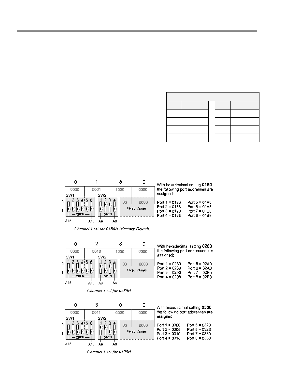
Addressing
The COM232/8AT uses eight I/O address locations per port. Full 16-bit address decoding allows base
address selections in the range: 0000 to FFFF Hex. Two DIP switches, designated SW1 and SW2, are
used to specify the adapter’s base address as follows:
• SW1 determines the address setting for A15 through A10.
• SW2 determines the address setting for A9 through A6.
The adapter uses the remaining address inputs to determine the channel and register being used.
The address of each port is incremented by a factor of
8 (in hexadecimal code) from the base address. For
this reason, 64 address locations are used, as indicated
by the table at the right. Note that SW1, SW2, and
other component locations can be referenced on the
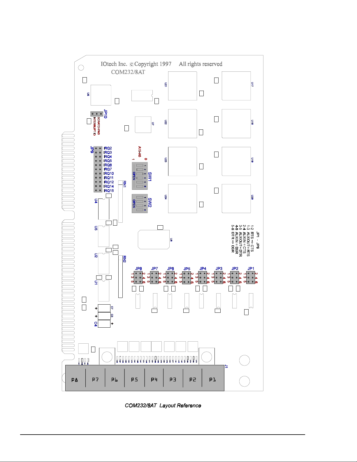
figure, COM232/8AT Layout Reference, on page 6.
Port Range Port Range
10
28
316
424
64 Address Locations
7 5 32
thru
15 6 40
thru
23 7 48
thru
31 8 56
thru
thru
thru
thru
thru
39
47
55
63
The following three figures serve as sample switch settings. Note that there are 6 “hidden” settings,
each with a fixed value of zero. These hidden settings have been included in the following illustrations.
4 COM232/8AT User’s Guide March 1998 1000-0901, rev 1.1
Page 5
Interrupts
The COM232/8AT is capable of supporting 11 interrupt levels (IRQ 2 thru IRQ 7, IRQ 10 thru
IRQ 12, IRQ 14, and IRQ 15). All channels share the same interrupt. You can change the interrupt
selection by repositioning the jumper on JP9. The interrupt positions for JP9 are indicated in the
figure, COM232/8AT Layout Reference, on page 6.
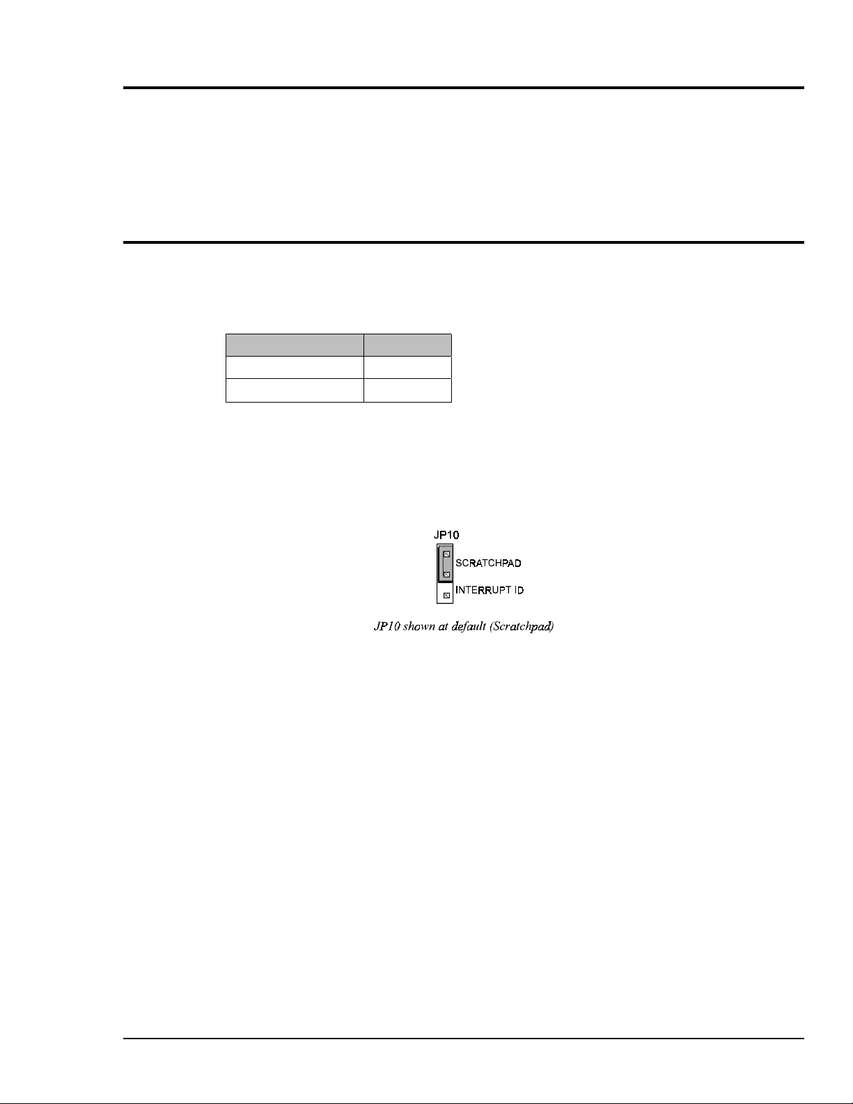
Scratchpad or Interrupt ID Register Selection
Jumper JP10 is used to select the Scratchpad Register, or the Interrupt ID Register. The JP10 setting to
be used is based on the operating system and the software interfacing with the COM232/8AT. The
following table indicates settings for Windows95 and WindowsNT, version 4.0 applications.
System JP10 Setting
Windows95
WindowsNT, version 4.0
Note: The Scratchpad and Interrupt ID registers are discussed in more detail on page 14.
Note: Do not confuse the Interrupt ID Register with the Interrupt Identification Register.
Scratchpad
Interrupt ID
1000-0901, rev 1.1 March 1998 COM232/8AT User’s Guide 5
Page 6
6 COM232/8AT User’s Guide March 1998 1000-0901, rev 1.1
Page 7

Output Configurations
Note: The COM232/8AT board is an RS-232-C DTE (Data Terminal Equipment) device.
RS-232-C Devices
RS-232-C devices are classified according to their function as either Data Terminal Equipment (DTE)
or Data Communication Equipment (DCE). These terms are typically defined as follows:
Data Terminal Equipment (DTE) − A device which serves as the communication source.
Data Communication Equipment (DCE) − A device which provides a channel for communication
between two DTE type devices.
The figure to the right illustrates a basic example of
Data Terminal Equipment (DTE) and Data
Communication Equipment (DCE) making use of
RS-232-C communication links.
As noted above, the COM232/8AT board is an
RS-232-C DTE device. The following figure shows
the layout of the 8-port output connector and includes
the RJ-11 Pinout.
The configuring of AuxIN and AuxOUT is determined by the setting of Jumpers JP1 through JP8, with each jumper
affecting its related port. There are three possible configurations, as indicated in the following examples.
1000-0901, rev 1.1 March 1998 COM232/8AT User’s Guide 7
Page 8

If you need to connect two DTEs together, you must make use of a customized cable known as a NULL MODEM or
MODEM Eliminator. A typical DTE-to-DTE cable is as follows:
Register Definitions
This section provides a brief summary of the 16550 ACE internal registers. The registers are addressed
as indicated in the following table.
Note: The 16550 Asynchronous Communications Element (ACE) enters character mode on reset.
When the 16550 ACE is in character mode it appears as a 16450 ACE to the software.
16550 ACE Internal Register Map
DLAB
(see note)
0 000Receive Buffer (read only)
0 001Interrupt Enable
x 010Interrupt Identification (read only)
x 011Line Control
x 100MODEM Control
x 101Line Status
x 110MODEM Status
x 111Scratch
1 000Divisor Latch (LSB)
1 001Divisor Latch (MSB)
Note: DLAB is accessed through the Line Control Register.
A2 A1 A0 Description
Transmitter Holding Register (write only)
FIFO Control (write only)
Interrupt Enable Register
The bit definitions for the Interrupt Enable Register are as follows:
Interrupt Enable Register Definitions
D7 0
D6 0
D5 0
D4 0
D3 EDSSI MODEM Status
D2 ELSI Receiver Line Status
D1 ETBEI Transmitter Holding Register Empty
D0 ERBFI Received Data Available
8 COM232/8AT User’s Guide March 1998 1000-0901, rev 1.1
Page 9

EDSSI MODEM Status Interrupt − When set (logic 1), enables interrupt on Clear To Send, Data Set
Ready, Ring Indicator, and Data Carrier Detect.
ELSI Receiver Line Status Interrupt − When set (logic 1), enables interrupt on Overrun, Parity,
Framing Errors, and Break Indication.
ETBEI Transmitter Holding Register Empty Interrupt − When set (logic 1), enables interrupt on
Transmitter Register Empty.
ERBFI Received Data Available Interrupt − When set (logic 1), enables interrupt on Received Data
Available. FIFO Mode − When set (logic 1), enables interrupt when the receive FIFO trigger level is
reached. See the FIFO control register for trigger level selections.
Interrupt Identification Register
Note: Do not confuse this register with the Interrupt ID Register.
The bit definitions for the Interrupt Identification Register are as follows:
Interrupt Identification Register Definitions
D7 FFE FIFO Enable (FIFO only)
D6 0
D5 0
D4 0
D3 IID2 IID0, IID1 & IID2 are Interrupt Identifications
D2 IID1
D1 IID0
D0 IP Interrupt Pending
FFE FIFO Enable − When logic 1, indicates FIFO mode is enabled.
IID0, IID1, & IID2 Interrupt Identifications − Indicates highest priority interrupt pending, if any. See
IP (Interrupt Pending) as well as the following table regarding bit definitions. Note that IID2 is always
logic 0 in the 16550 character mode.
IP Interrupt Pending − When logic 0, indicates that an interrupt is pending and that the contents of the
interrupt identification register may be used to determine the source of the interrupt. See IID0, IID1,
IID2, as well as the following table.
Bit Definitions for Interrupt Identifications
IID2 IID1 IID0 IP Priority Interrupt Type
xxx1N/A None.
0 1 1 0 Highest Receiver Line Status
0 1 0 0 Second Received Data Ready
1 1 0 0 Second Character Timeout (FIFO Mode only)
0 0 1 0 Third Transmitting Holding Register Empty
0000FourthMODEM Status
Receiver Line Status − Indicates overrun, parity, framing errors or break interrupts. The interrupt is
cleared by reading the line status register.
Received Data Ready − Indicates receiver data available. The interrupt is cleared by reading the
receiver buffer register. FIFO Mode − Indicates the receiver FIFO trigger level has been reached.
The interrupt is reset when the FIFO drops below the trigger level.
1000-0901, rev 1.1 March 1998 COM232/8AT User’s Guide 9
Page 10

Character Timeout (FIFO Mode only) − Indicates no characters have been removed from, or input to
the receiver FIFO for the last four character times and that there is at least one character in the FIFO
during this time. The interrupt is cleared by reading the receiver FIFO.
Transmitter Holding Register Empty − Indicates that the transmitter holding register is empty. The
interrupt is cleared by reading the interrupt identification register, or by writing to the transmitter
holding register.
MODEM Status − Indicates Clear To Send, Data Set Ready, Ring Indicator, or Data Carrier Detect
have changed state. The interrupt is cleared when the MODEM Status Register is read.
FIFO Control Register
The bit definitions for the FIFO Control Register are as follows:
FIFO Control Register Definitions
D7 RXT1 RXT0 and RXT1 are Receiver Trigger Levels
D6 RXT0
D5 x
D4 x
D3 DMAM DMA Mode Select
D2 XRST Transmit FIFO Reset
D1 RRST Receive FIFO Reset
D0 FE FIFO Enable
RXT0 & RXT1 Receiver FIFO Trigger Levels − Determines the trigger level for the FIFO interrupt as
indicated in the following table.
FIFO Trigger Levels
RXT1 RXT0 Trigger Level
(bytes)
00 1
00 4
10 8
11 14
DMAM DMA Mode Select − Selects the mode of the RxRDY and TxRDY outputs. Note that the
DMA mode is not supported on the RW-100T.
XRST Transmit FIFO Reset − When set (logic 1), all bytes in the transmitter FIFO are cleared and the
counter is reset. The shift register is not cleared. XRST is self-clearing.
RRST Receive FIFO Reset − When set (logic 1), all bytes in receiver FIFO are cleared and the counter
is reset. The shift register is not cleared. RRST is self-clearing.
FE FIFO Enable − When set (logic 1), enables transmitter and receiver FIFOs. When cleared
(logic 0), all bytes in both FIFOs are cleared. This bit must be set when other bits in the FIFO control
register are written to, otherwise the bits will be ignored.
10 COM232/8AT User’s Guide March 1998 1000-0901, rev 1.1
Page 11

Line Control Register
The bit definitions for the Line Control Register are as follows:
Line Control Register Definitions
D7 DLAB Divisor Latch Access Bit
D6 BKCN Break Control
D5 STKP Stick Parity
D4 EPS Even Parity Select
D3 PEN Parity Enable
D2 STB Number of Stop Bits
D1 WLS1 Word Length Select 1
D0 WLS0 Word Length Select 0
DLAB Divisor Latch Access Bit − DLAB must be set to logic 1 to access the baud rate divisor latches.
DLAB must be set to logic 0 to access the receiver buffer, transmitting holding register, and interrupt
enable register.
BKCN Break Control − When set (logic 1), the serial output (SOUT) is forced to the spacing state
(logic 0).
STKP Stick Parity Select − Forces parity to logic 1 or logic 0 if parity is enabled. Also see EPS, PEN,
and the following Parity Selections table.
EPS Even Parity Select − Selects even or odd parity if parity is enabled. Also see STKP, PEN, and the
following Parity Selections table.
PEN Parity Enable − Enables Parity on transmission and verification upon reception. Also see EPS,
STKP, and the following Parity Selections table.
Parity Selections
STKP EPS PEN Parity
xx0None
001Odd
011Even
101Logic 1
111Logic 2
STB Number of Stop Bits − Sets the number of stop bits transmitted. Also see the following WLS1 &
WLS0 text and related Word Length table.
WLS1 & WLS0 Word Length Selects − Determines the number of bits per transmitted word. Also
refer to STB and the following table.
Word Length & Stop Bit Selections
STB WLS1 WLS0 Word Length Stop Bits
0 0 0 5 bits 1
0 0 1 6 bits 1
0 1 0 7 bits 1
0 1 1 8 bits 1
1 0 0 5 bits 1-1/2
1 0 1 6 bits 2
1 1 0 7 bits 2
1 1 1 8 bits 2
1000-0901, rev 1.1 March 1998 COM232/8AT User’s Guide 11
Page 12

MODEM Control Register
The bit definitions for the MODEM Control Register are as follows:
MODEM Control Register Definitions
D7 0
D6 0
D5 0
D4 LOOP Loopback Enable
D3 OUT2 Output 2
D2 OUT1 Output 1
D1 RTS Request to Send
D0 DTR Data Terminal Ready
LOOP Loopback Enable − When set (logic 1), the transmitter shift register is connected directly to the
receiver shift register. The MODEM control inputs are internally connected to the MODEM control
outputs and the outputs are force to the inactive state. For this reason all transmitted characters are
immediately received to verify the transmit and receive data paths. Note that the transmitter and
receiver interrupts still undergo normal operation. MODEM control interrupts are available, but are
now controlled through the MODEM Control Register.
Note: Bits OUT2, OUT1, RTS, and DTR (described below) perform identical functions on their
respective outputs. In each case, when the bit is set (logic 1) in the register, the associated
output is forced to logic 0. When cleared (logic 0), the associated output is forced to logic 1.
OUT2 Output 2 − Controls the OUT2 output [pin 31] as described in the above note.
OUT1 Output 1 − Controls the OUT1 output [pin 34] as described in the above note.
RTS Request To Send − Controls the RTS output [pin 32] as described in the above note.
DTR Data Terminal Ready − Controls the DTR output [pin 33] as described in the above note.
12 COM232/8AT User’s Guide March 1998 1000-0901, rev 1.1
Page 13

Line Status Register
The bit definitions for the Line Status Register are as follows:
Line Status Register Definitions
D7 FFRX Error in FIFO RCVR (FIFO only)
D6 TEMT Transmitter Empty
D5 THRE Transmitter Holding Register Empty
D4 BI Break Interrupt
D3 FE Framing Error
D2 PE Parity Error
D1 OE Overrun Error
D0 DR Data Ready
FFRX FIFO Receiver Error − Always logic 0 when in the 16550 character mode. FIFO Mode −
Indicates one or more parity errors, framing errors, or breaks in the receiver FIFO. FFRX is reset by
reading the Line Status Register.
TEMT Transmitter Empty − Indicates the transmitter holding register (or FIFO) and the transmitter
shift register are empty and are ready to receive new data. TEMT is reset by writing a character to the
Transmitter Holding Register.
THRE Transmitter Holding Register Empty − Indicates the Transmitter Holding Register (or FIFO) is
empty and is ready to accept new data. THRE is reset by writing data to the Transmitter Holding
Register.
Note: This note pertains to the bits BI, FE, PE, and OE. These bits are sources of receiver line
status interrupts. The bits are reset by reading the Line Status Register. In FIFO mode, each
bit is associated with a specific character in the FIFO and the exception is revealed only when
that character reaches the top of the FIFO.
BI Break Interrupt − Indicates the received data input has been in the spacing state (logic 0) for longer
than the transmission time of one full word. FIFO Mode − Only one zero character is loaded into the
FIFO and transfers are disabled until SIN goes to the mark state (logic 1) and a valid start bit is
received.
FE Framing Error − Indicates the received character had an invalid stop bit. The stop bit following
the last data or parity bit was a 0 bit (spacing level).
PE Parity Error − Indicates the received data does not have the correct parity.
QE Overrun Error − Indicates the receive buffer was not read before the next character was received.
The character is destroyed. FIFO Mode − Indicates the FIFO is full and another character has been
shifted in. The character in the shift register is destroyed, but is not transferred to the FIFO.
DR Data Ready − Indicates data is present in the receive buffer (or FIFO). DR is reset by reading the
Receive Buffer Register.
1000-0901, rev 1.1 March 1998 COM232/8AT User’s Guide 13
Page 14

MODEM Status Register
The bit definitions for MODEM Status Register are as follows:
MODEM Status Register Definitions
D7 DCD Data Carrier Detect
D6 RI Ring Indicator
D5 DSR Data Set Ready
D4 CTS Clear To Send
D3 DDCD Delta Data Carrier Detect
D2 TERI Trailing Edge Ring Indicator
D1 DDSR Delta Data Set Ready
D0 DCTS Data Clear To Send
DCD Data Carrier Detect − Complement of the DCD input, pin 38.
RI Ring Indicator − Complement of the RI input, pin 39.
DSR Data Set Ready − Complement of the DSR input, pin 37.
CTS Cleat To Send − Complement of the CTS input, pin 36.
Note: This note pertains to the bits DDCD, TERI, DDSR, and DCTS. These bits are the sources of
the MODEM Status Interrupts. These bits are reset when the MODEM Status Interrupt is
read.
DDCD Delta Data Carrier Detect − Indicates the Data Carrier Detect (DCD) input [pin 38] has
changed state.
TERI Trailing Edge Ring Indicator − Indicates the Ring Indicator (RI) input [pin 39] has changed
from a low state to a high state.
DDSR Delta Data Set Ready − Indicates the Data Set Ready (DSR) input [pin 37] has changed state.
DCTS Delta Clear To Send − Indicates the Clear To Send (CTS) input [pin 36] has changed state−
Indicates the FIFO is full and another character has been shifted in. The character in the shift register is
destroyed, but is not transferred to the FIFO.
Scratchpad Register (Interrupt ID Register not accessible)
Each 16550 ACE (Asynchronous Communication Element) has a Scratchpad Register at Base+7. The
Scratchpad Register is a read/write register which is not used by the 16550 ACE to perform
communication transfers. However, you can use the Scratchpad Register for general purpose data
storage. The Scratchpad Register is selected by positioning the jumper on JP10 to pins 1 and 2. The
location of JP10 is shown on page 6.
Note: The JP10 jumper should be positioned to Scratchpad for Windows95 applications.
Interrupt ID Register (Scratchpad Register not accessible)
Note: Do not confuse this register with the Interrupt Identification Register.
The Interrupt ID Register is accessed by reading Base+7 of any 16550 ACE. This
returns the interrupt status of all eight ACEs. IPX indicates Interrupt Pending on
the associated channel. The Interrupt ID Register is selected by positioning the
jumper on JP10 to pins 2 and 3. The location of JP10 is shown on page 6.
Note: The JP10 jumper should be positioned to ID Interrupt for
WindowsNT version 4.0 applications.
D7
IP8
D6
IP7
D5
IP6
D4
IP5
D3
IP4
D2
IP3
D1
IP2
D0
IP1
Interrupt ID Register
14 COM232/8AT User’s Guide March 1998 1000-0901, rev 1.1
Page 15

FIFO Interrupt Mode Operation
When the receiver FIFO and receiver interrupts are enabled, interrupts will occur as follows:
1. The Received Data Available Interrupt (ERBFI) will be issued to the CPU when the FIFO reaches
the programmed trigger level. This interrupt will be cleared as soon as the FIFO falls below its
programmed trigger level.
2. The Interrupt Identification Register’s (IIR) receive data available indicator is set and cleared
along with the Received Data Available Interrupt (see 1 above).
3. The Data Ready (DR) indicator is set as soon as a character is transferred into the receiver FIFO.
The DR indicator is cleared when the FIFO is empty.
Divisor Latch Settings for Common Baud Rates
The following table lists divisor latch settings for common baud rates using a 1.8432 MHz input clock.
Desired
Baud Rate
Divisor Latch Settings for Common Baud Rates
Divisor
Latch Value
Error
2
Desired
Baud Rate
Latch Value
Divisor
1
2
Error
50 2304 --- 2400 48 ---
75 1536 --- 3600 32 ---
110 1047 0.026 4800 24 ---
150 768 -- 7200 16 ---
300 384 --- 9600 12 ---
600 192 --- 19200 6 ---
1200 96 --- 38400 3 ---
1800 64 --- 56000 2 2.86
2000 58 0.69 --- --- ---
Note 1: Input clock used is 1.8432 MHz.
Note 2: Error is the error between “Desired” and “Actual” baud rate value.
1000-0901, rev 1.1 March 1998 COM232/8AT User’s Guide 15
Page 16

Installation for Windows95
TM
Before Installing the COM232/8AT Board:
1. On the COM232/8AT board, ensure jumper JP10 is in its Scratchpad default (pins 1 and 2
jumpered).
2. Ensure correct base I/O address is set on switches SW1 and SW2.
3. Ensure IRQ is properly set on jumper JP9.
4. Turn PC Power Off, and unplug computer system.
Installing the COM232/8AT Board
1. Ensure PC Power is Off, and system is unplugged.
2. Remove PC cover as instructed by your computer reference guide.
3. Carefully insert the COM232/8AT board into a vacant slot. Consult your computer reference
guide if needed.
4. Replace computer cover.
5. Re-apply power to your computer system.
Installing COM232AT.inf
An information file must be installed for Windows95 systems. The required file resides on a 3.5” disk
that has been provided with your order. After your COM232/8AT card has been installed, insert the
information disk in your computer’s 3.5” drive and install the .inf file per the following ten steps.
Note: A screen montage has been included on page 17. The circled numbers in the montage
correspond to the following ten steps.
1. Activate Windows95 Desktop Start menu.
2. Select Settings.
3. Select Control Panel.
4. Select Add New Hardware. The Add New Hardware Wizard appears.
5. Select Next >.
6. Select (
hardware?”
7. Select Next >. The Hardware types list appears.
8. Select Other devices.
9. Select Next >.
10. Select Have Disk …
) No. This is in response to the statement, “Do you want Windows to search for your new
••••
16 COM232/8AT User’s Guide March 1998 1000-0901, rev 1.1
Page 17

The .inf file will now install. When the installation is complete, your COM232/8AT will be listed as hardware
types in System Devices and Ports (COM & LPT), located in the Add New Hardware Wizard.
Steps Required to Install Com232AT.inf Information File
(For Windows95 Only)
This completes the installation of COM232/8AT for Windows95.
1000-0901, rev 1.1 March 1998 COM232/8AT User’s Guide 17
Page 18

Installation for WindowsNTTM Version 4.0 Only
If your application makes use of WindowsNT 4.0 use the following steps to install COM232/8AT.
Note: The following procedure does not
Before Installing the COM232/8AT Board:
1. On the COM232/8AT board, ensure jumper JP10 is set for Interrupt ID (pins 2 and 3 jumpered).
2. Ensure correct base I/O address is set on switches SW1 and SW2. Make note of I/O address for
later use.
3. Ensure IRQ is properly set on jumper JP9. Make note of IRQ for later use.
4. Turn PC Power Off, and unplug computer system.
Installing the COM232/8AT Board
1. Ensure PC Power is Off, and system is unplugged.
2. Remove PC cover as instructed by your computer reference guide.
3. Carefully insert the COM232/8AT board into a vacant slot. Consult your computer reference
guide if needed.
4. Replace computer cover.
5. Re-apply power to your computer system.
Adding COM Ports
1. From the WindowsNT 4.0 Start Menu, select Settings.
2. Select Control Panel.
3. Select Ports. The currently installed ports are displayed.
4. Select Add. This permits you to add on the next available COM port.
5. Select (or key in) base I/O Address (as noted before installing the board).
6. Select IRQ.
7. Verify FIFO Enabled is checked. If not, check FIFO Enabled.
8. Perform the following three steps for each additional port to be added:
a) Select Add. This permits you to add the next available COM port.
b) Select (or key in) the next available I/O Address.
Note: The address of each port is incremented by a factor of 8 (in hexadecimal code) from the base
address. Addressing information is contained on page 4 of this manual.
c)
Select the IRQ (same IRQ as entered in step 6 above).
make use of an installation disk.
Entering COM Port Settings
1. Restart the PC.
2. Select Settings from the WindowsNT 4.0 Start Menu.
3. Select Control Panel.
4. Select Ports.
5. Select the ports Settings button.
6. Set the following Com port parameters [for each port] according to your application:
Data Bits, Parity, Stop Bits, Flow Control (Handshake).
7.
Restart the PC.
This completes the installation of COM232/8AT for WindowsNT 4.0.
18 COM232/8AT User’s Guide March 1998 1000-0901, rev 1.1
Page 19

−
User Notes
1000-0901, rev 1.1 March 1998 COM232/8AT User’s Guide 19
Page 20

20 COM232/8AT User’s Guide March 1998 1000-0901, rev 1.1
 Loading...