

Page 1

CIO-QUAD02
CIO-QUAD04
2 & 4 Channel Quadrature
Encoder Input Boards
User’s Manual
Revision 2
December, 2000
Page 2

LIFETIME WARRANTY
Every hardware product manufactured by Measurement Computing Corp. is warranted against defects in materials or
workmanship for the life of the product, to the original purchaser. Any products found to be defective will be repaired or
replaced promptly.
LIFETIME HARSH ENVIRONMENT WARRANTY
Any Measurement Computing Corp. product which is damaged due to misuse may be replaced for only 50% of the
current price. I/O boards face some harsh environments, some harsher than the boards are designed to withstand. When
that happens, just return the board with an order for its replacement at only 50% of the list price. Measurement
Computing Corp. does not need to pro fit from your misfortune. By the way, we will honor this warranty for any other
manufacture’s board that we have a replacement for!
30 DAY MONEY-BACK GUARANTEE
Any Measurement Computing Corp. product may be returned within 30 days of purchase for a full refund of the price
paid for the product being returned. If you are not satisfied, or chose the wrong product by mistake, you do not have to
keep it. Please call for a RMA number first. No credits or returns accepted without a copy of the original invoice. Some
software products are subject to a repackaging fee.
These warranties are in lieu of all other warranties, expressed or implied, including any implied warranty of
merchantability or fitness for a particular application. The remedies provided herein are the buyer’s sole and exclusive
remedies. Neither Measurement Computing Corp., nor its employees shall be liable for any direct or indirect, special,
incidental or consequential damage arising from the use of its products, even if Measurement Computing Corp. has
been notified in advance of the possibility of such damages.
MEGA-FIFO, the CIO prefix to data acquisition board model numbers, the PCM prefix to data acquisition boa rd model
numbers, PCM-DAS08, PCM-D24C3, PCM-DAC02, PCM-COM422, PCM-COM485, PCM-DMM,
PCM-DAS16D/12, PCM-DAS16S/12, PCM-DAS16D/16, PCM-DAS16S/16, PCI-DAS6402/16, Universal Library,
InstaCal, Ha rsh Environment Warran ty and Measurement Computing Corp. are registered trademarks of Measurement
Computing Corp.
IBM, PC, and PC/AT are trademarks of International Business Machines Corp. Windows is a trademark of Microsoft
Corp. All other trademarks are the property of their respective owners.
Information furnished by Measurement Computing Corp. is believed to be accurate and reliable. However, no
responsibility is assumed by Measurement Computing Corp. neither for its use; nor for any infringements of patents or
other rights of third parties, which may result from its use. No license is granted by implication or otherwise under any
patent or copyrights of Measurement Computing Corp.
All rights reserved. No part of this publication may be reproduced, sto red in a retrieval system, or transmitted, in any
form by any means, electronic, mechanical, by photocopying, recording or otherwise without the prior written
permission of Measurement Computing Corp.
TM
Notice
Measurement Computing Corp. does not authorize any Measurement Computing Corp. product for
use in life support systems and/or devices without the written approval of the President of
Measurement Computing Corp. Life support devices/systems are devices or systems which, a) are
intended for surgical implantation into the body, or b) support or sustain life and whose failure to
perform can be reasonably expected to result in injury. Measurement Computing Corp. products are
not designed with the components required, and are not subject to the testing required to ensure a
level of reliability suitable for the treatment and diagnosis of people.
HM CIO-QUAD0#.lwp
Copyright 2000, Measurement Computing Corp.
©
Page 3

Table of Contents
1 INTRODUCTION
2 INSTALLATION
3 CIO-QUAD CONNECTOR DIAGRAM
4 REGISTER MAP AND DESCRIPTIONS
5 ELECTRICAL SPECIFICATIONS
..........................................................................
..........................................................................
..........................................................
.......................................................
......................................................
1
11.1 QUADRATURE ENCODERS AND THE CIO-QUAD .........................................
3
32.1 SOFTWARE ...........................................................................
32.2 HARDWARE ..........................................................................
32.2.1 Base Address Switch .................................................................
32.2.2 Interrupt Level Select ................................................................
32.2.3 Single-Ended/Differential Switch and Jumper Settings ......................................
42.2.4 Termination Resistors ................................................................
42.3 PLUG IN THE CIO-QUAD BOARD ........................................................
52.4 TESTING THE INSTALLATION ..........................................................
52.4.1 InstaCAL ..........................................................................
52.4.2 QUAD Encoder Demo Software .......................................................
5
6
64.1 OVERVIEW ...........................................................................
74.2 CHANNEL CONTROL REGISTERS (Base + 0 through Base + 7) ................................
74.2.1 Base +0, 2, 4 and 6 : Output Latch and Preset Registers .....................................
74.2.2 Base +1, 3, 5 and 7: FLAG, RLD, CMR, IOR and IDR Registers .............................
114.3 GLOBAL CONTROL REGISTERS (Base +8 through Base +12) ................................
114.3.1 Base +8: Index & Interrupt Routing Control Register ......................................
124.3.2 Base +9: Input Signal Control Register .................................................
124.3.3 Base +10 and 11: Programmable Interrupt Controller Registers ..............................
124.3.4 Base +12: Interrupt Select Register ....................................................
13
Page 4

This page is blank.
Page 5

1 INTRODUCTION
The CIO-QUAD02 is an ISA plug-in board that provides inputs and decoding for one or two incremental quadrature
encoders. A four channel version, the CIO-QUAD04, provides inputs and decoding for up to four encoders. Either the
CIO-QUAD02 or 04 can also be used as a high speed pulse counter for general counting applications.
PLEASE NOTE: If you have a CIO-QUAD04, all instructions in this manual apply. If you have a CIO-QUAD02, you
should ignore all references to channels 3 and 4. In all other respects, the two models are identical. In this manual, we will
refer to both boards generically as CIO-QUAD.
1.1 QUADRATURE ENCODERS AND THE CIO-QUAD
Incremental quadrature encoders are used to provide feedback signals from motors, that is, to count rotations and convert
the physical movement into a series of electrical signals. These signals are sent to the computer which then decides whether
or not to trigger signals that control the motor’s movement and what those control signals should be. The Measurement
Computing Corp. CIO-QUAD is the link between incremental quadrature encoders and the computer.
The CIO-QUAD is a plug-in board for PC/XT/AT computers; it uses one ISA slot and one rear panel opening for up to 2
channels (CIO-QUAD02) or one ISA slot and two rear panel openings for up to four channels (CIO-QUAD04). Each
incremental quadrature encoder connects to an input channel o n the CIO-QUAD through a DB9 female connector on the
board’s rear panel. Channels 1 and 2 connect to the DB9 connectors attached directly to the board. Channels 3 and 4
(CIO-QUAD04) connect to the DB9 connectors on an auxiliary rear panel bracket.
For each channel, the signals at the DB9 connectors are:
y
Phase A+, A-
y
Phase B+, B-
y
Index +/-
y
+5 and GND (optional power for +5V encoders)
For pinout diagrams refer to Section 2.3.
The CIO-QUAD board provides inputs for three basic signals, Phase A, Phase B, and Index. Phase A and Phase B are
generated at a 90° phase shift with respect to each other. Using these signals, a computer with a CIO-QUAD can determine
system position (counts), velocity, (counts per second), and direction of rotation.
The Index signal is used to establish an absolute reference position within one count of the encoder rotation (360°).
Therefore, the Index signal is often used to reset o r preset the position counter, particularly upon system startup when the
incremental encoder cannot determine the starting position of the motor. The Index signal can also be used to generate an
interrupt signal to the computer.
The Phase A, Phase B, and Index inputs are jumper-selectable for differential or single-ended input. These signals, after
being routed through differential receiver s, offer various paths to the LS7266 inputs through the FPGA. The inputs a re
register-selectable for:
y
individual incremental encoder inputs to allow up to four channels
y
cascadable counters to allow non-quadrature counting up to 96-bits
y
routing the Index input to either the Load Counter/Load Latch input or the Reset Counter/Gate input with quarter cycle
and half cycle signals supported
y
routing the Compare or Carry/Borrow output signals to the 8259 Interrupt controller
The heart of the CIO-QUAD is the LSI Computer Systems, Inc., LS7266R1 24-bit Dual Axis Quadrature Counter chip.
1
Page 6
This component contains:
y
two, 24-bit counters
y
associated 24-bit preset and 24-bit output latch registers
y
integrated digital filtering with 8-bit counter prescalers
It provides:
y
programmable index functionality
y
programmable count modes including non-quadrature modes.
y
CIO-QUAD can also operate as a high-speed pulse and general purpose counter, cascadable to 96 bits. The 24-bit
counter can count either in binary or BCD through register selection.
The CIO-QUAD also includes an 8259 Programmable Interrupt Controller which accepts the four Index inputs directly and
the Carry/Borrow outputs from the LS7266 (counter overflow/underflow or count value match) to generate interrupts to the
PC bus. The interrupt controller operates in Polled Mode and allows for masking and priority setting of the interrupt inputs.
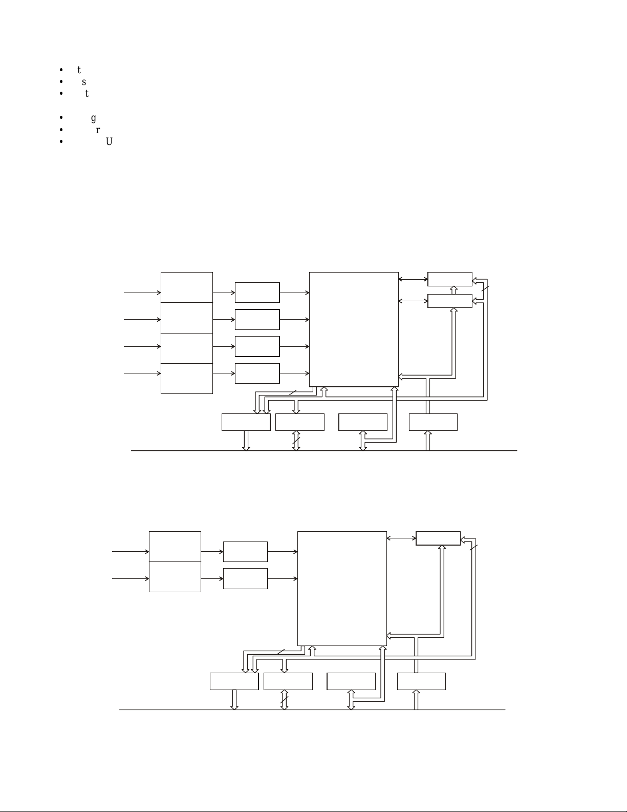
For an overall view of CIO-QUAD functionality, see the block diagrams in Figure 1-1 below.
CIO-QUAD04
QUADRATURE
ENCODER
INPUT
QUADRATURE
ENCODER
INPUT
Channel 1
Channel 2
Channel 1
Channel 2
Channel 3
Channel 4
S.E./Diff.
Setting
Termination
S.E./Diff.
Setting
Termination
S.E./Diff.
Setting
Termination
S.E./Diff.
Setting
Termination
S.E./Diff.
Setting
Termination
S.E./Diff.
Setting
Termination
75ALS175
75ALS175
75ALS175
75ALS175
8259 PIC
75ALS175
75ALS175
INTERRUPT
IRQ’S
Signal Routing
8
DATA
TRANSCEIVER
8
DATA
ISA-BUS
CIO-QUAD02
Control
Signal Routing
Control
Decode
FPGA
Decode
FPGA
ADDRESS
DECODER
LS7266: 24-Bit Dual-Axis
Quadrature Counter
Channels
Signalling
Signalling
CONTROL
ADDRESS
LS7266: 24-Bit Dual-Axis
Quadrature Counter
Signalling
1&2
Channels
3&4
BUFFER
CONTROL
Channels
1&2
DATA BUS
DATA BUS
INTERRUPT
8259 PIC
IRQ’S
8
DATA
TRANSCEIVER
8
DATA
ISA-BUS
ADDRESS
DECODER
Figure 1-1. Functional Block Diagrams
2
ADDRESS
CONTROL
BUFFER
CONTROL
Page 7

2.1 SOFTWARE
2 INSTALLATION
The board has a variety of switches and jumpers to set before installing the board in your computer. The simplest way to
configure your boar d is to use the
Insta
TM
program provided on the CD (or floppy disk).
Cal
Insta
Cal will show you all
available options, how to configure the various switches and jumpers to match your application requirements, and will
create a configuration file that your application software (and the Universal Library) will refer to so the software you use
will automatically have access to the exact configuration of the board.
Please refer to the
Software Installation Manual
regarding the installation and operatio n of
Insta
Cal. The following hard
copy information is provided as a matter of completeness, and will allow you to set the hardware configuration of the board
if you do not have immediate access to
Insta
Cal and/or your computer.
2.2 HARDWARE
The CIO-QUAD02 has a set Base Address switches, and a bank of six switches and six jumpers for setting the quadrature
inputs for differential or single-ended modes. The CIO-QUAD04 has Base Address switches and two banks of switches (six
each) and 12 jumpers to set the quadrature inputs for differential or single-ended modes.
2.2.1 Base Address Switch
Prior to installing the CIO-QUAD board s, set the base address by using the dip switch located on the bo ard. Use the base
address switch description below to guide your base address selection.
Unless there is already another board in your system using address 300h (768 decimal), you can leave the switches as they
are set at the factory. The example shown in Figure 2-1 shows the settings for the factory default base address of 300h.
9876
5
4
SW
A9
A8
A7
A6
A5
A4
HEX
200
100
80
40
20
10
BASE ADDRESS SW ITCH
- Address 300H shown here.
Figure 2-1. Base Address Switch
A complete address is constructed by calculating the hex or decimal number which corresponds to the address that the
CIO-QUAD will respond to. In the default configuration, shown above, addresses 9 and 8 are DOWN, and all others are
UP. Address 9 = 200h (512 decimal) and address 8 = 100h (256 decimal). When added together they equal 300h (768
decimal).
2.2.2 Interrupt Level Select
The interrupt level used by the CIO-QUAD board is selected in software. They are most easily set in InstaCAL, and are then
saved to the .CFG file that the Universal Library and some third party software use to determine the current board
configuration. Please refer to chapter 4 for details regarding setting the Interrupt level via register level programming.
2.2.3 Single-Ended/Differential Switch and Jumper Settings
Prior to installation, set the switches and jumpers on the CIO-QUAD to the settings required by your application. The board
is supplied preset for single-ended use with no termination resistors installed. This section gives you the information
necessary to change the defaults (all switches ON (up) and jumpers on pins 2 and 3).
3
Page 8

Differential Configuration
Insert Jumpers From pin 1 to 2
Set Switch to OFF (down)
Single-Ended Configuration
Insert Jumpers From pin 2 to 3
Set Switch to S2 (and S3) ON (up)
Chan 4Chan 3Chan 2Chan 1Input
W25W22W19W16Phase A
W26W23W20W17Phase B
W27W24W21W18Index
Chan 4Chan 3Chan 2Chan 1Input
S3-4S3-1S2-4S2-1Phase A
S3-5S3-2S2-5S2-2Phase B
S3-6S3-3S2-6S2-3Index
Chan 4Chan 3Chan 2Chan 1Input
W25W22W19W16Phase A
W26W23W20W17Phase B
W27W24W21W18Index
Chan 4Chan 3Chan 2Chan 1Input
S3-4S3-1S2-4S2-1Phase A
S3-5S3-2S2-5S2-2Phase B
S3-6S3-3S2-6S2-3Index
2.2.4 Termination Resistors
Although termination resistors are not typically required, plated-through holes on the board have been left open and labeled
to allow the user to install resistors across the various inputs.
Install Termination Resistors
Chan 4Chan 3Chan 2Chan 1Input
R31,32R25,26R19,20R13,14Phase A
R33,34R27,28R21,22R15,16Phase B
R35, 36R29, 30R23, 24R17, 18Index
2.3 PLUG IN THE CIO-QUAD BOARD
1. After selecting a nd ver ifying the base add ress, and setting the co nfiguration switches and j umpers, shut the co mputer off
and open the case.
2. Locate an empty expansion slot in your computer. The CIO-QUAD02 board requires a single 16-bit slot (with two
connectors). The CIO-QUAD04 requires an open slot as well as an adjacent open rear panel opening.
3. Push the board firmly down into the expansion b us connector . If it is not seated fully it may fail to work and could short
circuit the PC bus power onto a PC bus signal. This could damage the motherboard in your PC as well as the CIO-QUAD
board.
4. Secure the board in the ISA slot with the screw provided.
5. You may also wish to connect your cable, screw terminal board or other field wiring at this time.
6. Replace the cover to the computer and turn it on.
4
Page 9

2.4 TESTING THE INSTALLATION
2.4.1 InstaCAL
Run the
the base address has been properly set and the onboard registers are performing as expected. If the test fails, try
reconfiguring the board with a different Base Address. Once the board has been tested, select
configuration file will be written to your hard disk.
Insta
Cal program to test your board. Select the "Test" function o f InstaCAL. This will run an internal test to assure
FILE
then
Exit
, and the
2.4.2 QUAD Encoder Demo Software
Included with your CIO-QUAD board is a floppy disk labeled QUAD ENCODER DEMO SOFTWARE. This disk contains
a demo program that allows you use many of the features of the CIO-QUAD without writing any code.
To install the demo software, insert the disk and run the SETUP .EXE pr ogram. Once installed, j ust do uble click the icon in
the QUADENC program group to run the program. You will be prompted to enter the board type and the base address you
selected above. Click OK after entering the appropriate values.
The main program screen allows to select the channels you wish to read and many configuration options for those channels.
3 CIO-QUAD CONNECTOR DIAGRAM
Pin assignments for both differential and single-ended connections are shown in Figure 3-1 below.
phase the encoder according to the manufacturer’s instructions.
Phase A- 1
+5V 2
Phase B- 3
+5V 4
In dex - 5
6 P has e A+
7 P has e B+
8 GND
9 Index+
Differential
Viewed from the outs ide of the computer looking into the connectors on the board
Figure 3-1. Connector Pin Outs for CIO-QUAD04
GND 1
+5V 2
GND 3
+5V 4
GND 5
S ingle-Ended
6 P has e A+
7 P has e B+
8 Ground
9 Index+
Viewed from above
Be sure to properly
5
Page 10

4 REGISTER MAP AND DESCRIPTIONS
-
-
-
*--------- ----- SEE LS7266R1 S PEC -----------------
*--------- ----- SEE LS7266R1 S PEC -----------------
-
-
-
-
-
*--------- ----- SEE LS7266R1 S PEC -----------------
*--------- ----- SEE LS7266R1 S PEC -----------------
*--------- ----- SEE LS7266R1 S PEC -----------------
-
-
-
-
-
*--------- ----- SEE LS7266R1 S PEC -----------------
*--------- ----- SEE LS7266R1 S PEC -----------------
*--------- ----- SEE LS7266R1 S PEC -----------------
-
-
-
-
-
*--------- ----- SEE LS7266R1 S PEC -----------------
*--------- ----- SEE LS7266R1 S PEC -----------------
*--------- ----- SEE LS7266R1 S PEC -----------------
-
-
-
-
*--------- ----------- 8259 Pro gra mmab le In terrupt C ontroller Po rt B --------------------
4.1 OVERVIEW
The following section tabulates the register map of the CIO-QUAD series and briefly describes the commands necessary to
program the CIO-QUAD at the register level. The heart of the board is the LSI/CSI LS7266R1, a powerful device which is
highly integrated, requiring fewer external components. As seen in the LS7266R1 block diagram, many functions are
controlled through register programming. Refer to the register map in Table 4-1 below and the following descriptions.
Table 4-1. Register Map
Register Data Bits
Base + 0RDD7D6D5D4D3D2D1D0Read Channel 1 OL byte segment addressed by BP
Base + 1 RD 0 I DX U/D* E S CPT CT BT Read Chan nel 1 FLAG register
Base + 2RDD7D6D5D4D3D2D1D0Read Channel 2 OL byte segment addressed by BP
Base + 3 RD 0 I DX U/D* E S CPT CT BT Read Chan nel 2 FLAG register
Base + 4RDD7D6D5D4D3D2D1D0Read Channel 3 OL byte segment addressed by BP
Base + 5 RD 0 I DX U/D* E S CPT CT BT Read Chan nel 3 FLAG register
Base + 6RDD7D6D5D4D3D2D1D0Read Channel 4 OL byte segment addressed by BP
Base + 7 RD 0 I DX U/D* E S CPT CT BT Read Chan nel 4 FLAG register
Base + 8 RD CBINT4 CBINT 3 CBINT2 CBINT 1 IND4SE L IND3SE L IND2SE L IND1SE L Interrup t rou ting con trol reg ister
Ba se + 9 RD N/A PH4B1 PH4B0 PH4A PH3B PH3A PH2B PH2 A Inp ut sign al con tro l reg ist er (for c ascading c ount ers)
Base + 1 0 RD *-------------------- 8259 Program ma ble Interrupt Controller Port A -------------------Base + 1 1 RD
Ba se + 12 RD N/ A N/ A N/A N/A INTE INT2 INT1 INT0 Int errupt selec tion reg ister
D7 D6 D5 D4 D3 D2 D1 D0 Fu nctio n
WR D7 D6 D5 D4 D3 D2 D1 D0 Write Chan nel 1 PR b y t e se gment add ressed by BP
WR 0 0 0 *-------------- SEE LS7266R1 SPEC ----------------
WR 0 0 1 *-------------- SEE LS7266R1 SPEC ---------------WR 0 1 0 *-------------- SEE LS7266R1 SPEC ---------------WR 0 1 1
WR 1 0 0
WR 1 0 1 *-------------- SEE LS7266R1 SPEC ---------------WR 1 1 0 *-------------- SEE LS7266R1 SPEC ---------------WR 1 1 1 *-------------- SEE LS7266R1 SPEC ----------------
WR D7 D6 D5 D4 D3 D2 D1 D0 Write Chan nel 2 PR b y t e se gment add ressed by BP
WR 0 0 0 *-------------- SEE LS7266R1 SPEC ----------------
WR 0 0 1 *-------------- SEE LS7266R1 SPEC ---------------WR 0 1 0
WR 0 1 1
WR 1 0 0
WR 1 0 1 *-------------- SEE LS7266R1 SPEC ---------------WR 1 1 0 *-------------- SEE LS7266R1 SPEC ---------------WR 1 1 1 *-------------- SEE LS7266R1 SPEC ----------------
WR D7 D6 D5 D4 D3 D2 D1 D0 Write Chan nel 3 PR b y t e se gment add ressed by BP
WR 0 0 0 *-------------- SEE LS7266R1 SPEC ----------------
WR 0 0 1 *-------------- SEE LS7266R1 SPEC ---------------WR 0 1 0
WR 0 1 1
WR 1 0 0
WR 1 0 1 *-------------- SEE LS7266R1 SPEC ---------------WR 1 1 0 *-------------- SEE LS7266R1 SPEC ---------------WR 1 1 1 *-------------- SEE LS7266R1 SPEC ----------------
WR D7 D6 D5 D4 D3 D2 D1 D0 Write Chan nel 4 PR b y t e se gment add ressed by BP
WR 0 0 0 *-------------- SEE LS7266R1 SPEC ----------------
WR 0 0 1 *-------------- SEE LS7266R1 SPEC ---------------WR 0 1 0
WR 0 1 1
WR 1 0 0
WR 1 0 1 *-------------- SEE LS7266R1 SPEC ---------------WR 1 1 0 *-------------- SEE LS7266R1 SPEC ---------------WR 1 1 1 *-------------- SEE LS7266R1 SPEC ----------------
WR CBINT4 CBINT3 CBINT2 CB INT1 IND4SEL IND3SEL IND2SEL IND1SEL
W R N/A PH4 B1 PH4 B0 PH4A PH3B PH3A PH2 B PH2A
WR *--------- ----------- 8259 Pro gra mmab le In terrupt C ontroller Po rt A -----------------------*
WR *--------- ----------- 8259 Pro gra mmab le In terrupt C ontroller Po rt B -----------------------*
WR N/ A N/A N/ A N/A INTE INT2 INT1 INT0
Writ e to Channe l 1 RLD re giste r
Writ e to Channe l 1 CM R re giste r
Writ e to Channe l 1 IOR registe r
Writ e to Channe l 1 IDR reg ister
Writ e to Channe l 1 and 2 RLD re gister
Writ e to Channe l 1 and 2 CM R re giste r
Writ e to Channe l 1 and 2 IOR registe r
Writ e to Channe l 1 and 2 IDR reg ister
Writ e to Channe l 2 RLD re giste r
Writ e to Channe l 2 CM R re giste r
Writ e to Channe l 2 IOR registe r
Writ e to Channe l 2 IDR reg ister
Writ e to Channe l 1 and 2 RLD re gister
Writ e to Channe l 1 and 2 CM R re giste r
Writ e to Channe l 1 and 2 IOR registe r
Writ e to Channe l 1 and 2 IDR reg ister
Writ e to Channe l 3 RLD re giste r
Writ e to Channe l 3 CM R re giste r
Writ e to Channe l 3 IOR registe r
Writ e to Channe l 3 IDR reg ister
Writ e to Channe l 3 and 4 RLD re gister
Writ e to Channe l 3 and 4 CM R re giste r
Writ e to Channe l 3 and 4 IOR registe r
Writ e to Channe l 3 and 4 IDR reg ister
Writ e to Channe l 4 RLD re giste r
Writ e to Channe l 4 CM R re giste r
Writ e to Channe l 4 IOR registe r
Writ e to Channe l 4 IDR reg ister
Writ e to Channe l 3 and 4 RLD re gister
Writ e to Channe l 3 and 4 CM R re giste r
Writ e to Channe l 3 and 4 IOR registe r
Writ e to Channe l 3 and 4 IDR reg ister
Program ma ble In terrupt Con tro ll er Port A
Program ma ble In terrupt Con tro ll er Port B
6
Page 11

4.2 CHANNEL CONTROL REGISTERS (Base + 0 through Base + 7)
The LS7266R1 contains two control registers per axis, and the configuration of each axis requires a sequence of writes to
set the operating mode of the chip. The following description outlines the configuration steps for a single axis. The first axis
control registers (channel 1) are contained at addresses BASE +0 and BASE+1. The other axis (at BASE +2 & 3, BASE +4
& 5 and BASE + 6 & 7) perform identically.
4.2.1 Base +0, 2, 4 and 6 : Output Latch and Preset Registers
When read, the BASE +0 address returns the Output Latch (OL) data. Writes to the BASE +0 address set the Preset
Register (PR). All register access to the LS7266R1 is done through byte wid e op era tions, however, the PR and OL registe rs
are 24-bits wide. The LS7266R1 contains a byte pointer that is auto-incremented after each write. Setting the preset register
requires three byte-wide writes (outportb()), starting with the least significant byte. Be sure to reset the byte pointer prior to
any register writes.
4.2.2 Base +1, 3, 5 and 7: FLAG, RLD, CMR, IOR and IDR Registers
The BASE+1 address accesses the counter status when read and the control registers when written for the given axis.
Read Counter Status (FLAG Register)
When read, the FLAG register returns the status information for the counters. The E bit of a FLAG register is set to 1 when
the noise at the quadrature inputs are wide enough to be validated by the input filter circuits. E = 1 indicates excessive noise
at the input but not a definite count error. Once set, E can only be reset via the RLD.
D0D1D2D3D4D5D6D7
BTCTCPTSEU/DIDXN/A
D0 BT: Borrow toggle flip-flop - toggles when CNTR underflows
D1 CT: Carry toggle flip-flop - toggles when CNTR overflows
D2 CPT: Compare toggle flip-flop - toggles when PR equals CNTR
D3 S: Sign flag - 1 when CNTR underflows, 0 when CNTR overflows
D4 E: Error flag - 1 when excessive noise at CNTR inputs in quadrature mode
D5 U/D: Up/Down flag - 1 when counting up, 0 when counting down
D6 IDX: Index - 1 when selected index input is at active level
D7 Not used - always zero
Write Counter Control (RLD, CMR, IOR & IDR Registers)
There are four unique registers which can be configured by writing to the BASE+1 register. For further details please also
refer to the LS7266R1 data sheet.
At the BASE+1 location, the four registers are uniquely selected for write access by the value in bits 5 and 6 (D5 and D6 see Table 4-1). The following table indicates the bit values for each register.
Selected for write access by bits 5 & 6Register Name
x00x xxxxReset and Load (RLD)
x01x xxxxCount Mode (CMR)
x10x xxxxInput/Output Control (IOR)
x11x xxxxIndex Control (IDR)
If bit 7 (D7 - see Table 4-1) is one (1) then the selected o peratio n will effect both the X and Y channels. If bit 7 is zero then
*
/Y input is used to select the target channel. The remaining bits in each register are used to configure the LS7266R1
the X
for various operating modes.
The following sections describe how each register can be configured. It should be noted that in several instances there are
bit fields that support multiple options. Obviously, only one option can be selected for each write operation, thus, it may be
necessary to perform several writes to the same register to achieve the desired results. For example, to initialize the RLD
register, that is, to clear all of the status flags and reset the counter, requires three separate writes to the register. Refer to the
tables below for more details.
7
Page 12

Reset and Load Signal Decoders (RLD)
The RLD contains three user configurable fields. This register controls all of the reset options as well as the data transfer
options. The following sections describe each field in the RLD register and the various modes that can be set for operation.
The RLD register is used to reset the counter and the status flags and also to provide access to the error bit E, which is the
only means for resetting this flag once it is set.
RLD Reset Byte Pointer Field (bit 0 - LSB)
This field (D0 - see Table 4-1) is used to reset the byte pointer. The byte pointer is auto-incremented each time the Output
Latch (OL) register is read or the Preset Register (PR) is written to. The byte pointer must be reset prior to any access to the
24-bit counter register.
Bit 0 value for byte pointer resetRLD Byte Pointer Reset
x00x xxx0NOP
x00x xxx1BP Reset
RLD Reset Fields (bits 1 & 2)
In addition to the byte pointer there are several other fields that can be reset. This field (D1 and D2 - see Table 4-1)
provides the mechanism for resetting the counter and all of the status flags. The Borrow Toggle (BT), Carry Toggle (CT),
Compare Toggle ( CPT), and the Sign Flag (S) can all be reset thr ough bits 1 and 2 of the RLD register. Finally, the only
way to clear the Error (E) flag after it has been set is through the RLD register.
Bit 1 & 2 value for reset fieldsRLD Reset
x00x x00xNOP
x00x x01xCNTR
x00x x10xBT, CT, CPT, and S
x00x x11xE
RLD Transfer Fields (bits 3 & 4)
The final bit field in the RLD register consists of bits 3 and 4 (D3 and D4 - see Table 4-1). This field controls the data
transfer operation of the LS7266 chip. There are three options that are available as listed in the table below. The contents of
the Preset Register can be transferred to the Counter, the contents of the Counter can be copied to the Output Latch for
reading, and the Preset Register contents can be copied to the Filter Clock Prescalar. T his register provides the software
mechanism for reading the current count from the encoder. First write to the RLD register to transfer the contents of the
counter to the output latch, then reset the byte pointer and perform three reads of the output latch.
Bit 3 & 4 value for transfer fieldsRLD Transfer
x000 0xxxNOP
x000 1xxxPreset to Counter
x001 0xxxCounter to Output Latch
x001 1xxxPreset to Filter Clock Prescalar
Counter Mode Register (CMR)
The CMR contains three user-configurable fields, count representation, count mode, and quadrature scaling. Each field
consists of one or more bits in the CMR register. After you select the desired mode, assemble the bit fields into a byte that
can be written to the CMR register. Bits 5 and 6 are always (1) and (0), respectively, for CMR register accesses.
Data Encoding (bit 0 - LSB)
The quadrature count can be represented in either B CD or binary. Bit 0 (D0 - see Table 4-1) of the CMR register selects the
desired option.
Bit 0 value for count configurationCMR Count Representation
x01x xxx0BINARY
x01x xxx1BCD
Count Mode (bits 1 & 2)
There are four different count modes that are selected by bits 1 and 2 (D1 and D2 - see Table 4-1). The count modes are;
Normal, Range-Limit, Non-recycle, and Modulo-N.
8
Page 13

Bit 1 & 2 value for mode selectionCMR Count Mode
x01x x00xNormal
x01x x01xRange-Limit
x01x x10xNon-recycle
x01x x11xModulo-N
Count Mode Definitions:
y
Range Limit: An upper limit, set by PR, and a lower limit, set to 0, are set. The CNTR stops at CNTR=PR when
counting UP and when CNTR=0 when counting DOWN. Counting resumed only when the count direction is reversed.
y
Non-Recycle: CNTR is disabled whenever an overflow or underflow happens. End-of-cycle marked by Carry (UP) or
Borrow (DOWN). Re-enabled by reset or load on CNTR.
y
Modulo-N: Count boundary set between 0 and content of PR. When counting up, at CNTR=PR, the CNTR is reset to
0 and the up count is continued from that point. When counting down, at CNTR=0, the CNTR is loaded with content
of PR and the down-count is continued from that point.
Quadrature scaling (bits 3 & 4)
There are four different scaling values that can be applied to quadrature signals: Non-quad, X1, X2, and X4. The scaling to
be applied is set in bits 3 & 4 (D3 and D4 - see Table 4-1) of the CMR register. Assuming the attached encoder generates
2500 pulses per revolution in X1 mode, then you would receive 5000 pulses in X2 mode and 10000 pulses in X4 mode. If
the board will be used to detect simple clock pulses then select Non-Quadrature mode.
Bit 3 & 4 value for quad scalingCMR Quadrature Scaling
x010 0xxxNon-Quadrature
x010 1xxxX1
x011 0xxxX2
x011 1xxxX4
Input/Output Control Register (IOR)
The IOR register contains four user configurable fields and should be initialized prior to writing the IDR register which
follows. The IOR register, in conjunction with the IDR register, configures how the A and B input signals are interpreted.
A/B configuration bit (bit 0 - LSB)
This configuration bit (D0 - see Table 4-1) controls whether or not the A and B inputs are enabled or disabled. This bit must
be enabled for the counter to respond to input clock pulses.
Bit 0 value for enable/disableIOR A/B enable/disable
x10x xxx0Disable A and B
x10x xxx1Enable A and B
LCNTR/LOL Pin Configuration (bit 1)
This register is only applicable if the IDR register bit 2 is reset to (0). In this case the Index input from the external encoder
is directed to the LCNTR/LOL pin. This bit (D1 - see Table 4-1) then configures the operation of the LCNTR/LOL pin. The
operation can be set to either lo ad the counter with the preset value or load the output latch input. Thus, if the IDR register
specifies the Load CNTR operation, then each time the Index input is asserted, the counter will be reloaded with the value
stored in the preset. If the Load OL input option is selected, then each Index input will cause the current counter value to be
updated to the Output Latch. In this mode you are not required to use the RLD register to force the contents of the counter
to be copied to the output latch. T he contents of the counter will automatically be available at the Output Latch every time
the Index signal is asserted.
Note: The Index input is asserted once per revolution.
Bit 1 value for CNTR/LOL selectIOR LCNTR/LOL pin configuration
x10x xx0xLoad CNTR
x10x xx1xLoad OL input
9
Page 14

RCNTR/ABG Pin Configuration (bit 2)
This bit (D2 - see Table 4-1) configures the operation of the RCNT R/ABG pin. This register in only applicable if the IDR
register, bit 2, is set to (1). In this mode, the Index input from the encoder is directed to the RCNTR/ABG input. The
operation can be configured to either reset the CNTR input or as an A/B enable gate.
Note: In non-quadrature mode, set this register for A/B enable gate operation.
Bit 2 value for RCNTR/ABG selectIOR RCNTR/ABG pin configuration
x10x x0xxReset CNTR
x10x x1xxA/B enable gate
FLAG 1 & 2 Configuration (bits 3 & 4)
This bit field (D3 and D4 - see Table 4-1) controls the operation of the FLG1 and FLG2 real-time counter outputs. The
selected configuration will determine what signal is output on the FLG1 and FLG2 output pins. For cascading the counters,
set this register for Carry/Borrow, Up/Down operation. The FLGx output pins are also redirected to the onboard 8259
Programmable Interrupt Controller (PIC). Depending on how the FLGx register is configured, an interrupt can be generated
based on the options in the following table.
Bit 3 & 4 value for FLG1/FLG2 selectIOR FLG1/FLG2 configuration
x100 0xxxFLG1 Carry, FLG2 Borrow
x100 1xxxFLG1 Compare, FLG2 Borrow
x101 0xxxFLG1 Carry/Borrow, FLG2 U/D
x101 1xxxFLG1 IDX, FLG2 is E
Index Control Register (IDR)
The IDR register controls how the Index input from the encoder is treated. It contains three user-configurable fields. The
polarity and Index routing selection are also made through this register.
Note: Disable indexing for non-quadrature inputs.
Enable/Disable Index (bit 0 - LSB)
This bit (D0 - see Table 4-1) is used to select whether or not indexing is enabled for the LS7266.
Bit 0 value for enable/disable selectIDR Index enable/disable
x11x xxx0Disable Index
x11x xxx1Enable Index
Index Polarity Select (bit 1)
If your are connecting a quadrature encoder, this bit (D1 - see Table 4-1) selects the polarity for the index: (0) for negative
polarity and (1) for positive polarity.
Bit 1 value for Index Polarity selectIDR Index Polarity
x11x xx0xNegative Index Polarity
x11x xx1xPositive Index Polarity
Index Pin Select (bit 2)
The final bit (D2 - see Table 4-1) in the IDR register determines where the index input will be connected. A bit value of (0)
selects the LCNTR/LOL pin as the connection for the encoder index o utput. If the bit is set to (1), the RCNTR/ABG pin is
selected as the index input. Prior to configuring this bit, configure the IOR register, bit 1 o r 2. See the previous section for
more details on these bit fields.
Bit 2 value for Index Pin selectIDR Index Pin Select
x11x x0xxLCNTR/LOL pin is indexed
x11x x1xxRCNTR/ABG pin is indexed
10
Page 15

4.3 GLOBAL CONTROL REGISTERS (Base +8 through Base +12)
Five global control registers are located at offsets 8-12 from the base address. The following sections describe these five
registers and the various control functionalities which they provide. Unlike the channel configuration registers, the current
state of a global control register can be obtained through reading the register. To help understand these registers and
functions, refer to Figure 4-1, Counter Block Diagram as you read the register descriptions.
Counter Cascading Functional Diagram
PH3A
1A
1B
2A
2B
1
1A
FLG1
3A
1B
3B
PH2A
1
0
1
0
2A
PH2B
2B
FLG2
LS7266 LS7266
4A
4B
0
1
0
1
0
10
01
00
Figure 4-1. Counter Block Diagram
PH3B
PH4A
PH4AB1/B0
3A
3B
4A
4B
FLG3
FLG4
4.3.1 Base +8: Index & Interrupt Routing Control Register
The first four bits of this register route the index pin from the quadrature encoder to either the LCNTR/LOL input or the
RCNTR/ABG input for each of the four encoder inputs. The value set in this register should be consistent with the value
written in the IDR register. The most significant four bits select the interrupt source as either Compare select or
Carry/Borrow select.
The FLG1 and FLG2 output pins are register programmable for Carry, Borrow, Compare and flag status functions. The
COMPARE signal is actually the CARRY pin set to be the COMPARE flag through register IOR. (See 7266 IOR register
for proper functionality).
Interrupt Routing:
Register Base + 8 D4-D7
Chan 4 Chan 3 Chan 2 Chan 1
CBINT4CBINT3CBINT2CBINT1Input
0000FLG1 - Carry / Compare / Index
1111FLG2 - Borrow / Up / Down
Index Routing:
Register Base + 8
Connects the index input to the counter control input pin below.
D0-D3
Chan 4 Chan 3 Chan 2 Chan 1
IND4SELIND3SELIND2SELIND1SELInput
0000RCNTR/ABG
1111LCNTR/LOL
11
Page 16

4.3.2 Base +9: Input Signal Control Register
Controls Counter Cascading: (Non-quadrature mode)
Set the FLGx pin for the CARRY/BORROW function through the IOR Register bits 3 and 4 so that the cascaded direction
output will be CARRY for UP counting and BORROW for DOWN counting.
Register Base + 9 D0-D6
PH4B1/PH4B0PH4APH3BPH3APH2BPH2A
0, 000000(4) 24-bit counters (1/2/3/4)
1, 010011(2) 48-bit counters (1-2/3-4)
0, 111100(1) 24-bit and (1) 72-bit counter (1/2-3-4)
0, 111111(1) 96-bit counter (1-2-3-4)
Defaults to 0x00 (four 24-bit counters; no inter-counter connections).
4.3.3 Base +10 and 11: Programmable Interrupt Controller Registers
The CIO-QUAD uses an 8259A Programmable Interrupt Controller which routes up to eight interrupts from the Index
inputs or Carry/Borrow outputs (due to overflow, underflow, or compare match, depending on strap setting and register
programming) from the LS7266's. The interrupt output from the 8259 is routed through the FPGA and register e nable d a nd
set to IRQ 2, 3, 5, 7, 10, 11, 12, or 15 on the PC bus. Each interrupt can be masked to prevent unwanted interrupt
generation through 8259 programming.
The 8259A can only be used in non-vectored x86/x88 mode, or polled mode. That is, when an interrupt is generated, the
user must poll the 8259A to determine which interrupt was set. This mode is set externally to the PIC through the
folllowing hardware settings:
INTA* (pin 26) connected to +5V
SP\EN (pin 16) connected to 10kohm pullup to +5
CAS0:2 (pins 12,13,15) connected to 10kohm pullup to +5
For programming and further information on the 8259A interrupt controller, consult an Intel Peripheral Components data
book (or Harris 8259A data sheet).
int EXTCCONV cbQLoad(UBYTE ChanNum, long Preset)
This function is used to preset the counter for the specified channel. The preset count is copied to the register, and then the
preset is moved to the counter using the RLD register move preset to counter operation.
int EXTCCONV cbQGetStatus(UBYTE ChanNum, UBYTE *Flags)
The current status register is returned in Flags.
4.3.4 Base +12: Interrupt Select Register
Interrupt routing to PC-bus:
Interrupt Enable (INTE) = 1, Disable = 0
Interrupt Selection:
INT2, 1, 0InterruptINT2, 1, 0Interrupt
1, 0, 0IRQ100, 0, 0IRQ2
1, 0, 1IRQ110, 0, 1IRQ3
1, 1, 0IRQ120, 1, 0IRQ5
1, 1, 1IRQ150, 1, 1IRQ7
12
Page 17

5 ELECTRICAL SPECIFICATIONS
(All Specifications typical for 25°C unless otherwise specified.)
INPUT SECTION
Receiver type SN75ALS175 quad differential receiver
Configuration Each channel consists of Phase A input, Phase B input and Index input;
each input is switch & jumper-selectable as single-ended or differential.
Differential Phase A, Phase B and Index (+) inputs at user connector routed to (+)
inputs of differential receiver.
Phase A, Phase B and Index (-) inputs at user connector routed to (-)
inputs of differential receiver.
Single - ended Phase A, Phase B and Index (+) inputs at user connector routed to (+)
inputs of differential receiver.
Phase A, Phase B and Index (-) inputs at user connector routed to ground.
(-) inputs of differential receiver routed to +3V reference.
Number of channels
CIO-QUAD02 2
CIO-QUAD04 4
Common mode input voltage range ±12V max
Differential input voltage range ±12V max
Input sensitivity ±200mV
Input hysteresis 50mV typ.
Input impedance 12 kohm min.
Propagation delay 27 ns max.
Absolute maximum input voltage
Differential ±25V max.
Miscellaneous Meets EIA RS422, 423, 485 and CCITT V.10, V.11, X.26, X.27.
Designed for Multipoint busses on long lines in noisy environments
COUNTER SECTION
Counter type LS7266R1 24-bit Dual-axis Quadrature Counter
Quadrature Mode
Clock frequency 4.3 MHz max
Separation 57 ns min
Clock pulse width 115 ns min
Index pulse width 85 ns min
Count Mode
Clock frequency 30 MHz max, (25 MHz max Mod-N mode)
Clock A - high pulse width 16 ns min
Clock A - low pulse width 16 ns min
Filter clock (FCK) 10 MHz
Digital filter rate 10 MHz, software-selectable divider (1 to 256 in single steps)
Crystal oscillator (FCK source)
Frequency 10 MHz
Frequency accuracy 100 ppm
13
Page 18

INTERRUPT CONTROLLER SECTION
Controller type 8259 Programmable Interrupt Controller
Configuration Polled mode only
Interrupts 2, 3, 5, 7, 10, 11, 12, and 15
Interrupt enable Programmable
Interrupt sources All Carry/Borrow outputs from LS7266R1, all Index inputs
POWER CONSUMPTION
(Not supplying power to external encoders)
+5V (Quad04) 458 mA typical, 679 mA max
+5V (Quad02) 330 mA typical, 501 mA max
(Typical supplying 1 Dynamics Research Incremental Optical Rotary Encoder part number M21AAFOBB2E-2500)
+5V (Quad04) 1058 mA typical, 1479 mA max
+5V (Quad02) 630 mA typical, 901 mA max
ENVIRONMENTAL
Operating temperature range 0 to 70°C
Storage temerature range -40 to 100°C
Humidity 0 to 90% non-condensing
14
Page 19

EC Declaration of Conformity
We, Measurement Computing Corp., declare under sole responsibility that the product:
CIO-QUAD04
CIO-QUAD02
to which this declaration relates, meets the essential requirements, is in conformity with, and CE marking has been
applied according to the relevant EC Directives listed below using the relevant section of the following EC
standards and other normative documents:
EU EMC Directive 89/336/EEC: Essential requirements relating to electromagnetic compatibility.
EU 55022 Class B: Limits and methods of measurements of radio interference characteristics of information
technology equipment.
EN 50082-1: EC generic immunity requirements.
IEC 801-2: Electrostatic discharge requirements for industrial process measurement and control equipment.
IEC 801-3: Radiated electromagnetic field requirements for industrial process measurements and control
equipment.
IEC 801-4: Electrically fast transients for industrial process measurement and control equipment.
Carl Haapaoja, Director of Quality Assurance
4 Channel Incremental quadrature encoder boards
2 Channel Incremental quadrature encoder boards
DescriptionPart Number
Page 20

Measurement Computing Corporation
16 Commerce Boulevard,
Middleboro, Massachusetts 02346
(508) 946-5100
Fax: (508) 946-9500
E-mail: info@measurementcomputing.com
www. measurementcomputing.com
 Loading...