

Page 1

CIO-PDMA16
&
CIO-PDMA32
High Speed
Digital Input/Output
User’s Manual
Revision 5
September, 2000
Page 2

MEGA-FIFO, the CIO prefix to data acquisition board model numbers, the PCM prefix to data
acquisition board model numbers, PCM-DAS08, PCM-D24C3, PCM-DAC02, PCM-COM422,
PCM-COM485, PCM-DMM, PCM-DAS16D/12, PCM-DAS16S/12, PCM-DAS16D/16,
PCM-DAS16S/16, PCI-DAS6402/16, Universal Library, InstaCal, Harsh Environment
Warranty and Measurement Computing Corporation are registered trademarks of Measurement
Computing Corporation.
IBM, PC, and PC/AT are trademarks of International Business Machines Corp. Windows is a
trademark of Microsoft Corp. All other trademarks are the property of their respective owners.
Information furnished by Measurement Computing Corp. is believed to be accurate and
reliable. However, no responsibility is assumed by Measurement Computing Corporation
neither for its use; nor for any infringements of patents or other rights of third parties, which
may result from its use. No license is granted by implication or otherwise under any patent or
copyrights of Measurement Computing Corporation.
All rights reserved. No part of this publication may be reproduced, stored in a retrieval system,
or transmitted, in any form by any means, electronic, mechanical, by photocopying, recording
or otherwise without the prior written permission of Measurement Computing Corporation.
Notice
Measurement Computing Corporation does not authorize any
Measurement Computing Corporation product for use in life support
systems and/or devices without the written approval of the President of
Measurement Computing Corporation Life support devices/systems are
devices or systems which, a) are intended for surgical implantation into
the body, or b) support or sustain life and whose failure to perform can
be reasonably expected to result in injury. Measurement Computing
Corp. products are not designed with the components required, and are
not subject to the testing required to ensure a level of reliability suitable
for the treatment and diagnosis of people.
(
C) Copyright 2000, Measurement Computing Corporation
HM CIO-PDMA##.lwp
Page 3

Table of Contents
1.0 INTRODUCTION
2.0 SOFTWARE INSTALLATION
3.0 HARDWARE INSTALLATION
................................
.......................
.......................
.................................
4.0 CABLING TO THE CIO-PDMA##
...............................
..........................
.........................
5.0 REGISTER MAPS
................................
...........................
........................
.........................
............................
.........................
..........................
........................
..........................
..........................
.......................
.........................
................................
6.0 SPECIFICATIONS
..............................
................
.....................
....................
....................
...................
..............
.................
..........
...................
....
.
...................
1
2
2
23.1 SETTING THE BASE ADDRESS SWITCHES
33.2 INTERRUPT & DMA LEVEL SELECT
43.3 WAIT STATE JUMPER
43.4 INSTALLING THE CIO-PDMA BOARD
5
54.1 SIGNAL CONNECTIONS
64.2 SIGNAL FUNCTIONAL DESCRIPTIONS
64.3 DIGITAL OUTPUTS & INPUTS
64.4 TERMINATING DIGITAL LINES
8
85.1 CIO-PDMA16 REGISTER MAP
85.1.1 DIGITAL I/O REGISTERS - PORTS A & B
95.1.2 DMA CONTROL REGISTER
105.1.3 INTERRUPT CONTROL REGISTER
115.1.4 8254 COUNTER LOAD & READ REGISTERS
115.1.5 COUNTER CONTROL REGISTER
135.2 CIO-PDMA32 REGISTER MAP
135.2.1 PORTS A & B Base Address + 0 and Base Address + 1
145.2.2 DMA Control Register
155.2.3 Interrupt Control Register
155.2.4 Counter Load & Read Registers Base Address + 4, 5, 6, & 7
165.2.5 Counter Control Register
175.2.6 DMA Level Select Register
175.2.7 Interrupt Level Register
175.2.8 Interrupt Status Register
185.2.9 FIFO Clear Start Address Register
185.2.10 REP String Control Register
205.2.11 REP mode ARM register
205.2.12 FIFO Register
21
Page 4

This page is blank.
Page 5

1.0 INTRODUCTION
The CIO-PDMA16 and CIO-PDMA32 are high speed, 16-bit digital interfaces for
ISA bus personal computers. The CIO-PDMA16 utilizes 8-bit DMA transfers over
the ISA bus and will transfer internally or externally-clocked synchronous data at rates
of 250,000 bytes per second or 125,000 words per second. The CIO-PDMA16 is
100% compatible with MetraByte's PDMA-16. The software interface and connector
pin-out are identical. Software and cabling designed for the MetraByte board may be
used with the CIO-PDMA16.
The CIO-PDMA32 performs 16-bit transfers over the ISA bus, and offers a maximum
data transfer rate of 200,000 words per second in DMA mode, or 750,000 words per
second in REP INSW or REP OUTSW modes. In DMA mode, the CIO-PDMA32 is
fully compatible with the MetraByte PDMA-32. However, if faster transfers are
required, the user has the option of operating the board in the faster REP
INSW/OUTS modes.
Both boards provide a counter timer on the board that can be used as a digital pacer
circuit. In addition, the data transfers can be synchronized to an external clock or
timer.
Both boards include the convenient InstaCal installation and test software and are
fully compatible with the powerful Universal Library (UL) software driver package.
1
Page 6

2.0 SOFTWARE INSTALLATION
Before you open your computer and install the board, install and run InstaCal, the
installation, calibration and test utility included with your board. If you are using the
CIO-PDMA32, install the 32 bit version of InstaCal (for Windows 95, 98 and NT).
InstaCal will guide you through switch and jumper settings for your board. Detailed
information regarding these settings can be found below. Refer to the Software
Installation Manual for InstaCal installation instructions.
Installation varies only slightly between the CIO-PDMA16 and the CIO-PDMA32
board. Both boards can be configured by running the InstaCal
calibration and test program, then verifying. If necessary, you can change the default
base address using on-board dip switches before installing the board.
If you will be using the Universal Library with the CIO-PDMA32, please note that the
CIO-PDMA32 board is not currently supported by the 16-bit library. You should
install the 32 bit version. Please contact the factory if you require 16-bit library
support.
TM
installation,
3.0 HARDWARE INSTALLATION
The CIO-PDMA16 has a bank of DIP switches for setting the base address and a Wait
State jumper. The jumper won’t need to be changed before installing the board but the
base address switches may. The CIO-PDMA32 has only the base address switches.
The procedure for setting the base address switch bank is very similar on both boards.
3.1 SETTING THE BASE ADDRESS SWITCHES
Before installing the CIO-PDMA board, you may need to set the base address by
using the dip switches located on the board. However, unless there is another board in
your system using address 300 hex (768 decimal), leave the switches as set at the
factory. If you are unfamiliar with this operation, you can use InstaCal to show you
how to enter the correct switch settings.
If are already familiar with setting ISA base addresses, use the base address switch
graphic in Figure 3-1 and 3-2 below to help you set the switches.
2
Page 7
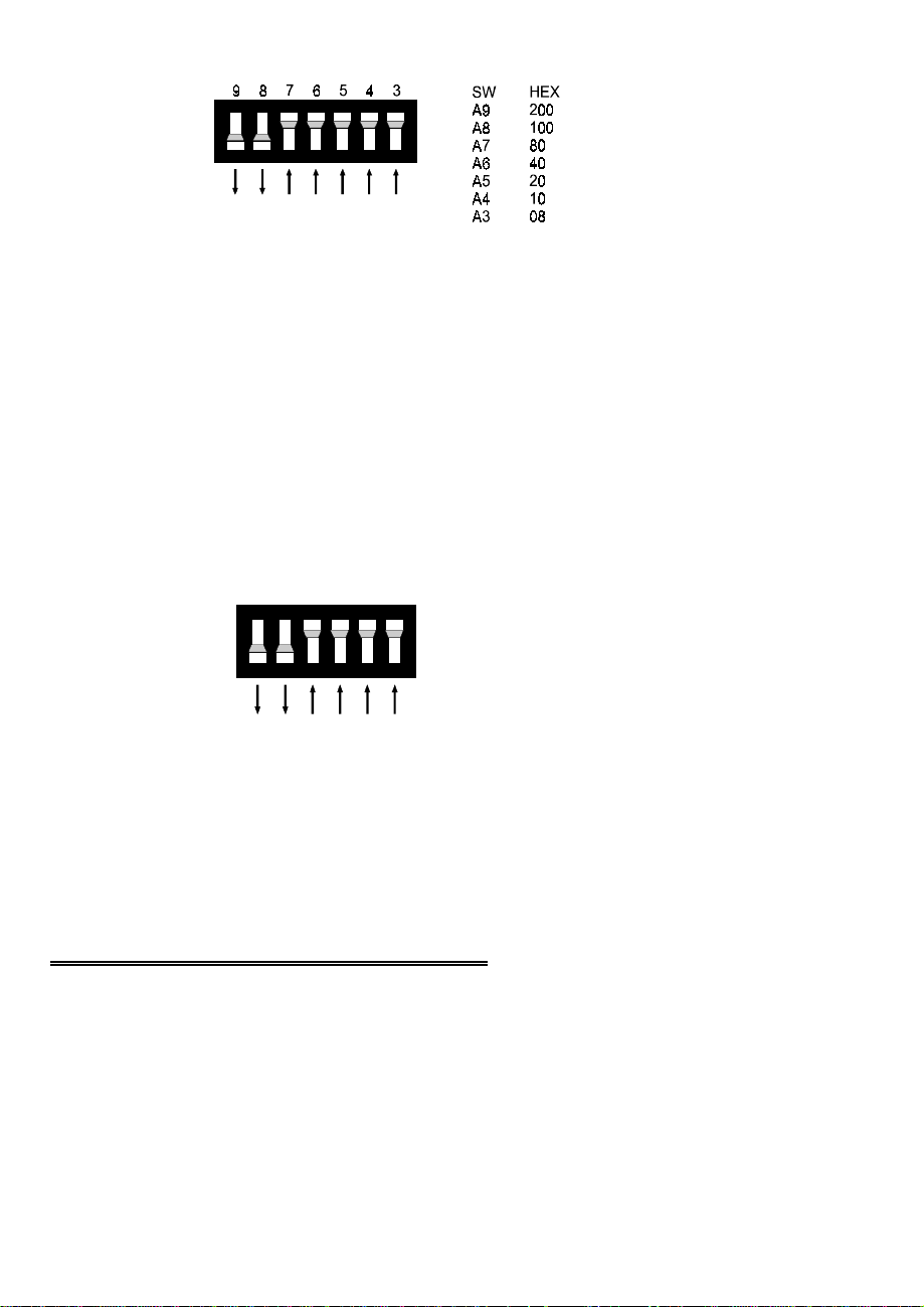
Figure 3-1. CIO-PDMA16 Base Address Switches (300h shown)
A complete address is constructed by calculating the hexadecimal number which
corresponds to all the address bits the CIO-PDMAx can respond to. The range of
base addresses are:
CIO-PDMA16 200h to 3F8h
CIO-PDMA32 200h to 3F0h
In the default configuration, shown in Figures 3-1 and 3-2, addresses 9 and 8 are
DOWN, and all others are UP. Address 9 = 200 hex (512 decimal) and address 8 =
100 hex (256 decimal). When added together they equal 300 hex (768 decimal).
9876
5
4
SW
A9
A8
A7
A6
A5
A4
HEX
200
100
80
40
20
10
Figure 3-2. CIO-PDMA32 Base Address Switches (300h shown)
NOTE: The CIO-PDMA32 has one fewer switch than the CIO-PDMA16.
NOTE
DISREGARD NUMBERS PRINTED ON THE SWITCH. REFER
ONLY TO WHITE NUMBERS PRINTED ON THE BOARD.
3.2 INTERRUPT & DMA LEVEL SELECT
The interrupt and DMA levels used by the CIO-PDMA boards are selected in
software. Refer to the documentation for the software package you are using to set
these parameters.
3
Page 8
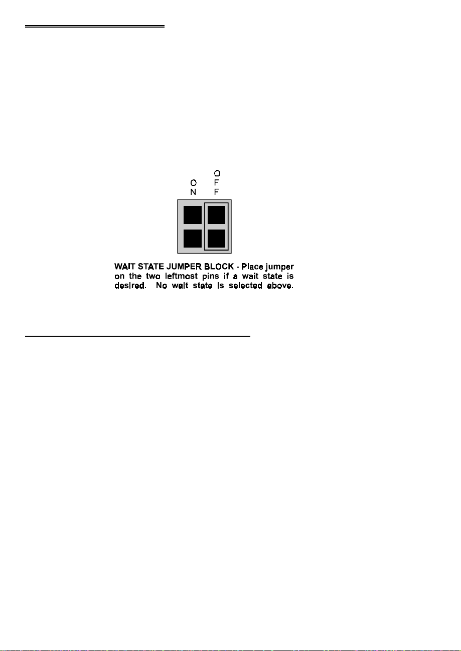
3.3 WAIT STATE JUMPER
The CIO-PDMA16 board has a wait state jumper (Figure 3-3) which can enable an
on-board wait-state generator. A wait state is an extra delay injected into the
processor's clock via the bus. This delay slows the processor slightly so that signals
from slow devices (chips) will be valid. The default position is Disabled. Only rarely,
and then only if processing fast signals, might the Enabled position be required.
NOTE: The wait state generator on the CIO-PDMA16 is only active when the board
is being accessed. In general, your PC will not be slowed down by using the wait
state.
Figure 3-3. Wait State Jumper Positions
3.4 INSTALLING THE CIO-PDMA BOARD
1. Shut the computer down, remove power, and open the case.
2. Locate an empty ISA expansion slot in your computer. The CIO-PDMA32 board
requires a 16-bit slot (with two connectors), while the CIO-PDMA16 can be
installed in either an 8-bit or a 16-bit slot.
3. Push the board firmly down into the expansion bus connector. If it is not seated
fully it may fail to work and could short circuit the PC bus power onto a PC bus
signal. This could damage the motherboard in your PC as well as the
CIO-PDMA board. Use the screw provided on your computer's backplate to
secure the board in it's location.
4. Replace the cover on the computer and turn it ON.
5. To verify proper installation, you should now run
function.
4
Insta
Cal and select the
Test
Page 9
4.0 CABLING TO THE CIO-PDMA##
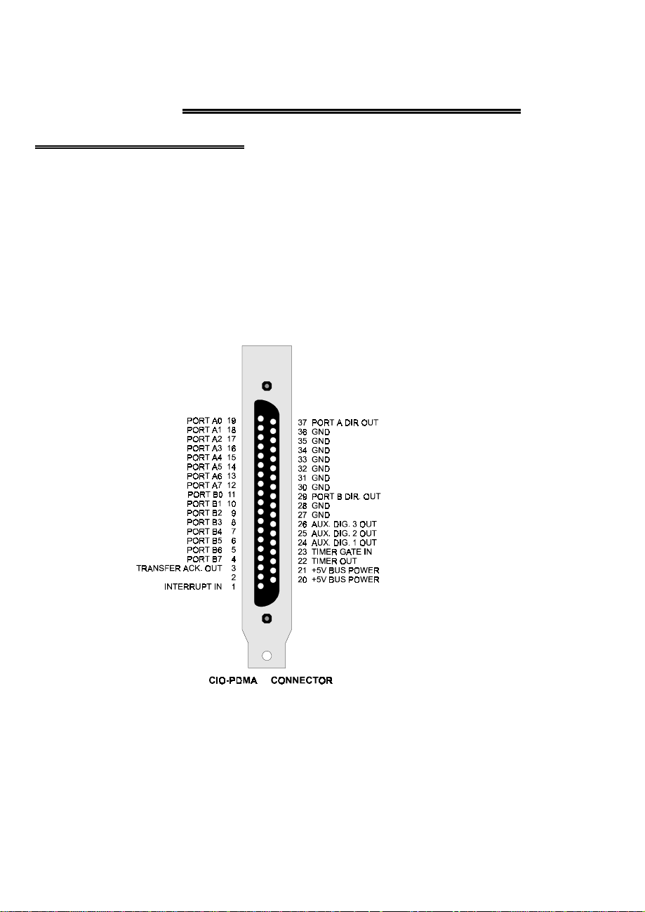
4.1 SIGNAL CONNECTIONS
The CIO-PDMA16 and CIO-PDMA32 connector is a 37-pin D-type connector
accessible from the rear of the PC through the expansion backplate.
The connector accepts female 37-pin D-type connectors, such as those on the
C37FF-2, 2-foot cable with connectors. If frequent changes to signal connections or
signal conditioning is required, please refer to the information on the
CIO-TERMINAL, CIO-SPADE50 and CIO-MINI37 screw terminal boards.
TRANSFER REQ IN
X
Figure 4-1. 37-Pin Signal Connector
5
Page 10

4.2 SIGNAL FUNCTIONAL DESCRIPTIONS
Port A input/output lines. A0 = LSBPORT A0 - A7
Port B input/output lines. B0 = LSBPORT B0 - B7
Output-only digital lines.AUX DIG 1- 3
Output only. 0 = input, 1 = outputPORT A DIR. OUT
Output only. 0 = input, 1 = outputPORT B DIR. OUT
TRANSFER REQ IN
TRANSFER ACK. OUT
TIMER GATE
INTERRUPT
Positive edge initiates a DMA transfer if DMA is
enabled and bit 3 of the DMA control register = 0.
This line goes low upon receipt of a TRANSFER
ACK. OUT then returns high after the DMA transfer
has completed. At that point, the transfer has taken
place and if it was an output, is valid to be read from
port(s) A (and B).
Output from 8254 counter 1. TIMER OUT
A low on this signal will hold the gates of 8254
counter 0 and counter 1 low, thereby inhibiting inputs
to the counters. This signal is pulled up by a 10K
resitor to +5V.
Positive or negative edge triggered input. Software
programmable.
4.3 DIGITAL OUTPUTS & INPUTS
All the digital inputs/outputs on the CIO-PDMA board are at TT L level. TTL is an
electronics industry term, short for Transistor-Transistor-Logic, which describes a
standard for digital signals which are either at 0V or 5V (nominal).
Under normal operating conditions, the voltages on Port A or P ort B pins range from
0 to 0.45 volts for the low (0) state to between 2.4 to 5.0 volts for the high (1) state.
At 0.45 volts, a port can safely sink 24 mA. At 2.4 volts, a port can source 2.6 mA.
These values are typical of TTL devices.
4.4 TERMINATING DIGITAL LINES
When transferring digital data at high rates over cables, the impedance of the cable
and both ends should be matched as closely as possible to avoid “ringing” or
reflections in the line. To accomplish this, it may be necessary to add resistors in
series with the data lines at the source of the signals.
6
Page 11

When the CIO-PDMA board is used as an output device to send data to another TTL
device over a standard ribbon cable, it may be necessary to add balancing resistors
(typically 220 Ohms) as close to the board as possible.
If the CIO-PDMA board is used as an input device, it may be necessary to add
resistors in series (220 Ohms typically) with the data lines, at the source of the signal.
Failure to observe these precautions may result in spurious signals being interpreted
by the receiver as valid data.
7
Page 12

5.0 REGISTER MAPS
5.1 CIO-PDMA16 REGISTER MAP
The CIO-PDMA16 and use eight consecutive I/O addresses in the PC's I/O address
space. The first address, or BASE ADDRESS, is determined by setting a bank of
switches on the board.
The first four addresses access the A & B data ports and DMA and interrupt control
registers of the CIO-PDMA16. The second four registers are directly mapped into the
8254 counter timer chip used for pacing CIO-PDMA16 transfers.
It is easy to read and write to a register. However, register manipulation is best left to
experienced programmers as most CIO-PDMA16 functions are done using Universal
Library.
In summary form, the registers and their function are listed in Table 5-1. Within each
register are eight bits which may constitute a byte of data or eight individual bit
set/read functions.
Table 5-1. Register Summary
WRITE FUNCTIONREAD FUNCTIONADDRESS
Port A OutputPort A InputBASE +0
Port B OutputPort B InputBASE +1
DMA Control, AUX1 & AUX2DMA read backBASE +2
Interrupt control, AUX3Interrupt read backBASE +3
Counter 0 dataCounter 0 dataBASE +4
Counter 1 dataCounter 1 dataBASE +5
Counter 2 dataCounter 2 dataBASE +6
Counter controlCounter statusBASE +7
5.1.1 DIGITAL I/O REGISTERS - PORTS A & B
Ports A & B may be written to or read from directly using I/O output or input
commands from any language that has such commands. In this way the
CIO-PDMA16 may be used as a simple digital I/O board.
As a DMA digital I/O board, ports A & B corresponds to the PC data bus. In DMA
word-transfers, port A data is transferred as the least significant byte and po rt B as the
most significant byte. DMA byte transfers use port A only. Port B cannot be used for
byte transfers under DMA.
8
Page 13

Ports A & B are set to input on power-up or hardware reset of the computer. The
direction of transfer, input/output, is controlled by one bit for each port in BASE + 2.
The inputs of the ports are one TTL load. The outputs can sink 24mA on output low. .
When the ports are configured for output and a read back is executed, the actual data
on the pins is read back. This may differ from what was written to the port if a chip is
faulty or a digital line is short circuited.
PORT A DATA
BASE ADDRESS + 0 300h, 768
10
01234567
A0A1A2A3A4A5A6A7
Pin 19Pin 18Pin 17Pin 16Pin 15Pin 14Pin 13Pin 12
PORT B DATA
BASE ADDRESS + 1 301h, 769
10
01234567
B0B1B2B3B4B5B6B7
Pin 11Pin 10Pin 9Pin 8Pin 7Pin 6Pin 5Pin 4
5.1.2 DMA CONTROL REGISTER
DMA control
BASE ADDRESS + 2 302h, 770
10
01234567
DMA
ENABLE
LEVEL
AUX1AUX2DMA
XFER
SOURCE
BYTE/
WORD
PORT B
DIR
PORT A
DIR
Pin 37Pin 29N/AN/APin 24Pin 25N/AN/A
FUNCTIONVALUEBIT NAME
Disabled0DMA ENABLE
Enabled1
Level 1 (channel 1)0DMA LEVEL
Level 3 (channel 3)1
Output only on pin 25XAUX2
Output only on pin 24XAUX1
External - from Transfer Req In, pin 2.0XFER SOURCE
Internal - 8254 timer1
Byte transfers0BYTE/WORD
Word transfers1
Input0PORT B DIR
Output1
Input0PORT A DIR
Output1
9
Page 14

The DMA control register is cleared on power-up or hardware reset. If you are
writing your own DMA routine, the DMA enable bit should be set before enabling the
8237 mask register.
DMA level selected by the DMA LEVEL bit is tri-stated when DMA ENABLE = 0.
Take care when writing to AUX1 and AUX2 that the current contents of the DMA
REGISTER are not disturbed.
5.1.3 INTERRUPT CONTROL REGISTER
Interrupt control
BASE ADDRESS + 3 302h, 770
10
01234567
SLOPEINT
ENABLE
AUX 3IR LEVIR LEVIR LEVINT
INT
SRC
SRC
N/AN/AN/APin 26N/AN/AN/AN/A
FUNCTIONVALUEBIT NAME
Disabled0INT ENABLE
Enabled1
Inactive000IR LEVEL
Inactive001
Level 2010
Level 3011
Level 4100
Level 5101
Level 6110
Level 7111
Output only on pin 26XAUX 3
External input00INT SRC (SOURCE)
8237 terminal count01
8254 timer10
8237 terminal count11
Positive edge0SLOPE
Negative edge1
The interrupt control register is cleared on power-up or hardware reset. If you are
writing your own interrupt routine, set the interrupt enable bit before enabling the
8259 mask register. The interrupt level selected by the IR LEVEL bit is tri-stated
when IR ENABLE = 0.
When writing to AUX1 and AUX2, take care not to disturb the current contents of the
INTERRUPT REGISTER.
10
Page 15

5.1.4 8254 COUNTER LOAD & READ REGISTERS
COUNTER 0
BASE ADDRESS + 4 304h, 772
10
01234567
D0D1D2D3D4D5D6D7
COUNTER 1
BASE ADDRESS + 5 305h, 773
10
01234567
D0D1D2D3D4D5D6D7
COUNTER 2
BASE ADDRESS + 6 306h, 774
10
01234567
D0D1D2D3D4D5D6D7
The data in the counter read register, and the action taken on the data in a counter load
register, is wholly dependent upon the control code written to the control register.
The counters have 16-bits, each with an 8-bit window, the read / load register. Data is
shifted in and out of the 16-bit counters through these 8-bit windows according to the
control byte.
You will need an 8254 data sheet if you want to program the 8254 directly in
assembly language or in BASIC or some other high level language.
5.1.5 COUNTER CONTROL REGISTER
BASE ADDRESS + 7 307h, 775
10
WRITE ONLY
SC1 to SC0 are the counter select bits. They are binary coded between 0 and 2.
SC1 SC0 Counter
0 0 0
0 1 1
1 0 2
11
01234567
BCDM0M1M2RL0RL1SC0SC1
Page 16

RL1 to RL0 are the read and load control bits:
RL1 RL0 OPERATION
0 0 Latch counter.
0 1 Read/load high byte.
1 0 Read/load low byte.
1 1 Read/load low then high byte (word transfer).
M2 to M0 are the counter control operation type bits:
M2 M1 M0 OPERATION TYPE
0 0 0 Change on terminal count.
0 0 1 Programmable one-shot.
0 1 0 Rate generator
0 1 1 Square wave generator
1 0 0 Software triggered strobe.
1 0 1 Hardware triggered strobe.
BCD = 0 then counter data is 16-bit binary. (65,535 max)
BCD = 1 then counter data is 4-decade Binary-Coded-Decimal. (9,999 max)
Figure 5-1. Pacer Clock Block Diagram
12
Page 17

5.2 CIO-PDMA32 REGISTER MAP
The PDMA-32 boards use 16 consecutive addresses starting at the Base Address in
the computers I/O space, as shown in the following table. The shaded areas highlight
the address space that the MetraByte PDMA-32 board uses. Note that MetraByte does
not use Addresses B to F hex.
TYPEFUNCTIONADDRESS
Read/writeA PortBase Address + 0
Read/writeB PortBase Address + 1
Read/writeDMA ControlBase Address + 2
Read/writeInterrupt ControlBase Address + 3
Read/writeCounter 0Base Address + 4
Read/writeCounter 1Base Address + 5
Read/writeCounter 2Base Address + 6
WriteCounter ControlBase Address + 7
ReadCounter Status
Read/writeDMA LevelBase Address + 8
Read/writeInterrupt LevelBase Address + 9
ReadInterrupt StatusBase Address + A
WriteFIFO ClearBase Address + B
Read/WriteREP ControlBase Address + C
WriteArmBase Address + D
Read/writeFIFOBase Address + E : F
5.2.1 PORTS A & B Base Address + 0 and Base Address + 1
These ports are the main digital I/O ports. Each port is 8-bits wide and can be used
individually or combined into one 16-bit port for programmed I/O, DMA I/O, or
rep-string I/O. Each port is associated with a data direction output (ADIR, BDIR).
Bits D0 and D1 of the DMA Control register select the data directions. On power-up,
ports are always reset to the Input mode.
A & B DirectionPort I/ODMA LevelBit D2
Byte for DMA or Rep-String
A & B IndependentByte for I/O0-3 (byte)0-Byte
A controls both portsWord for I/O0-3 (byte)1- Word
B IrrelevantByte (PA) for DMA or Rep-String
A controls both portsByte for I/O5-7 (word)0-Byte
B IrrelevantWord for DMA or Rep-String
A controls both portsWord for I/O5-7 (Word)1-Word
B IrrelevantWord for DMA or Rep-String
13
Page 18

Byte-wide DMA or Rep-String opera tions may be made only through Port A. If byte
mode is selected via the DMA Control Register (D2=0), then Port B is available and
independent of Port A for input or output using programmed I/O.
When word mode is selected via the DMA Control Register (D2=1), then the data
direction of Port B always follows the data direction of Port A.
Word-wide DMA or Rep-String operations are made through both Ports A and B
combined. In word mode, Port A provides the LSB and Port B the MSB of data. The
data direction of both ports has to be identical if a Word transfer DMA or Rep-string
(Level 5-7) is selected, and the B direction bit (D1 of the DMA Control Register), is
ignored both for DMA and Programmed I/O.
For normal Programmed (non-DMA) I/O, you have a choice of accessing the ports as
two separate byte-wide ports or configuring them as a single 16-bit word-wide port.
Notes:
1. Both ports are automatically set up in the input direction on power-up.
2. In Input mode, each line of Port A and B presents one TTL load to the driving
source. In Output mode, outputs of both ports will sink 24 mA and are TTL
compatible.
3. In Output Mode, data can be read back from either Port. This data corresponds to
the actual data on the output pins and may not correspond to d ata written if an
output line is shorted or faulty.
5.2.2 DMA Control Register
Base Address + 2
01234567
ENB
AUX1AUX20DMA
XFER
SRC
WORD
ADIRBDIRBYTE/
MSB LSB
DescriptionNameBit
0 = Disable, 1 = EnableDMAENB7
Auxiliary user outputAUX25
Auxiliary user outputAUX14
0 = EXT, 1 = internal C/TXFERSRC3
0 = Byte, 1 = WordBYTE/WORD2
0 = Input, 1 = OutputBDIR1
0 = Input, 1 = OutputADIR0
Notes:
1. The DMA Control Register is cleared on power-up (reset) of the computer, thus
disabling DMA and setting the ports as inputs.
14
Page 19

2. If word mode is selected for regular I/O (D2 = 1), then the B direction bit is
ignored. Both ports o perate as a single 16-bit port with the direction set by A
direction bit D0.
3. The XFERSRC bit is used in both REP and DMA modes to select the transfer
clock source.
5.2.3 Interrupt Control Register
The interrupt Control Register is an 8-bit read/write register.
Base Address + 3
01234567
INT
ENB
000
AUX3
INT
SRC1
SRC0
SLOPEINT
LSBMSB
DescriptionNameBit
0 = Disable, 1 = EnableINTENB7
Auxiliary user outputAUX33
INTSRC(1:0)2:1
00 = External Input
01 = 8237 Terminal Count
10 = Counter/Timer Terminal Count
11 = 8237 Terminal Count
0 = + Edge 1 = - EdgeSLOPE0
Notes:
1. The Interrupt Control Register is cleared on power-up, thus disabling interrupts.
2. When REP_ENB bit is set, the Interrupt Source automatically defaults to the
Counter/Timer Terminal Count.
5.2.4 Counter Load & Read Registers Base Address + 4, 5, 6, and 7
Counter 0
Base Address + 4
LSBMSB
Counter 1
Base Address + 5
LSBMSB
Counter 2
Base Address + 6 LSB
15
01234567
D0D1D2D3D4D5D6D7
01234567
D0D1D2D3D4D5D6D7
01234567
D0D1D2D3D4D5D6D7
Page 20

The data in the counter read register, and the action taken on the data in the counter
load register, is wholly dependent upon control code written to the control register.
The counters are 16 bits, each with an 8-bit window, the read/load register. Data are
shifted into and out of the 16-bit counters thro ugh these 8-bit windows according to
the control byte.
5.2.5 Counter Control Register
Base Address + 7
01234567
BCDM0M1M2RL0RL1SC0SC1
LSBMSB
SC1 and SC0 are the counter select bits. The are binary coded between 0 and 2.
SC1 SC2 Counter
0 0 0
0 1 1
1 0 2
RL1 and RL0 are the read and load control bits:
OperationRL0RL1
Latch counter.00
Read/load high byte.10
Read/load low byte.01
Read/load low then high byte (word transfer).11
M2 to M0 are the counter mode control bits:
Counter 0 and Counter 1 are hardware-fixed to operate in Rate Generator mode only.
Operation TypeM0M1M2
Rate Generator.010
Counter 2 can support the following two modes:
Operation TypeM0M1M2
Change on terminal count.000
Rate Generator.010
BCD = 0: The counters are hardware fixed to support 16-bit binary mode only.
16
Page 21

5.2.6 DMA Level Select Register
The level of DMA request generated by the board is determine via this register. This
register is also used to determine the port width during REP mode. This is a read/write
register. These bits a re cleared after reset. Note that the unused bits D7:D3 are still
user programmable.
Base Address + 8
01234567
xxxxx
L0L1L2
LSBMSB
L2, L1, L0 select the DMA level or REP Port size as follows:
000 = Level 0 (byte) 100 = Illegal
001 = Level 1 (byte) 101 = Level 5 (word)
010 = Level 2 (byte) 110 = Level 6 (word)
011 = Level 3 (byte) 111 = Level 7 (word)
x = don’t care
5.2.7 Interrupt Level Register
This is a read/write register used to program the desired interrupt level of the
PDMA-32 board . These bits ar e cleared after r eset. Note that the unuse d bits D7:D4
are user programmable. Interrupt priorities highest-to-lowest are 9, 10, 11, 12, 14, 15,
3, 4, 5, 6, and 7. There is no interrupt Level 2 on the PC/AT; it is redirected through
Interrupt Level 9.
Base Address + 9
01234567
xxxx
I0I1I2I3
MSB LSB
x = don’t care
5.2.8 Interrupt Status Register
This is a read only register. In DMA mode this register returns a single bit
corresponding to the state of the PDMA-32’s internal interrupt request. In REP mode
this register provides additional flag information regarding the status of the current
REP transfer. Reading the Interrupt Status Register will clear the pending interrupt
request and re-enable interrupts.
Base Address + Ah
01234567
IRQ
000
RUN
REP_DONEREP_FLGOVERRUNUNDER
MSB LSB
17
Page 22

DescriptionNameBit
1=Interrupt Pending, 0 = No InterruptIRQ7
UNDERRUN3
This bit is set when in REP_ENB mode and the FIFO
has been underrun. This flag indicates that the FIFO is
being unloaded too quickly.
OVERRUN2
This bit is set when in REP_ENB mode and the FIFO
has been overrun. This flag indicates that the FIFO is
being loaded too quickly
REP_FLG1
This bit is set when in REP_ENB mode and the FIFO is
half-full.
REP_DONE0
This bit is set when in REP_ENB mode, and the Sample
Counter has reached terminal count.
5.2.9 FIFO Clear Start Address Register
This is a write only register. A write to this register clears the FIFO address pointers to
zero. Data is don’t care. Prior to initiating a REP-STRING transfer the FIFO write and
read address pointers should always be cleared to a start address of 0.
Base Address + Bh
01234567
XXXXXXXX
MSB LSB
5.2.10 REP String Control Register
This is a read/write register. These bits are in the inactive reset state after power-up.
Base Address + Ch
01234567
REP_
MODE
REP_
ENB
REP_
CONT
HALF_
FF_CNT
BUFF
ERR_ENBDBL_
xx
MSB LSB
18
Page 23

DescriptionNameBit
REP_MODE7
REP_ENB6
REP_CONT5
HALF_FF_CNT4
DBL_BUFF3
ERR_ENB2
When this bit is set REP mode is enabled. When this bit is
cleared REP mode is disabled and interrupt status
corresponding to the REP function is also inactive.
When this bit is set REP-STRING sequence is initiated. This
bit is automatically cleared when the current RE P-STRING
transfer has completed (the sample counter reaches terminal
count).
When this bit is set, the REP-STRING sequence operates in
continuous mode. In this mode the ARM register is enabled
and is used to trigger the termination of the current REP
transfer.
When this bit is cleared, the sample counter (8254 Counter
2) is used to count the total number of samples to be
transferred (the sample counter decrements at the pacer
sample rate). When this bit is set and in REP-STRING mode,
the sample counter is used to count the total number of halffull FIFO transfers to be transferred (the sample counter
decrements at the half-full rate)
When this bit is set, port A and B outputs are doublebuffered so that the outputs are updated in sync with the
pacer clock. When th is bit is cleared, port A and B outputs
are updated immediately following the write to the
corresponding port registers.
When this bit is set, the OVERRUN and UNDERRUN error
flags are enabled. The error flags should be enabled when a
REP transfer size of greater than one FIFO in depth is
required (512 bytes).
CommentsHALF_FF_CNT_REP_CONT
00
00
1
0
11
In REP mode this configuration can be used when
the transfer size is less than 65536 bytes. The 16-bit
counter is used to count the actual number of
samples.
In REP mode this configuration can be used when
the transfer size is less than 16.7 Mbytes and an
integer multiple of 256 bytes. The 16-bit counter is
used to count the number of half-full FIFO transfers.
In REP mode the 16-bit counter can be used as a
residual counter. In this mode the CIO-PDMA32
can support unlimited transfer sizes. Once armed,
the residual counter is used to count the actual
number of samples.
In REP mode the 16-bit counter can be used as a
residual counter. In this mode the board can support
unlimited transfer sizes. Once armed, the residual
counter is used to count the actual number of
half-full FIFO transfers.
19
Page 24

5.2.11 REP mode ARM register
This is a write-only register. In continuous REP mode, a write to this register arms the
sample counter. Once armed, the sample counter does not start decrementing until a
half- full FIFO boundary has been reached. Data is don’t-care.
Base Address + Dh
01234567
XXXXXXXX
LSB
5.2.12 FIFO Register
The FIFO is accessed via this 16-bit read/write register at BASE + Eh.
The data format is:
Base Address + Eh
89101112131415
B0B1B2B3B4B5B6B7
MSB
LSB
01234567
A0A1A2A3A4A5A6A7
20
Page 25

6.0 SPECIFICATIONS
Typical for 25°C unless otherwise specified.
Power Consumption
+5VDC
CIO-PDMA16 850 mA typical, 1.0 A max
CIO-PDMA32 900 mA typical, 1.1 A max
Digital Input / Output
Digital Type Auxiliary
Configuration Output
Number of channels 3
CIO-PDMA16
Output High 2.7 volts min @ −0.4 mA
Output Low 0.5 volts max @ 8 mA
Input High 2.0 volts min, 7 volts absolute max.
Input Low 0.8 volts max, −0.5 volts absolute min
CIO-PDMA32
Output High 2.4 volts min @ −2.6 mA
Output Low 0.5 volts max @ 24 mA
Input High 2.0 volts min, 7 volts absolute max
Input Low 0.8 volts max, −0.5 volts absolute min
74LS273
74LS125
Digital Type Ports A & B
CIO-PDMA16
Output 74LS374
Input 74LS244
CIO-PDMA32 74LS245
Number of channels 16 I/O
Output High 2.4 volts min @ −2.6 mA
Output Low 0.5 volts max @ 24 mA
Input High 2.0 volts min, 7 volts absolute max
Input Low 0.8 volts max, −0.5 volts absolute min
Power-up / Reset State
Digital Pacing
Input mode (high impedance)
Programmable: internal counter, external
source (Transfer Req In) or software polled
21
Page 26

Data Transfer
CIO-PDMA16 Interrupt, DMA or software polled
CIO-PDMA32 From 512 sample FIFO via REPINSW,
interrupt, DMA or software polled
DMA
CIO-PDMA16 Channel 1 or 3, software selectable
CIO-PDMA32 Channel 5, 6, or 7,software selectable
Throughput
CIO-PDMA16 250K Bytes, 125K Words / sec synchronous
CIO-PDMA32 (DMA) 400K Bytes, 200K Words / sec synchronous
CIO-PDMA32 (REPIN/OUTS) 1500K Bytes, 750K Words / sec
synchronous
Interrupts
CIO-PDMA16 Levels 2 - 7, software-selectable
CIO-PDMA32 Levels 2 - 15, software-selectable
Interrupt enable Programmable
Interrupt sources External (Int In, positive or negative edge
software-selectable), DMA terminal count,
Counter / Timer terminal count,
software-selectable
Counter section
Counter type
CIO-PDMA16 82C54
CIO-PDMA32 82C54 emulator
Configuration 3 down-counters per 82C54, 16 bits each
Counter 0 - Internal pacer, lower divider (mode 2 only
for CIO-PDMA32)
Source: 10 MHz oscillator
Gate: Wired to counter 1 gate, pulled high
through 10k resistor. Available at user
connector (Timer Gate In)
Output: Wired to counter 1 and counter 2 clock
inputs
Counter 1 - Internal pacer, upper divider (mode 2 only
for CIO-PDMA32)
Source: Counter 0 output
Gate: Wired to counter 0 gate, pulled high
through 10k resistor. Available at user
connector (Timer Gate In)
Output: Wired through inverter to user connector
(Timer Out). Program-selectable as DMA
Request source (internal pacer)
22
Page 27

Counter 2 - CIO-PDMA16 (user counter 3)
Source: Counter 0 output.
Gate: Pulled high through 10k resistor
Output: Not connected
Counter 2 - CIO-PDMA32 Used internally for REPINS
/ REPOUTS modes (configured as mode 2
8254 emulator)
Source: Internal use
Gate: Internal use
Output: Internal use
Clock input frequency 10 MHz max
High pulse width (clock input) 30 ns min
Low pulse width (clock input) 50 ns min
Gate width high 50 ns min
Gate width low 50 ns min
Input low voltage 0.8V max
Input high voltage 2.0V min
Output low voltage 0.4V max
Output high voltage 3.0V min
Crystal oscillator
Frequency 10 MHz
Frequency accuracy 100 ppm
Environmental
Operating temperature range 0 to 60°C
Storage temperature range −40 to 100°C
Humidity 0 to 90% non-condensing
23
Page 28

For your notes.
24
Page 29

For your notes.
25
Page 30

For your notes.
26
Page 31

EC Declaration of Conformity
We, Measurement Computing Corporation, declare under sole responsibility that the
product:
CIO-PDMA16 &
CIO-PDMA32
to which this declaration relates, meets the essential requirements, is in conformity
with, and CE marking has been applied according to the relevant EC Directives listed
below using the relevant section of the following EC standards and other normative
documents:
EU EMC Directive 89/336/EEC
compatibility.
EU 55022 Class B
characteristics of information technology equipment.
EN 50082-1
IEC 801-2
and control equipment.
IEC 801-3
measurements and control equipment.
IEC 801-4
equipment.
: Electrostatic discharge requirements for industrial process measurement
: Radiated electromagnetic field requirements for industrial process
: Electrically fast transients for industrial process measurement and control
: Limits and methods of measurements of radio interference
: EC generic immunity requirements.
High speed digital I/O board
Ultra High speed digital I/O board
DescriptionPart Number
: Essential requirements relating to electromagnetic
Carl Haapaoja, Director of Quality Assurance
Page 32

Measurement Computing Corporation
16 Commerce Boulevard,
Middleboro, MA 02346
(508) 946-5100
Fax: (508) 956-9500
E-mail: info@measurementcomputing.com
www. measurementcomputing.com
 Loading...