

Page 1
Page 2

CIO-DDA06
Analog Output Board
User’s Guide
Document Revision 7, December, 2006
© Copyright 2006, Measurement Computing Corporation
Page 3

Your new Measurement Computing product comes with a fantastic extra —
Management committed to your satisfaction!
Refer to www.mccdaq.com/execteam.html for the names, titles, and contact information of each key executive at Measurement
Computing.
Thank you for choosing a Measurement Computing product—and congratulations! You own the finest, and you can now enjoy
the protection of the most comprehensive warranties and unmatched phone tech support. It’s the embodiment of our mission:
To provide PC-based data acquisition hardware and software that will save time and save money.
Simple installations minimize the time between setting up your system and actually making measurements. We offer quick and
simple access to outstanding live FREE technical support to help integrate MCC products into a DAQ system.
Lifetime warranty: Every hardware product manufactured by Measurement Computing Corporation is warranted against
defects in materials or workmanship for the life of the product. Products found defective are repaired or replaced promptly.
Lifetime Harsh Environment Warranty®: We will replace any product manufactured by Measurement Computing
Corporation that is damaged (even due to misuse) for only 50% of the current list price. I/O boards face some tough operating
conditions, some more severe than the boards are designed to withstand. When a board becomes damaged, just return the unit
with an order for its replacement at only 50% of the current list price. We don’t need to profit from your misfortune. By the way,
we honor this warranty for any manufacturer’s board that we have a replacement for.
30 Day Money Back Guarantee: You may return any Measurement Computing Corporation product within 30 days of
purchase for a full refund of the price paid for the product being returned. If you are not satisfied, or chose the wrong product by
mistake, you do not have to keep it. Please call for an RMA number first. No credits or returns accepted without a copy of the
original invoice. Some software products are subject to a repackaging fee.
These warranties are in lieu of all other warranties, expressed or implied, including any implied warranty of merchantability or
fitness for a particular application. The remedies provided herein are the buyer’s sole and exclusive remedies. Neither
Measurement Computing Corporation, nor its employees shall be liable for any direct or indirect, special, incidental or
consequential damage arising from the use of its products, even if Measurement Computing Corporation has been notified in
advance of the possibility of such damages.
HM CIO-DDA06.doc
3
Page 4

Trademark and Copyright Information
TracerDAQ, Universal Library, Harsh Environment Warranty, Measurement Computing Corporation, and the Measurement
Computing logo are either trademarks or registered trademarks of Measurement Computing Corporation.
Windows, Microsoft, and Visual Studio are either trademarks or registered trademarks of Microsoft Corporation
LabVIEW is a trademark of National Instruments.
CompactFlash is a registered trademark of SanDisk Corporation.
XBee and XBee-PRO are trademarks of MaxStream, Inc.
All other trademarks are the property of their respective owners.
Information furnished by Measurement Computing Corporation is believed to be accurate and reliable. However, no
responsibility is assumed by Measurement Computing Corporation neither for its use; nor for any infringements of patents or
other rights of third parties, which may result from its use. No license is granted by implication or otherwise under any patent or
copyrights of Measurement Computing Corporation.
All rights reserved. No part of this publication may be reproduced, stored in a retrieval system, or transmitted, in any form by
any means, electronic, mechanical, by photocopying, recording, or otherwise without the prior written permission of
Measurement Computing Corporation.
Notice
Measurement Computing Corporation does not authorize any Measurement Computing Corporation product for use
in life support systems and/or devices without prior written consent from Measurement Computing Corporation.
Life support devices/systems are devices or systems which, a) are intended for surgical implantation into the body,
or b) support or sustain life and whose failure to perform can be reasonably expected to result in injury.
Measurement Computing Corporation products are not designed with the components required, and are not subject
to the testing required to ensure a level of reliability suitable for the treatment and diagnosis of people.
4
Page 5

Table of Contents
Preface
About this User's Guide .......................................................................................................................6
What you will learn from this user's guide.........................................................................................................6
Conventions in this user's guide .........................................................................................................................6
Where to find more information.........................................................................................................................6
Chapter 1
Introducing the CIO-DDA06 .................................................................................................................7
Overview: CIO-DDA06 features........................................................................................................................7
Software features................................................................................................................................................7
Chapter 2
Installing the CIO-DDA06 .....................................................................................................................8
What comes with your CIO-DDA06 shipment?.................................................................................................8
Hardware .......................................................................................................................................................................... 8
Additional documentation................................................................................................................................................. 8
Optional components..........................................................................................................................................8
Unpacking the CIO-DDA06...............................................................................................................................9
Installing the software ........................................................................................................................................9
Configuring the CIO-DDA06.............................................................................................................................9
Base address switch .......................................................................................................................................................... 9
Wait state jumper.............................................................................................................................................................10
Individual / simultaneous transfer jumper........................................................................................................................10
Power up and reset jumper...............................................................................................................................................11
Analog output range switch .............................................................................................................................................12
Installing the CIO-DDA06 ...............................................................................................................................12
Connecting the board for I/O operations ..........................................................................................................13
Connectors, cables – main I/O connector ........................................................................................................................13
Pinout – main I/O connector............................................................................................................................................13
Cabling.............................................................................................................................................................................14
Field wiring, signal termination, and conditioning ..........................................................................................................14
Chapter 3
Programming and Developing Applications ....................................................................................15
Programming languages ...................................................................................................................................15
Packaged applications programs ......................................................................................................................15
Register-level programming.............................................................................................................................15
Chapter 4
Functional Details ...............................................................................................................................16
CIO-DDA06 block diagram .............................................................................................................................16
Signal connections............................................................................................................................................16
Chapter 5
Specifications......................................................................................................................................17
Analog output ...................................................................................................................................................17
Digital input / output ........................................................................................................................................18
Power consumption ..........................................................................................................................................18
Environmental ..................................................................................................................................................18
Main connector and pin out..............................................................................................................................18
5
Page 6

Preface
About this User's Guide
What you will learn from this user's guide
This user's guide explains how to install, configure, and use the CIO-DDA06 board so that you get the most out
of its analog output features. This user's guide also refers you to related documents available on our web site,
and to technical support resources.
Conventions in this user's guide
The following conventions are used in this manual to convey special information:
For more information on …
Text presented in a box signifies additional information and helpful hints related to the subject matter you are
reading.
Caution! Shaded caution statements present information to help you avoid injuring yourself and others,
damaging your hardware, or losing your data.
<#:#> Angle brackets that enclose numbers separated by a colon signify a range of numbers, such as those assigned
to registers, bit settings, etc.
bold text Bold text is used for the names of objects on the screen, such as buttons, text boxes, and check boxes. For
example:
1. Insert the disk or CD and click the OK button.
italic text Italic text is used for the names of manuals and help topic titles, and to emphasize a word or phrase. For
example:
The InstaCal installation procedure is explained in the Quick Start Guide.
Never touch the exposed pins or circuit connections on the board.
Where to find more information
The following electronic documents provide information relevant to the operation of the CIO-DDA06.
MCC's Specifications: CIO-DDA06 (the PDF version of the Specifications chapter in this guide) is
available on our web site at www.mccdaq.com/pdfs/CIO-DDA06.pdf
MCC's Quick Start Guide is available on our web site at
www.mccdaq.com/PDFmanuals/DAQ-Software-Quick-Start.pdf
MCC's Guide to Signal Connections is available on our web site at
www.mccdaq.com/signals/signals.pdf
MCC's Universal Library User's Guide is available on our web site at
www.mccdaq.com/PDFmanuals/sm-ul-user-guide.pdf
MCC's Universal Library Function Reference is available on our web site at
www.mccdaq.com/PDFmanuals/sm-ul-functions.pdf
MCC's Universal Library for LabVIEW
www.mccdaq.com/PDFmanuals/SM-UL-LabVIEW.pdf
.
.
™
User’s Guide is available on our web site at
.
.
.
.
CIO-DDA06 User's Guide (this document) is also available on our web site at
www.mccdaq.com/PDFmanuals/CIO-DDA06.pdf
.
6
Page 7

Chapter 1
Introducing the CIO-DDA06
Overview: CIO-DDA06 features
The CIO-DDA06 has six channels of 12-bit analog output and 24 lines of digital I/O. Analog outputs are dualDAC AD7273s (two analog outputs per chip), with each output buffered by an OP07. Digital I/O is performed
with one 82C55 chip. The CIO-DDA06 is 100% compatible with MetraByte's DDA-06.
Analog output ranges are switch-selectable for a Bipolar or Unipolar range. Bipolar ranges are ±10 V, ±5 V,
±2.5 V, and ±1.67 V. Unipolar ranges are 0 to 10 V, 0 to 5 V, 0 to 2.5 V, and 0 to 1.67 V.
Analog outputs are grouped in pairs (0/1, 2/3, and 4/5). Each analog output pair is jumper-selectable for either
individual or simultaneous transfer in groups of two, four, or all six.
When a DAC pair is set for simultaneous update, the CIO-DDA06 may be set to hold new values until all
channels are loaded, then update any two, four, or all six channels simultaneously.
The CIO-DDA06 digital I/O lines are a direct interface to an 82C55. The 82C55 is a CMOS chip with TTL
level inputs and outputs. The 8255 can source or sink about 2.5 mA. This is adequate to switch other TTL or
similar inputs, but is inadequate to drive relays, LEDs or solid state relays. The digital I/O is controlled by
programming the 8255's mode register. There are three possible modes. The simplest and most commonly used
mode is mode 0 — simple input and output.
The power up and reset state is jumper-selectable (hardware revision 3 and later). You can also enable a wait
state generator with an on-board jumper.
Software features
For information on the features of InstaCal and the other software included with your CIO-DDA06, refer to the
Quick Start Guide that shipped with your device. The Quick Start Guide is also available in PDF at
www.mccdaq.com/PDFmanuals/DAQ-Software-Quick-Start.pdf
Check www.mccdaq.com/download.htm
for the latest software version.
.
7
Page 8

Installing the CIO-DDA06
What comes with your CIO-DDA06 shipment?
The following items are shipped with the CIO-DDA06.
Hardware
CIO-DDA06
Chapter 2
Additional documentation
In addition to this hardware user's guide, you should also receive the Quick Start Guide (available in PDF at
www.mccdaq.com/PDFmanuals/DAQ-Software-Quick-Start.pdf
the software you received with your CIO-DDA06 and information regarding installation of that software.
Please read this booklet completely before installing any software or hardware.
). This booklet supplies a brief description of
Optional components
Cables
C37FF-x
Signal termination and conditioning accessories
MCC provides signal conditioning and termination products for use with the CIO-DDA06. Refer to Field
wiring, signal termination, and conditioning on page 14 for a complete list of compatible accessory
products.
C37FFS-x
8
Page 9

CIO-DDA06 User's Guide Installing the CIO-DDA06
Unpacking the CIO-DDA06
As with any electronic device, you should take care while handling to avoid damage from static
electricity. Before removing the CIO-DDA06 from its packaging, ground yourself using a wrist strap or by
simply touching the computer chassis or other grounded object to eliminate any stored static charge.
If any components are missing or damaged, notify Measurement Computing Corporation immediately by
phone, fax, or e-mail:
Phone: 508-946-5100 and follow the instructions for reaching Tech Support.
Fax: 508-946-9500 to the attention of Tech Support
Email: techsupport@mccdaq.com
Installing the software
Refer to the Quick Start Guide for instructions on installing the software on the Measurement Computing Data
Acquisition Software CD. This booklet is available in PDF at www.mccdaq.com/PDFmanuals/DAQ-Software-
Quick-Start.pdf.
Configuring the CIO-DDA06
The CIO-DDA06 has one base address switch, one bank of gain switches for each analog output channel, a
simultaneous update jumper for each DAC pair, a "power-up state" selection jumper, and one wait state jumper.
The InstaCal calibration and test program will show you how to set the switches. Run InstaCal before you open
your computer and install the board.
The CIO-DDA06 is shipped with the factory-default settings listed in the table below.
Factory-configured default settings
Board label Switch/jumper description Default setting
ADDRESS
WAIT STATE
XFER
UPDATE ##
GAIN #
PWR UP
DIP switch for setting the base address 300h (768 decimal)
Jumper to enable a wait state generator OFF position (disabled)
Jumpers to select simultaneous or single channel
update for each DAC channel pair
DIP switches to set the output range for each
analog output channel
Jumper to select the power up and reset state STD position — standard mode (undefined
UPDATE position (single channel update)
±5V
output values at power up)
Before installing the CIO-DDA06 in the computer, verify that the board is configured with the settings that you
want. Review the following information to change the default configuration of a jumper or switch on the CIODDA06 board.
Base address switch
Set the base address with the dip switch labeled ADDRESS located on the board.
The easiest way to set the base address switch is to let InstaCal show you the correct settings. However, if are
already familiar with setting ISA base addresses, you may use the base address switch description below to
guide your base address selection.
Unless there is already another board in your system using address 300 hex (768 decimal), leave the switches as
they are set at the factory. shows the base address switch set to its factory-default base address of
Figure 1
300 hex.
9
Page 10

CIO-DDA06 User's Guide Installing the CIO-DDA06
A
Address 9
DDRESS
5
9876
Figure 1. Base address switch
= 200 hex (512 decimal), and address 8 = 100 hex (256 decimal). When added together they equal
gure 1In the default configuration shown in Fi , addresses 9 and 8 are DOWN, and all others are UP.
4
SW
A9
A8
A7
A6
A5
A4
HEX
200
100
80
40
20
10
300 hex (768 decimal).
Disregard the numbers printed on the switch
When setting the base address, refer to the numbers printed in white on the printed circuit board.
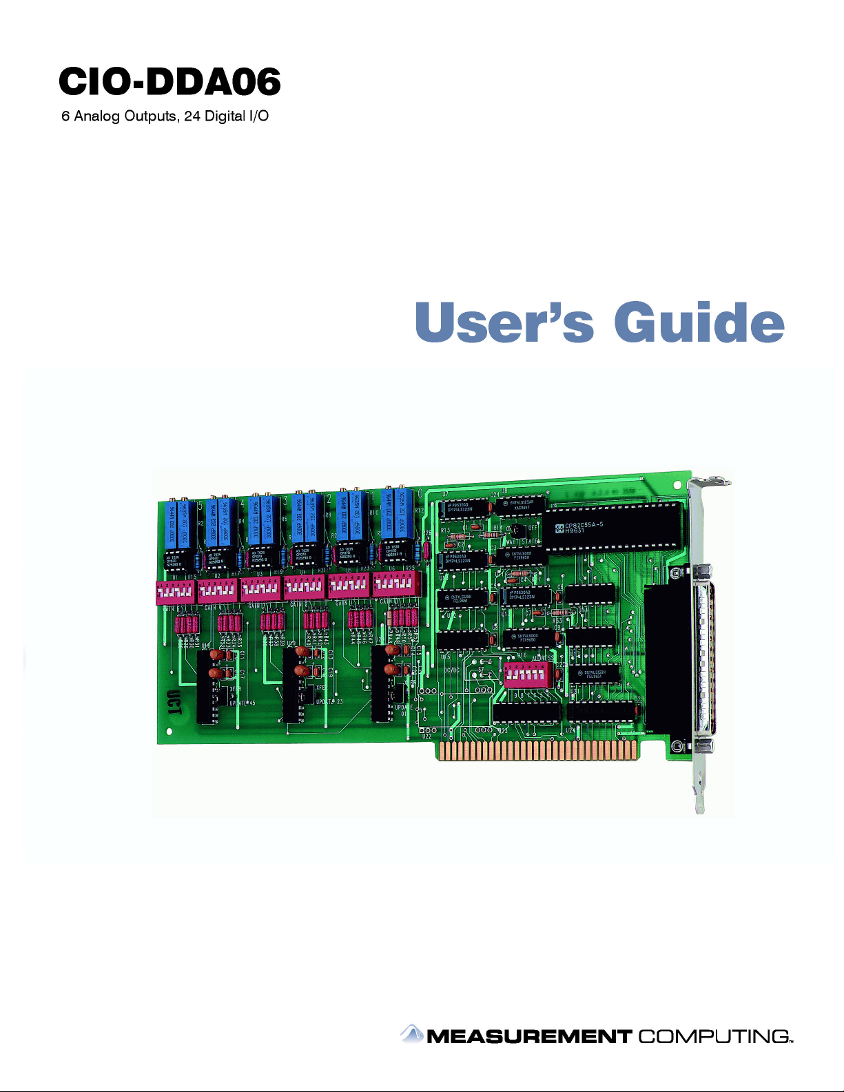
Wait state jumper
The CIO-DDA06 board has a wait state jumper which you can set to enable an on-board wait state generator. A
wait state is an extra delay injected into the processor's clock via the bus. This delay slows down the processor
when the processor addresses the CIO-DDA06 board so that signals from slow devices (chips) will be valid.
This jumper is shown in configured for OFF (wait state is disabled). Figure 2
ON
Figure 2. Wait State jumper
OFF
The wait state generator on the CIO-DDA06 is only active when the CIO-DDA06 is being accessed. Your PC
will not be slowed down in general by using the wait state.
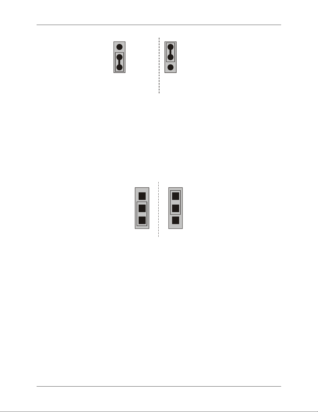
Individual / simultaneous transfer jumper
The analog outputs can be jumpered so that new output data is held until several DACs have been loaded with
new digital data. Then, as a group, the data for each DAC is simultaneously transferred and the DAC voltage
outputs are updated when any of the addresses BASE + 0 to BASE + B are read.
The analog output chips on the CIO-DDA06 are dual DACs (two analog outputs per chip). Each DAC channel
pair has an associated jumper that sets both DACs on a single chip to be either simultaneously transferred on a
read, or individually updated when the control register is written.
Figure 3 shows the jumper block configured for each update mode. Two numbers are listed on the board next to
each simultaneous transfer jumper (45, 23, and 01 from left to right). The numbers indicate which channel pair
is configured by the jumper (channels 0 and 1, 2 and 3, 4 and 5).
10
Page 11
CIO-DDA06 User's Guide Installing the CIO-DDA06
d
XFER
UPDATE # #
Individual updates
per DAC
(two channels)
Simultaneous updates
XFER
UPDATE # #
from all DACS
jumpered to XFER
Figure 3. Individual / simultaneous update jumper
When the jumpers are in the XFER position, new output data is held until one or more DACs have been
loaded with new digital data. The new data transfers to the voltage outputs as a group. The simultaneous
transfers occur when any of the CIO-DDA06 addresses are read (and the jumpers are in the
XFER
position).
When the jumpers are in the
UPDATE ## position, the DAC channel pair is individually updated when the
control register is written.
Power up and reset jumper
The power up and reset jumper (hardware revision 3 and later) controls the state of the DAC outputs when the
CIO-DDA06 board is powered up or reset. This jumper is shown in Fi . gure 4
STD
STD
ZERO
zero volts
power up
ZERO
Undefine
power up
Figure 4. Power up and reset jumper
When set for ZERO, all DACs are cleared to 0 volts, ±32 mV on power up and reset. In addition, all DACs
are set to simultaneous update mode until first read.
When set for
STD, the analog output values are undefined on power up and reset.
11
Page 12

CIO-DDA06 User's Guide Installing the CIO-DDA06
Analog output range switch
The analog output voltage range of each channel can be set with a set of six-position DIP switches. The switch
blocks are located on the board below the calibration potentiometers. The switch blocks are labeled
GAIN 5, and individual switches are labeled 1 through 6. Set the switches for each individual channel as shown
in . Figure 5
GAIN #
GAIN 0 to
Range
10
5.0
2.5
1.67
1.67
UP
UP
UP
UP
DN
DN
DN
DN
±
±
±
±
0-10
0-5
0-2.5
0-
Figure 5. Analog output range switch — one per DAC — configured for ±5 V
2
1
DN
DN
DN
DN
UP
UP
UP
UP
4
DN
UP
DN
DN
DN
UP
DN
DN
5
DN
DN
UP
DN
DN
DN
UP
DN
6
DN
DN
DN
UP
DN
DN
DN
UP
(Shown)
To set a channel to a particular range, read the switch positions as UP or DN (down) from left to right in the
row beside the range you want to set. The switch shown in Fi is configured for ±5V range (switch
gure 5
settings UP>DN>DN>UP>DN>DN).
Installing the CIO-DDA06
After you configure the board's switches and jumpers, you can install the CIO-DDA06 into your computer. To
install your board, follow the steps below.
Install the MCC DAQ software before you install your board
The driver needed to run your board is installed with the MCC DAQ software. Therefore, you need to install
the MCC DAQ software before you install your board. Refer to the Quick Start Guide for instructions on
installing the software.
1.
Turn your computer off, open it up, and insert your board into an available ISA slot.
2.
Close your computer and turn it on.
3.
To test your installation and configure your board, run the InstaCal utility you installed in the previous
section. Refer to the Quick Start Guide that came with your board www.mccdaq.com/PDFmanuals/DAQ-
Software-Quick-Start.pdf for information on how to initially set up and load InstaCal.
12
Page 13

CIO-DDA06 User's Guide Installing the CIO-DDA06
Connecting the board for I/O operations
Connectors, cables – main I/O connector
The table below lists the board connector, applicable cables, and compatible accessory products.
Board connector, cables, and accessory equipment
Connector type 37-pin male "D" connector
Compatible cables C37FF-x
C37FFS-x
DFCON-37 (D-connector, D-shell, and termination pins to construct your own cable)
Compatible accessory products
with the C37FF-x cable or
C37FFS-x cable
Information on signal connections
General information regarding signal connection and configuration is available in the Guide to Signal
Connections (available at www.mccdaq.com/signals/signals.pdf).
CIO-MINI37
CIO-TERMINAL
SCB-37
SSR-RACK24, ERB24, RACK08, ERB08
ENC-MINI37
Pinout – main I/O connector
The CIO-DDA06 I/O connector is a standard 37-pin male connector that is accessible through the PC/AT
expansion bracket.
LLGND 19
D/A OUT 0 18
LLGND 17
D/A OUT 1
LLGND 15
D/A OUT 2
LLGND 13
D/A OUT 3
FIRSTPORT B Bit 0 10
FIRSTPORT B Bit 1
FIRSTPORT B Bit 2
FIRSTPORT B Bit 3
FIRSTPORT B Bit 4
FIRSTPORT B Bit 5
FIRSTPORT B Bit 6
FIRSTPORT B Bit 7
DGND 11
D/A OUT 4
D/A OUT 5
16
14
12
9
8
7
6
5
4
3
2
1
37
FIRSTPORT A Bit 0
36
FIRSTPORT A Bit 1
35
FIRSTPORT A Bit 2
34
FIRSTPORT A Bit 3
33
FIRSTPORT A Bit 4
32
FIRSTPORT A Bit 5
31
FIRSTPORT A Bit 6
30
FIRSTPORT A Bit 7
29
FIRSTPORT C Bit 0
28
FIRSTPORT C Bit 1
27
FIRSTPORT C Bit 2
26
FIRSTPORT C Bit 3
25
FIRSTPORT C Bit 4
24
FIRSTPORT C Bit 5
23
FIRSTPORT C Bit 6
22
FIRSTPORT C Bit 7
21 LLGND
20 LLGND
Figure 6. I/O connector pin-out
The analog outputs are two-wire hook-ups. Always use low-level ground (LLGND) as the ground reference for
all analog hook-ups.
All the digital outputs inputs are TTL level. Before connecting external devices, review the specifications in
this manual to avoid damage to the CIO-DDA06.
13
Page 14

CIO-DDA06 User's Guide Installing the CIO-DDA06
Cabling
The red stripe
1
20
37
19
identifies pin # 1
Figure 7. C37FF-x cable
1
20
37
19
Figure 8. C37FFS-x cable
Field wiring, signal termination, and conditioning
1
19
20
37
1
20
37
19
You can use the following cabling, screw termination, and signal conditioning products with the CIO-DDA06.
DFCON37 – Connector kit that includes a 37-pin female D-connector, D-shell, 37 crimp pins, and cable
termination kit to construct your own cable. Details on this product are available on our web site at
www.mccdaq.com/cbicatalog/cbiproduct.asp?dept_id=103&pf_id=304
.
CIO-MINI37 – 37-pin screw terminal board. Details on this product are available at
www.mccdaq.com/cbicatalog/cbiproduct.asp?dept_id=102&pf_id=255
.
CIO-TERMINAL – 37-pin screw terminal board with on-board prototyping area. Details on this product
are available on our web site at www.mccdaq.com/cbicatalog/cbiproduct.asp?dept_id=102&pf_id=282
.
SCB-37 – 37-conductor, shielded signal connection/screw terminal box. Details on this product are
available on our web site at www.mccdaq.com/cbicatalog/cbiproduct.asp?dept_id=196&pf_id=1166
.
SSR-RACK24 – 24-channel, solid-state relay mounting rack for digital signal conditioning. Details on this
product are available on our web site at
www.mccdaq.com/cbicatalog/cbiproduct.asp?dept_id=122&pf_id=1193
.
CIO-SERB08 – 8 Form C relays, 10 Amp, relay accessory board with socketed and field-replaceable
relays. Details on this product are available on our web site at
www.mccdaq.com/cbicatalog/cbiproduct.asp?dept_id=123&pf_id=680
.
CIO-ERB24 – 24 Form C relays, 6 Amp relay accessory board for digital signal conditioning. Details on
this product are available on our web site at
www.mccdaq.com/cbicatalog/cbiproduct.asp?dept_id=123&pf_id=241
.
ENC-MINI37– Enclosure for the MINI37. Details on this product are available at
www.mccdaq.com/cbicatalog/cbiproduct.asp?dept_id=98&pf_id=318
.
14
Page 15

Chapter 3
Programming and Developing Applications
After following the installation instructions in Chapter 2, your board should now be installed and ready for use.
In general there may be no correspondence among registers for different boards. Software written at the register
level for other models will not function correctly with your board.
Programming languages
Measurement Computing's Universal Library provides access to board functions from a variety of Windows
programming languages. If you are planning to write programs, or would like to run the example programs for
Visual Basic or any other language, please refer to the Universal Library User's Guide (available on our web
site at www.mccdaq.com/PDFmanuals/sm-ul-user-guide.pdf
Packaged applications programs
Many packaged application programs now have drivers for your board. If the package you own does not have
drivers for your board, please fax or e-mail the package name and the revision number from the install disks.
We will research the package for you and advise how to obtain drivers.
).
Some application drivers are included with the Universal Library package, but not with the application package.
If you have purchased an application package directly from the software vendor, you may need to purchase our
Universal Library and drivers. Please contact us by phone, fax or e-mail:
Phone: 508-946-5100 and follow the instructions for reaching Tech Support.
Fax: 508-946-9500 to the attention of Tech Support
Email: techsupport@mccdaq.com
Register-level programming
You should use the Universal Library or one of the packaged application programs mentioned above to control
your board. Only experienced programmers should try register-level programming.
If you need to program at the register level in your application, refer to the Register Map for the CIO-DDA06.
This document is available on our website at www.mccdaq.com/registermaps/RegMapCIO-DDA06.pdf
.
15
Page 16

Functional Details
CIO-DDA06 block diagram
CIO-DDA06 functions are illustrated in the block diagram shown here.
Chapter 4
P/O
37-pin D conn.
OP07
OP07
OP07
OP07
OP07
OP07
AD7237
AD7237
AD7237
AD7237
AD7237
AD7237
9 8 7 6 5 4
ADDRESS
Gain switch
Gain switch
Gain switch
Gain switch
Gain switch
Gain switch
Address Decode
Bus Interface
Buffers and Transceivers
8255
Digital I/O
Data
Path
and
Control
FIRSTPORTA Bit 0
FIRSTPORTAFIRSTPORTB
FIRSTPORTB Bit 0
FIRSTPORTC Bit 0
LO
FIRST
PORTC
FIRSTPORTC Bit 4
HI
FIRST
PORTC
P/O
37-pin D conn.
37
Bit 1
36
Bit 2
35
Bit 3
34
Bit 4
33
Bit 5
32
Bit 6
31
Bit 7
30
10
Bit 1
9
Bit 2
8
Bit 3
7
Bit 4
6
Bit 5
5
Bit 6
4
Bit 7
3
29
Bit 1
28
Bit 2
27
Bit 3
26
25
Bit 5
24
Bit 6
23
Bit 7
22
DGND
Note:
pin assignments are
the same as for
the CIO-DIO24
11
Digital I/O
ISA Bus
Signal connections
The CIO-DDA06 outputs are individually buffered through an OP07 operational amplifier (OP-AMP). The
OP07s are socketed so that if one fails it can be replaced in the field. The OP07 for each channel is located just
below the calibration potentiometers for that channel.
At the full rated output swing of ±10 V, each channel is capable of sinking or sourcing ±5 mA. A load of 2 KΩ
can be connected to each channel. As the load resistance rises from 2 K up to 10 MΩ or more, the output load
on the DAC decreases. Any load resistance greater than 2 k is acceptable.
16
Page 17

Specifications
Typical for 25 °C unless otherwise specified.
Specifications in italic text are guaranteed by design.
Analog output
Table 1. Analog output specifications
D/A converter type AD7237
Resolution 12-bits
Number of channels 6
Output ranges Bipolar: ±10 V, ±5 V, ±2.5 V, ±1.67 V
Unipolar: 0 to 10 V, 0 to 5 V, 0 to 2.5 V, 0 to 1.67 V
Each channel is independently switch-selectable.
Offset error Trimmable to zero
Gain error Trimmable to zero
Differential nonlinearity ± ½LSB max
Integral nonlinearity ± ½LSB max
Monotonicity ± ½LSB max
D/A gain drift ±15 ppm/°C typical, ±30 ppm/°C max
D/A bipolar offset drift ±7 ppm/°C typical, ±15 ppm of FSR/°C max
D/A unipolar offset drift ±1 ppm/°C typical, ±3 ppm of FSR/°C max
D/A settling time (20 V step to ±0.01%) 5 µs typ, 10 µs max
Slew rate 5 V/µs
Current drive ±5 mA
Output short-circuit current 20 mA indefinite
Output coupling DC
Output impedance 0.1 Ohms max
D/A pacing Software paced
D/A trigger modes Software
Data transfer Programmed I/O
Throughput System dependent
Miscellaneous
Double buffered output latches
Update DACs individually or simultaneously (jumper selectable by pairs)
Power up and reset option, jumper selectable (revision 3 and up): With
jumper set to "ZERO", all DAC's cleared to 0 volts, ±32 mV, DACs set to
simultaneous update mode until first read. With jumper set to "STD", DAC
output on power-up is undefined.
Chapter 5
17
Page 18
CIO-DDA06 User's Guide Specifications
Digital input / output
Table 2. DIO specifications
Digital type 82C55
Number of channels 24 I/O
Configuration 2 banks of 8, 2 banks of 4, programmable by bank as input or output
Output high 3.0 volts min @ –2.5 mA
Output low 0.4 volts max @ 2.5 mA
Input high 2.0 volts min, 5.5 volts absolute max
Input low 0.8 volts max, –0.5 volts absolute min
Power-up / reset state Input mode (high impedance)
Power consumption
Table 3. Power consumption specifications
+5 V 435 mA typical, 525 mA max
+12 V 50 mA typical, 80 mA max
–12 V 120 mA typical, 160 mA max
Table 4. Power consumption specifications with optional DC/DC converter installed
+5 V 935 mA typical / 1.025 A max
+12 V N/A
–12 V N/A
Environmental
Table 5. Environmental specifications
Operating temperature range 0 to 50 °C
Storage temperature range –20 to +70 °C
Humidity 0 to 90% non-condensing
Main connector and pin out
Table 6. Connector specifications
Connector type 37-pin male "D" connector
Compatible cables C37FF-x
C37FFS-x
DFCON-37 (D-connector, D-shell, and termination pins to construct your own cable)
Compatible accessory products
with the C37FF-x cable or
C37FFS-x cable
CIO-MINI37
CIO-TERMINAL
SCB-37
SSR-RACK24, CIO-ERB24, SSR-RACK08, CIO-ERB08
ENC-MINI37
18
Page 19

CIO-DDA06 User's Guide Specifications
Table 7. Connector pin out
Pin Signal Name Pin Signal Name
1 D/A OUT 5 20 LLGND
2 D/A OUT 4 21 LLGND
3 FIRSTPORTB Bit 7 22 FIRSTPORTC Bit 7
4 FIRSTPORTB Bit 6 23 FIRSTPORTC Bit 6
5 FIRSTPORTB Bit 5 24 FIRSTPORTC Bit 5
6 FIRSTPORTB Bit 4 25 FIRSTPORTC Bit 4
7 FIRSTPORTB Bit 3 26 FIRSTPORTC Bit 3
8 FIRSTPORTB Bit 2 27 FIRSTPORTC Bit 2
9 FIRSTPORTB Bit 1 28 FIRSTPORTC Bit 1
10 FIRSTPORTB Bit 0 29 FIRSTPORTC Bit 0
11 DGND 30 FIRSTPORTA Bit 7
12 D/A OUT 3 31 FIRSTPORTA Bit 6
13 LLGND 32 FIRSTPORTA Bit 5
14 D/A OUT 2 33 FIRSTPORTA Bit 4
15 LLGND 34 FIRSTPORTA Bit 3
16 D/A OUT 1 35 FIRSTPORTA Bit 2
17 LLGND 36 FIRSTPORTA Bit 1
18 D/A OUT 0 37 FIRSTPORTA Bit 0
19 LLGND
19
Page 20

Declaration of Conformity
Manufacturer: Measurement Computing Corporation
Address: 10 Commerce Way
Suite 1008
Norton, MA 02766
USA
Category: Electrical equipment for measurement, control and laboratory use.
Measurement Computing Corporation declares under sole responsibility that the product
CIO-DDA06
to which this declaration relates is in conformity with the relevant provisions of the following standards or
other documents:
EU EMC Directive 89/336/EEC: Electromagnetic Compatibility, EN55022 (1987), EN50082-1
Emissions: Group 1, Class B
EN55022 (1987): Radiated and Conducted emissions.
Immunity: EN50082-1
IEC 801-2 (1987): Electrostatic Discharge immunity, Criteria B.
IEC 801-3 (1984): Radiated Electromagnetic Field immunity Criteria A.
IEC 801-4 (1988): Electric Fast Transient Burst immunity Criteria B.
Declaration of Conformity based on tests conducted by Chomerics Test Services, Woburn, MA 01801, USA in
December, 1995. Test records are outlined in Chomerics Test Report #EMI0168B.95.
We hereby declare that the equipment specified conforms to the above Directives and Standards.
Carl Haapaoja, Director of Quality Assurance
Page 21

Measurement Computing Corporation
10 Commerce Way
Suite 1008
Norton, Massachusetts 02766
(508) 946-5100
Fax: (508) 946-9500
E-mail: info@mccdaq.com
www.mccdaq.com
 Loading...