

Page 1

CIO-DAS800
User's Guide
Revision 2
October, 2000
Page 2

Your new Measurement Computing product comes with a fantastic extra —
Management committed to your satisfaction!
Thank you for choosing a Measurement Computing product—and congratulations! You own the finest, and you can now enjoy
the protection of the most comprehensive warranties and unmatched phone tech support. It’s the embodiment of our mission:
To provide data acquisition hardware and software that will save time and save money.
Simple installations minimize the time between setting up your system and actually making measurements. We offer quick and
simple access to outstanding live FREE technical support to help integrate MCC products into a DAQ system.
Limited Lifetime Warranty: Most MCC products are covered by a limited lifetime warranty against defects in materials or
workmanship for the life of the product, to the original purchaser, unless otherwise noted. Any products found to be defective in
material or workmanship will be repaired, replaced with same or similar device, or refunded at MCC’s discretion. For specific
information, please refer to the terms and conditions of sale.
Harsh Environment Program: Any Measurement Computing product that is damaged due to misuse, or any reason, may be
eligible for replacement with the same or similar device for 50% of the current list price. I/O boards face some harsh
environments, some harsher than the boards are designed to withstand. Contact MCC to determine your product’s eligibility for
this program.
30 Day Money-Back Guarantee: Any Measurement Computing Corporation product may be returned within 30 days of
purchase for a full refund of the price paid for the product being returned. If you are not satisfied, or chose the wrong product by
mistake, you do not have to keep it.
These warranties are in lieu of all other warranties, expressed or implied, including any implied warranty of merchantability or
fitness for a particular application. The remedies provided herein are the buyer’s sole and exclusive remedies. Neither
Measurement Computing Corporation, nor its employees shall be liable for any direct or indirect, special, incidental or
consequential damage arising from the use of its products, even if Measurement Computing Corporation has been notified in
advance of the possibility of such damages.
Trademark and Copyright Information
Measurement Computing Corporation, InstaCal, Universal Library, and the Measurement Computing logo are either trademarks
or registered trademarks of Measurement Computing Corporation. Refer to the Copyrights & Trademarks section on
mccdaq.com/legal for more information about Measurement Computing trademarks. Other product and company names
mentioned herein are trademarks or trade names of their respective companies.
© 20 Measurement Computing Corporation. All rights reserved. No part of this publication may be reproduced, stored in a
retrieval system, or transmitted, in any form by any means, electronic, mechanical, by photocopying, recording, or otherwise
without the prior written permission of Measurement Computing Corporation.
Notice
Measurement Computing Corporation does not authorize any Measurement Computing Corporation product for use
in life support systems and/or devices without prior written consent from Measurement Computing Corporation.
Life support devices/systems are devices or systems that, a) are intended for surgical implantation into the body, or
b) support or sustain life and whose failure to perform can be reasonably expected to result in injury. Measurement
Computing Corporation products are not designed with the components required, and are not subject to the testing
required to ensure a level of reliability suitable for the treatment and diagnosis of people.
(C) Copyright 2000 Measurement Computing Corp.
HM CIO-DAS800.lwp
ii
Page 3

TABLE OF CONTENTS
1 INTRODUCTION
2 INSTALLATION
2.1 SOFTWARE INSTALLATION
2.2 HARDWARE INSTALLATION
2.3 INTERRUPT LEVEL SELECT
3 CONNECTOR DIAGRAM
.................................................................
..................................................................
..................................................
..............................................
..................................................
.........................................................
4 OPERATIONAL ASPECTS - CIO-DAS800 VS CIO-DAS08
4.1 Conversion Trigger
4.2 IMPROVED CHANNEL SEQUENCER
4.3 CONTROL REGISTERS
4.4 FIFO
..........................................................................
4.5 FIFO HALF-FULL INTERRUPT
4.6 WAIT STATE JUMPER
4.7 REFERENCE VOLTAGE
4.8 SINGLE-ENDED ANALOG INPUTS
4.9 DIGITAL OUTPUTS & INPUTS
4.10 COUNTER TIMER CIRCUIT
5 REGISTER MAP
6 SPECIFICATIONS
..............................................................
..........................................
........................................................
................................................
........................................................
.......................................................
............................................
................................................
...............................................
..................................................................
...............................................................
.....................
1
1
1
1
2
4
5
5
5
5
6
6
6
6
7
7
7
9
13
iii
Page 4

This page intentionally left blank.
iv
Page 5

1 INTRODUCTION
The primary function of the board is to accept up to eight analog voltages and convert them to digital
equivalents for transmission to an ISA-bus computer. The inputs circuits are single-ended and accept
voltages in a +/-5V range. The board has a resolution of 12 bits (1 in 4096) and a maximum sampling rate
of 50 kHz when using the built-in 256-sample FIFO buffer.
The board also contains three 16-bit down-counters.
There are seven bits of digital I/O (3-input, 4-output) that are typically used to control external channel
expansion and signal conditioning boards.
2 INSTALLATION
2.1 SOFTWARE INSTALLATION
Before you open your computer and install the board, install and run InstaCal™, the installation,
calibration and test utility included with your board. InstaCal™ will guide you through switch and
jumper settings for your board. Detailed information regarding these settings can be found below. Please
refer to the Software Installation Manual for InstaCal™ installation instructions.
2.2 HARDWARE INSTALLATION
The CIO-DAS800 board is an extension of the popular CIO-DAS08 architecture. The CIO-DAS800 has
a set of registers identical to the CIO-DAS08, and an additional set of registers for the extended
functions. Software written for the DAS08 will work without modification, but will not provide access
to the extended functions. The connector is nearly identical to the CIO-DAS08. There are two jumpers
and a switch that should be set before installing the CIO-DAS800 into your computer.
2.2.1 BASE ADDRESS
The base address of the CIO-DAS800 is set by switching a bank of DIP switches on the board. This bank
of switches is labeled ADDRESS and numbered 9 to 3.
Ignore the word ON and the numbers printed on the switch
The switch works by adding up the weights of individual switches to make a base address. A 'weight' is
active when the switch is down. As shown in Figure 2-1, switches 9 and 8 are down, all others are up.
1
Page 6
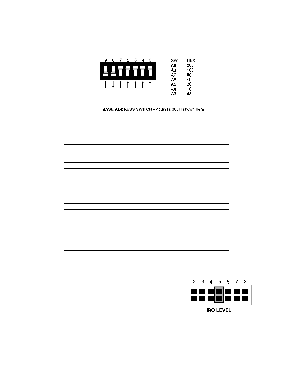
Weights 200h and 100h are active, totalling a 300h base address. Table 2-1 lists PC I/O addresses and
their uses.
Figure 2-1. Base Address Switches
Table 2-1. PC I/O Addresses
FUNCTIONHEX
RANGE
070-071
CMOS RAM & NMI MASK (AT)
RANGE
2.2.2 INTERRUPT LEVEL SELECT
The interrupt jumper need only be set if the software you are using
requires it. The Universal Library and other programs which take
advantage of the REP-INSW high speed transfer capability of the
board require an interrupt. If you do set the interrupt jumper, please
check your PC's current configuration for interrupt conflicts.
FUNCTIONHEX
EGA2C0-2CF8237 DMA #1000-00F
EGA2D0-2DF8259 PIC #1020-021
GPIB (AT)2E0-2E78253 TIMER040-043
SERIAL PORT2E8-2EF8255 PPI (XT)060-063
SERIAL PORT2F8-2FF8742 CONTROLLER (AT)060-064
PROTOTYPE CARD300-30F
PROTOTTYPE CARD310-31FDMA PAGE REGISTERS080-08F
HARD DISK (XT)320-32F8259 PIC #2 (AT)0A0-0A1
PARALLEL PRINTER378-37FNMI MASK (XT)0A0-0AF
SDLC380-38F8237 #2 (AT)0C0-0DF
SDLC3A0-3AF80287 NUMERIC CO-P (AT)0F0-0FF
MDA3B0-3BBHARD DISK (AT)1F0-1FF
PARALLEL PRINTER3BC-3BFGAME CONTROL200-20F
EGA3C0-3CFEXPANSION UNIT (XT)210-21F
CGA3D0-3DFBUS MOUSE238-23B
SERIAL PORT3E8-3EFALT BUS MOUSE23C-23F
FLOPPY DISK3F0-3F7PARALLEL PRINTER270-27F
SERIAL PORT3F8-3FFEGA2B0-2BF
There is a jumper block on the CIO-DAS800 located just above the
PC bus interface (gold pins). The factory default setting is that no
interrupt level is set. The jumper is in the 'X' position at the factory.
It is shown in Figure 2-2 set for IRQ 5.
2
Figure 2-2. IRQ Jumper Block
Page 7

Table 2-2 lists typical interrupt assignments.
Table 2-2. Typical IRQ Assignments
DESCRIPTIONNAMEDESCRIPTIONNAME
REAL TIME CLOCK (AT)IRQ8PARITYNMI
RE-DIRECTED TO IRQ2 (AT)IRQ9TIMERIRQ0
UNASSIGNEDIRQ10KEYBOARDIRQ1
IRQ2
INT 8-15 (AT)
UNASSIGNEDIRQ11RESERVED (XT)
UNASSIGNEDIRQ12COM OR SDLCIRQ3
80287 NUMERIC CO-PIRQ13COM OR SDLCIRQ4
HARD DISKIRQ14HARD DISK (XT) LPT (AT)IRQ5
UNASSIGNEDIRQ15FLOPPY DISKIRQ6
Note: IRQ8-15 are AT onlyLPTIRQ7
2.2.3 WAIT STATE
A wait state can be enabled on the CIO-DAS800 by selecting WAIT STATE ON at the jumper provided
on the board. Enabling the wait state causes the personal computer's bus transfer rate to slow down
whenever the CIO-DAS800 is written to or read from. The wait state jumper is provided in case you one
day own a personal computer with an I/O bus transfer rate which is too fast for the CIO-DAS800. If your
board fails sporadically in random ways, try setting the wait state ON.
2.2.4 INSTALLING THE CIO-DAS800 IN THE COMPUTER
1. Turn the power off.
2. Remove the cover of your computer. Please be careful not to dislodge any of the cables installed
on the boards in your computer as you slide the cover off.
3. Locate an empty expansion slot in your computer.
4. Push the board firmly down into the expansion bus connector. If it is not seated fully it may fail
to work and could short circuit the PC bus power onto a PC bus signal. This could damage the
motherboard in your PC as well as the board.
5. Power up your computer and run the InstaCal test to verify your hardware installation.
3
Page 8

3 CONNECTOR DIAGRAM
The CIO-DAS800 analog connector is a 37-pin, D-type connector accessible from the rear of the PC
through the expansion backplate (Figure 3-1). The connector accepts female 37-pin D-type connectors,
such as those on the C37FF-2, a 2-foot cable with connectors.
If frequent changes to signal connections or signal conditioning is required, please refer to the
information on the CIO-TERMINAL and CIO-MINI37 screw terminal boards, CIO-EXP32, 32 channel
analog MUX/AMP. Isolation amplifiers can be mounted using the ISO-RACK08 and 5B isolation
modules.
Figure 3-1. Analog Connector
WARNING - PLEASE READ
Measure the voltage between the ground signal at the signal source and the PC. Use a
high input impedance voltmeter. If there more the 10 volts, do not connect the
CIO-DAS800 to this signal source because you will not be able to make a reading. If the
difference is more than 30 volts, DO NOT connect this signal to the CIO-DAS800
because IT WILL DAMAGE the board and possibly the computer.
4
Page 9

4 OPERATIONAL ASPECTS - CIO-DAS800 VS. CIO-DAS08
4.1 CONVERSION TRIGGER
A trigger is the event that begins an acquisition/transfer cycle. There are three ways to trigger a
CIO-DAS800; software, interrupt service routine or hardware. The hardware trigger is a new feature on
the CIO-DAS800, not found on the other DAS08 family boards. This new, improved trigger allows the
board to run much faster than the other DAS08 boards.
Briefly, there are three methods to trigger a data conversion:
A software trigger starts an A/D conversion when an addressed port is written to. This is how a single
sample may be taken.
An interrupt service routine is a set of instructions executed by the computer when an interrupt is
received. The source of the interrupt is the IR input pin. The signal on the IR input pin is routed to the
PC bus via the interrupt jumper on the CIO-DAS800. The event that causes the interrupt may be the
internal 82C54 counter or an external event.
The hardware trigger is a direct input to the A/D chip's start conversion pin. When the trigger is
received, the A/D starts a conversion. When the conversion is complete, the data is transferred to the
FIFO buffer. The source for the hardware trigger can be the 82C54 counter/pacer or an external event.
A trigger is useful for synchronizing samples to a known time base, such as the on board 82C54
programmable divider. Using an external trigger allows you to synchronize samples to an external event.
4.2 IMPROVED CHANNEL SEQUENCER
When the acquisition strategy you set up requires a scan of data from multiple channels, the channel
sequencer controls the internal multiplexer that routes the signal to the A/D. The DAS08 family employs
a register that must be written to each time the mux is incremented.
The improved hardware channel sequencer on the CIO-DAS800 is set up, then takes over control of the
internal multiplexer, freeing the CPU from that task. This gives faster sampling.
4.3 CONTROL REGISTERS
The CIO-DAS800 is compatible with DAS08 software because the basic I/O register have identical
functions on each board. I/O registers are the locations which the computer writes commands and data to
and reads status and data from. Table 1-1 is a summary of board registers. The register at BASE+2 is a
multi-function register. It and the others are described in the register section of this manual.
Table 1-1. Register Summary
FUNCTION Read/ WriteI/O ADDRESS
A/D Low Byte / Start Conv A/DBASE + 0
A/D High Byte / Start Conv A/DBASE + 1
Special Multi-Functions RegisterBASE + 2
Gain & Range Control / StatusBASE + 3
5
Page 10

Read Counter 0/ Load Counter 0BASE + 4
Read Counter 1 / Load Counter 1BASE + 5
Read Counter 2 / Load Counter 2BASE + 6
Status & ID / Counter ControlBASE + 7
4.4 FIFO
The FIFO buffer is 256 bytes deep. A larger FIFO makes higher throughput of A/D conversions possible.
This is important when running Windows, and will be more important in future versions of that OS. This
does not affect compatibility in any way because it is a hardware-only function and is transparent to the
software.
4.5 FIFO HALF-FULL INTERRUPT
In addition to a larger FIFO, the CIO-DAS800 has a 1/2-full interrupt. This means that a transfer request
is made after the CIO-DAS800 accumulates 128 samples instead of after every sample. This greatly
improves throughput. This does not affect compatibility with other similar boards in any way because it
is a hardware function and is transparent to the software.
4.6 WAIT STATE JUMPER
Adding this jumper causes a wait state to be inserted into each CPU cycle whenever the CIO-DAS800 is
accessed. This may be necessary on machines with very fast ISA busses, but the need for the wait state is
very rare. This jumper does not affect compatibility in any way because it is a hardware function and is
transparent to the software.
4.7 REFERENCE VOLTAGE
The CIO-DAS800 A/D converter, an AD674, provides a precision 10V reference.
6
Page 11

4.8 SINGLE-ENDED ANALOG INPUTS
The board accepts single-ended inputs only. Each input has two wires connected to the CIO-DAS800; a
channel high (CH# HI) and a Low Level Ground (LLGND). The LLGND signal
ground the PC is on.
The CH# HI is the voltage signal source in the range of +/-5V maximum.
must be the same
4.9 DIGITAL OUTPUTS & INPUTS
The digital inputs and outputs on the CIO-DAS800 are TTL level. TTL is an electronics industry term,
short for Transistor Transistor Logic, which describes a standard for digital signals. For a listing of the
TTL level specifications for these digital lines, please see the specifications at the end of this manual.
There are three digital inputs and four digital outputs. The digital outputs are controlled by a register on
the board and are updated each time the register is written to. The digital inputs are buffered by a
register on the board. Each time the register is read, the current high/low state of the digital I/O lines is
obtained. The lines are pulled high so a one (1) is read when no signal is connected to an input
Typically, the digital lines are used to control external expansion boards (all four outputs) and to trigger
and gate A/D conversions (IP0 input).
4.10 COUNTER TIMER CIRCUIT
There is an 82C54 counter/timer on the board which can be used to:
y
Pace analog conversions
y
Measure frequency
y
Count events
y
Precisely time intervals
The Universal Library has software to support the timer. The connections to the hardware are explained
here. For detailed information on the 82C54 registers, please refer to the Intel or AMD data sheet for this
part if you wish to program the 82C54 registers directly.
The 82C54 contains three counters, each is 16 bits wide. Of the three counters, two are dedicated to
pacing analo-to-digital conversions. These two, CTR1 and CTR2, when not in use by the A/D, are
available for other tasks but are limited to some extent by access to I/O pins. The first counter, CTR0, is
available for user applications.
7
Page 12

C
22
ALL
10K
2
4
+5VDC+5VD
10 MHZ CRYSTAL
OSCILLATOR
DIVIDE BY
10
CLK 0
GATE 0
GATE 1
CLK 1
GATE 2
CLK 2
82C54
CASCADE
CONTROL
LOGIC
OUT 0
OUT 1
OUT 2
CTR 0 OUT
CTR 1 OUT
3
5
CTR 2
OUT
6
START CONVERT
PACE R
CONTROL
LOGIC
DIN 1/
TRIG
25
INT INPUT /
XCLK
24
Figure 1-1. Counter/Timer Functional Diagram
Figure 1-1 shows the 82C54 functions, I/O pins and how these are connected on the CIO-DAS800.
The CIO-DAS800 CTR2 input is connected to the PC bus clock/2 or the 1 MHz. crystal signal. The
system default is the PC bus clock.
Software controls the counters that generate the A/D pacing pulse.
Note: A/D conversions are triggered by falling-edge signals. The pulses generated by the 82C54 are
low-going for one count length. The A/D is triggered as the signal goes low. Any A/D trigger signal you
supply externally must also be low-going at the desired moment of A/D conversion.
8
Page 13

5 REGISTER MAP
)
Tables 4-1 and 4-2 contain the write and read functions of the board’s registers. Table 4-3 defines the
functions of each bit.
Note that the register at BASE + 2 is a multi-function register. Its function is set by bits CS0 and CS1 in
BASE + 3 register. Coding for Base + 02 register functions is contained in Table 4-4.
Table 4-5 gives the Gain Select codes for the CIO-DAS800.
NOTE: ONLY +/-5V IS SUPPORTED.
Table 4-6 provides special programming instructions.
Table 4-1. Register Map - Write Functions
FunctionData BitsWRITE
Functions
D0D1D2D3D4D5D6D7
Base + 2
Base + 4
Base + 5
Base + 6
Base + 7
Special Function
CS0,1
8254 C/T 0 Control Register
8254 C/T 1 Control Register
8254 C/T 2 Control Register
8254 Counter/Timer Control Register
- (Depends on value of
ENHFCS0CS1CSEBase + 3
R1R2R3
* Writing (anything) to either BASE + 0 or BASE + 1 starts a conversion.
Base + 0
Base + 1
MA0MA1MA2INTEOP1OP2OP3OP4CS1/0=0/0
SC0SC1SC2EC0EC1EC2NANACS1/0=1/0
Start Conversion
Start Conversion*
Control Register 1
ITECASCDTENIEOCEACSGTENNAHCENCS1/0=0/1
Conversion Control
Scan Limits Register
Control Select
R0
A/D Timer
Cascade Pre-scaler
Register
*
9
Page 14

Functions
Register
Table 4-2. Register Map - Read Functions
FunctionData BitsREAD
D0D1D2D3D4D5D6D7
FFEMFFOVFF2FF3AD0AD1AD2AD3Base + 0
Low byte read
AD4AD5AD6AD7AD8AD9AD10AD11Base + 1
High byte read
MA0MA1MA2IRQIP1IP2IP3EOCBase + 2
Status Register 1
MA0MA1MA2EACSBase + 3
R1R2R3
R0
Control Status
Base + 4
8254 C/T 0 Status Register
Base + 5
8254 C/T 1 Status Register
Base + 6
8254 C/T 2 Status Register
Base + 7
Function depends on value of CS0/1 bits in Base +3:
CS1/0=
0/0,0/1,1/0
CS1/0 = 1/1
ITECASCDTENDTIEOCINTEGTENHCEN
Status Register 2
ID Reg (ID1,0 = 0/0)ID0ID1ID2ID3ID4ID5ID6ID7
10
Page 15

DEFINITIONS:
AD 11:0
MA2:0
INTE
EOC
HCEN
GTEN*
EACS*
IEOC
DTEN*
CASC*
ITE*
CSE
CS1:0
R3:0
ENHF*
DT*
FFEM*
FFOV*
FF2*
FF3*
SC2:0*
EC2:0*
IP3:1
OP4:1
RW
RW
RW
RW
RW
RW
RW
RW
RW
RW
Table 4-3. Bit Definitions
Analog data input (Read low byte first)
R
Mux address bits
Interrupt enable (0 = disable, 1 = enable)
End-of-conversion (1 = busy, 0 = ready)
R
Gate Enable (Req. DTEN to enable HW gate)
Enable Auto channel-scan
Interrupt Source (1 = End of Convert, 0 = Ext)
Cascade AD Pacing Mode Enable (include CT/2)
Internal Time Base (8254) Enable
W
Register Select Enable/Range Select Disable
W
Register Selection (See Table Below)
(N/A)
Enable Interrupt on FIFO Half Full (Req. IEOC=1, HCEN must =1 to enable
W
FIFO)
R
State of Digital Trigger (1=Trigger occured)
R
FIFO Empty =1. 0 if HCEN =0.
R
0 if HCEN =0. 0 if HCEN =1 & FIFO not empty. Undefined if HCEN = 1 and FIFO
R
empty
0 if HCEN =0. 0 if HCEN =1 & FIFO not empty. Undefined if HCEN = 1 and FIFO
R
empty
Channel-scan start value.
W
Channel-scan end value
W
Digital Input bits.
R
W
Digital Output bits.
FIFO Overflow (full) =1. 0 if HCEN =0.
* Asterisk indicates that HCEN is required (as a final step) to make
this bit functional.
Hardware Convert Enable
External Digital Trigger Enable (Edge trig if GTEN=0)
11
Page 16

Register
Table 4-4. Coding for Base + 02 Register Functions
Control Register Selected
Read Function Write FunctionCS0CS1
Status Register #2 Control Reg # 100
Status Register #2 Conversion Control10
Status Register #2 Scan Limits Reg01
ID Register Not defined11
Table 4-5. Special Programming Instructions
Special Programming instructions
HCEN is used as a master enable for AD PacingConv/Control
Set HCEN last, by itself (ie write 80h) , set the other bits first
Ending channel (n) can be lower than starting channel (m) : m,...,6,7,0,1,...,n,m...Scan Limits
Select Start and End Channel before setting EACS
ID
Operating
modes
Bit
Only the 1st two bits are needed for software, the upper six are for compatibility with KMB
software
ID 1/0: 0/0= (DAS800], 0/1= reserved, 1/0= N/A, 1/1= N/A)
Not appplicable.Gain/Range
CT/2 divides the 1MHz timebase; AD converts when CT/2 counts to zeroNormalPacing
Cascade
External Interrupt and External (Pacer) Clock are mutually exclusiveINT/XCLK
External Interrupt is rising edge, External Pacer is falling edge
CT/1 decrements each time CT/2 counts to zero; AD converts when CT/1 counts
to zero
Requires DTEN=1, GTEN=0EdgeTriggering
"Gate", Requires DTEN=1, GTEN=0LevelGating
12
Page 17

6 SPECIFICATIONS
Power consumption
+5V quiescent 450 mA typical, 600 mA max
Analog input section
A/D converter type AD674A, Successive Approximation
Resolution 12 bits
Number of channels 8
Input Ranges ±5V fixed
Polarity Bipolar fixed
A/D pacing Programmable: internal counter or external source (IR Input
/ XCLK, falling edge) or software polled
A/D Trigger sources External hardware (Digital In 1 / Trig, rising edge)
Data transfer Interrupt or software polled from 256 sample FIFO buffer
Channel configuration Single-ended
DMA None
A/D conversion time 20 µs
Throughput 50 kHz
Accuracy ±0.01% of full scale ±1 LSB typ, ±0.05% of full scale ±1
LSB max
Differential Linearity error ±0.5 LSB max
Integral Linearity error ±1 LSB
No missing codes (guaranteed) 12 bits
Gain drift (A/D specs) ±50 ppm/°C
Zero drift (A/D specs) ±10 ppm/°C
Common Mode Range ±10V
CMRR @ 60 Hz 70 dB min
Input leakage current (@ 25 deg C) ± 30 nA
Input leakage current (over temperature)±250 nA
Input impedance >1000 Mohm typical
Absolute maximum input voltage ±35V
13
Page 18

Counter section
Counter type 82C54
Configuration 3 down-counters , 16 bit resolution
Counter 0 - independent user counter
Source: external, user connector (Counter 0 In)
Gate: external, user connector (Gate 0)
Output: user connector (Counter 0 Out)
Counter 1 - ADC Pacer Lower Divider or independent user counter
Source: user connector (Counter 1 In) and optionally,
Counter 2 Out, selectable by software
Gate: Programmable, disabled or user connector (Gate 1)
Output: User connector (Counter 1 Out) and optionally to A/D
start convert, software selectable
Counter 2 - ADC Pacer Upper Divider
Source: Internal 1 MHz oscillator
Gate: Programmable, disabled or user connector (Gate 2)
Output: User connector (Counter 2 Out) and optionally to
counter 1 input, software selectable
Clock input frequency 10 MHz max
High pulse width (clock input) 30 ns min
Low pulse width (clock input) 50 ns min
Gate width high 50 ns min
Gate width low 50 ns min
Input low voltage 0.8V max
Input high voltage 2.0V min
Output low voltage 0.4V max
Output high voltage 3.0V min
Crystal oscillator
Frequency 1 MHz
Frequency accuracy 100 ppm
Digital I/O section
Digital type FPGA
Configuration Two ports, 3 input and 4 output
Input low voltage 0.8V max
Input high voltage 2.0V min
Output low voltage (IOL = 4 mA) 0.32V max
Output high voltage (IOH = −4 mA)3.86V min
Absolute maximum input voltage −0.5V , +5.5V
Interrupts Jumper selectable: levels 2, 3, 4, 5, 6, 7 or not connected
Positive-edge triggered
Interrupt enable: Programmable
Interrupt sources: External (IR Input / XCLK), A/D End-of-conversion, A/D FIFO Half-Full
Environmental
Operating temperature range 0 to 50°C
Storage temperature range −20 to 70°C
Humidity 0 to 90% non-condensing
14
Page 19

EC Declaration of Conformity
We, Measurement Computing Corp., declare under sole responsibility that the product:
Analog input board with counters and digital I/OCIO-DAS800
DescriptionPart Number
to which this declaration relates, meets the essential requirements, is in conformity with, and CE marking has been applied according to
the relevant EC Directives listed below using the relevant section of the following EC standards and other normative documents:
EU EMC Directive 89/336/EEC
EU 55022 Class B
EN 50082-1
IEC 801-2
IEC 801-3
IEC 801-4
Carl Haapaoja, Director of Quality Assurance
: Electrostatic discharge requirements for industrial process measurement and control equipment.
: Radiated electromagnetic field requirements for industrial process measurements and control equipment.
: Electrically fast transients for industrial process measurement and control equipment.
: Limits and methods of measurements of radio interference characteristics of information technology equipment.
: EC generic immunity requirements.
: Essential requirements relating to electromagnetic compatibility.
Page 20

Measurement Computing Corporation
10 Commerce Way
Suite 1008
Norton, Massachusetts 02766
(508) 946-5100
Fax: (508) 946-9500
E-mail: info@mccdaq.com
www.mccdaq.com
 Loading...