

Page 1

CIO-DAS16Jr/16
USER’S MANUAL
Revision 4
March, 2001
Page 2

LIFETIME WARRANTY
Every hardware product manufactured by Measurement Computing Corp. is warranted against defects in materials or workmanship for
the life of the product, to the original purchaser. Any products found to be defective will be repaired or replaced promptly.
LIFETIME HARSH ENVIRONMENT WARRANTY
TM
Any Measurement Computing Corp. product which is damaged due to misuse may be replaced for only 50% of the current price. I/O
boards face some harsh environments, some harsher than the boards are designed to withstand. When that happens, just return the
board with an order for its replacement at only 50% of the list price. Measurement Computing Corp. does not need to profit from your
misfortune. By the way, we will honor this warranty for any other manufacture’s board that we have a replacement for!
30 DAY MONEY-BACK GUARANTEE
Any Measurement Computing Corp. product may be returned within 30 days of purchase for a full refund of the price paid for the
product being returned. If you are not satisfied, or chose the wrong product by mistake, you do not have to keep it. Please call for a
RMA number first. No credits or returns accepted without a copy of the original invoice. Some software products are subject to a
repackaging fee.
These warranties are in lieu of all other warranties, expressed or implied, including any implied warranty of merchantability or
fitness for a particular application. The remedies provided herein are the buyer’s sole and exclusive remedies. Neither Measurement
Computing Corp., nor its employees shall be liable for any direct or indirect, special, incidental or consequential damage arising
from the use of its products, even if Measurement Computing Corp. has been notified in advance of the possibility of such damages.
MEGA-FIFO, the CIO prefix to data acquisition board model numbers, the PCM prefix to data acquisition board model numbers,
PCM-DAS08, PCM-D24C3, PCM-DAC02, PCM-COM422, PCM-COM485, PCM-DMM, PCM-DAS16D/12, PCM-DAS16S/12,
PCM-DAS16D/16, PCM-DAS16S/16, PCI-DAS6402/16, Universal Library, InstaCal, Harsh Environment Warranty and
Measurement Computing Corp. are registered trademarks of Measurement Computing Corp.
IBM, PC, and PC/AT are trademarks of International Business Machines Corp. Windows is a trademark of Microsoft Corp. All other
trademarks are the property of their respective owners.
Information furnished by Measurement Computing Corp. is believed to be accurate and reliable. However, no responsibility is
assumed by Measurement Computing Corp. neither for its use; nor for any infringements of patents or other rights of third parties,
which may result from its use. No license is granted by implication or otherwise under any patent or copyrights of Measurement
Computing Corp.
All rights reserved. No part of this publication may be reproduced, stored in a retrieval system, or transmitted, in any form by any
means, electronic, mechanical, by photocopying, recording or otherwise without the prior written permission of Measurement
Computing Corp.
Notice
Measurement Computing Corp. does not authorize any Measurement Computing Corp. product for use in life
support systems and/or devices without the written approval of the President of Measurement Computing Corp.
Life support devices/systems are devices or systems which, a) are intended for surgical implantation into the
body, or b) support or sustain life and whose failure to perform can be reasonably expected to result in injury.
Measurement Computing Corp. products are not designed with the components required, and are not subject to
the testing required to ensure a level of reliability suitable for the treatment and diagnosis of people.
(C) Copyright 2001, Measurement Computing Corp
HM CIO-DAS16Jr_16.lwp
Page 3

TABLE OF CONTENTS
1 INSTALLATION
1.1 BASE ADDRESS
1.2 DMA LEVEL SELECT
1.3 8 OR 16 CHANNEL SELECT
1.4 INSTALLING THE BOARD
2 SIGNAL CONNECTIONS
2.1 CONNECTOR DIAGRAM
2.2 ANALOG INPUTS
2.2.1 Single-Ended Inputs
2.2.2 Differential Inputs
2.2.3 System Grounds and Isolation
2.2.4 Determine Your Ground Type
2.2.5 Systems with Common Grounds
2.2.6 Systems with Common Mode (ground offset) Voltages
2.2.7 Small Common Mode Voltages
2.2.8 Large Common Mode Voltages
2.2.9 CIO-DAS16Jr/16 and Signal Source Have Isolated Grounds
2.3 WIRING CONFIGURATIONS
2.3.1 Common Ground / Single-Ended Inputs
2.3.2 Common Ground / Differential Inputs
2.3.3 Common Mode Voltage < +/-10V/Single-Ended Inputs
2.3.4 Common Mode Voltage < +/-10V/Differential Inputs
2.3.5 Common Mode Voltage > +/-10V
2.3.6 Isolated Grounds / Single-Ended Inputs
2.3.7 Isolated Grounds / Differential Inputs
3 REGISTER ARCHITECTURE
3.1 CONTROL & DATA REGISTERS
3.2 A/D DATA & CHANNEL REGISTERS
3.3 CHANNEL MUX SCAN LIMITS REGISTER
3.4 4-BIT DIGITAL I/O REGISTERS
3.5 STATUS REGISTER
3.6 DMA, INTERRUPT & TRIGGER CONTROL
3.7 PACER CLOCK CONTROL REGISTER
3.8 ANALOG INPUT RANGE REGISTER
3.9 PACER CLOCK DATA & CONTROL REGISTERS
3.10 ANALOG INPUT
3.11 DIGITAL INPUT & OUTPUT
3.12 OUTPUT
3.13 INPUT
4 SPECIFICATIONS
.......................................................................
...................................................................
.................................................................
.............................................................
........................................................
.........................................................
............................................................
..........................................................
................................................................
............................................................
.............................................................
.....................................................
.....................................................
....................................................
....................................................
....................................................
.......................................................
..............................................
................................................
.................................................
..............................................
..............................................
......................................................
...................................................
...............................................
...........................................
....................................................
.............................................................
...........................................
...............................................
................................................
...............................................................
......................................................
.....................................................................
...............................................................
...................................
...............................
...................................
.....................................
......................................
1
1
1
1
2
3
3
3
4
4
5
5
6
6
6
7
7
7
8
8
9
9
9
10
10
11
11
12
13
13
14
14
15
16
16
17
17
17
17
18
Page 4

This page is blank.
Page 5

1.1 SOFTWARE
1 INSTALLATION
Before installing the board, install and run
with your board.
regarding these settings can be found below. Refer to the
instructions.
The CIO-DAS16Jr/16 has one bank of base address-select switches and two single-function switches which must be set
before installing the board in your computer.
Cal will guide you through switch and jumper settings for your board. Detailed information
Insta
Cal. This package is the installation, calibration and test utility included
Insta
Software Installation
manual for
Cal installation
Insta
1.2 BASE ADDRESS
Unless there is already a board in your system that uses address 300
hex (768 decimal), leave the switches as they were set at the factory.
In the example shown in Figure 1-1, the board is set for base address
300h (768 decimal).
Figure 1-1 Base Address Switches
1.3 DMA LEVEL SELECT
The board is shipped with the DMA level switch set to DMA level 1. Unless you
have another board in your system using DMA level 1, leave the DMA level switch in
the level 1 position (Figure 1-2).
Some network boards use DMA and so do some IEEE-488 interface boards. If you
suspect a conflict with another board in the system, change the switch to level 3.
Figure 1-2. DMA Level Select Switch
1.4 8 or 16 CHANNEL SELECT
The analog inputs of the CIO-DAS16Jr/16 can be configured as 8 differential
or 16 single-ended. Using differential inputs allows up to 10 volts of common
mode (ground loop) rejection.
The CIO-DAS16Jr/16 comes from the factory configured for eight differential
inputs. Set it for the number of inputs (and type) you require (Figure 1-3).
Figure 1-3. Channel Number Select Switch
1
Page 6

1.5 INSTALLING THE BOARD
Having configured the board’s switches and jumpers, it is now time to install the board into an ISA slot in the PC.
1. Turn the power off.
2. Remove the cover of your computer. Please be careful not to dislodge any of the cables installed on the boards in your
computer as you slide the cover off.
3. Locate an empty ISA expansion slot in your computer.
4. Push the board firmly down into the expansion bus connector. If it is not seated fully it may fail to work and could
short circuit the PC bus power onto a PC bus signal. This could damage the motherboard or the circuit board.
5. Turn the PC power back on and verify proper installation by running
Manual
for information on running
Insta
Cal.
Cal Test (refer to the
Insta
Software Installation
2
Page 7

2 SIGNAL CONNECTIONS
/
2.1 CONNECTOR DIAGRAM
The CIO-DAS16Jr/16 analog connector is a male 37-pin, D-type connector accessible from the rear of the PC through the
expansion backplate. The signals available are identical to the DAS-16, with the exception of pins 8, 9, 10 and 27 (D/A
signals on the DAS-16, no-connect on the CIO-DAS16Jr/16). Another signal, SS&H OUT, can be accessed at pin 26.
CTR0 GATE
Figure 2-1. Connector Pin-Out
The connector (Figure 2-1) accepts female 37-pin D-type connectors, such as those on the C73FF-2, a 2-foot cable with
connectors.
If frequent changes to signal connections or signal conditioning is required, please refer to the information on the
CIO-MINI37 or CIO-TERMINAL screw terminal boards.
For signal conditioning and channel expansion, refer to the information on CIO-EXP32, a 32 channel analog
multiplexer/amplifier; CIO-SSH16, a 16 channel simultaneous sample & hold board or the ISO-RACK16 5B module
interface rack.
2.2 ANALOG INPUTS
Making reliable, trouble-free analog signal connections can be a challenge when using a data acquisition board. The best
method for inputting analog inputs may not be obvious. While a complete coverage of this topic is beyond the scope of
this manual, the following section provides simple explanations and helpful hints. When finished, you should have a
basic understanding of single-ended versus differential inputs and the concepts of system grounding and isolation.
The CIO-DAS16Jr/16 provides either eight differential or 16 single-ended input channels. Descriptions of single-ended
and differential inputs follow.
3
Page 8
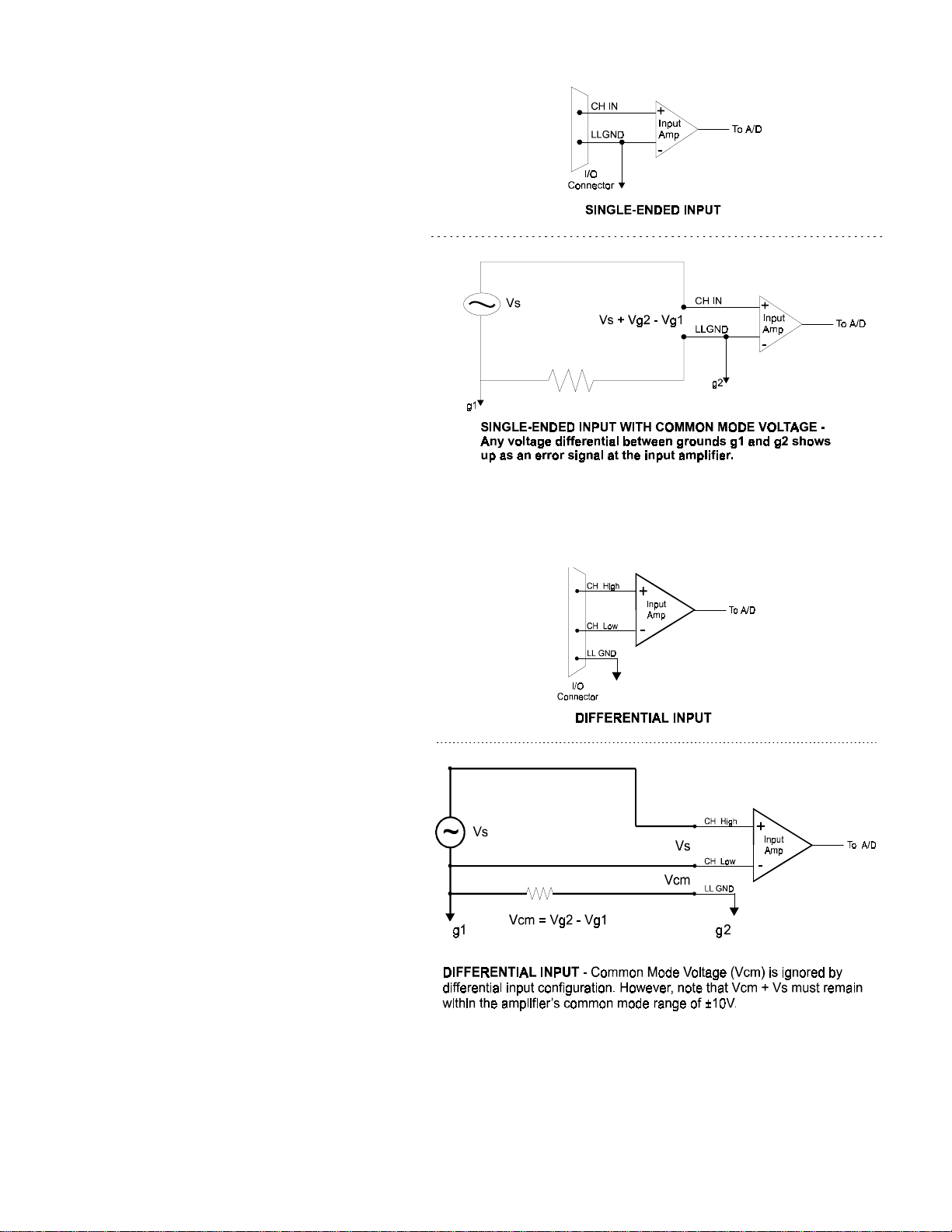
2.2.1 Single-Ended Inputs
In a single-ended input circuit, the voltage
between the input signal terminal and ground is
amplified. In this mode, the CIO-DAS16JR/16
amplifies the voltage between the selected input
channel CH IN and LLGND. The single-ended
input configuration requires only one physical
connection (wire) per channel and allows the
CIO-DAS16JR/16 to monitor more channels
than the (2-wire) differential configuration using
the same connector and on-board multiplexer
(not shown). However, since the circuit is
measuring the input voltage relative to its own
low level ground, single-ended inputs are more
susceptible to both EMI (Electro Magnetic
Interference) and any ground noise at the signal
source. Figure 2-2 shows the single-ended input
configuration.
Figure 2-2. Single-Ended Input Theory
2.2.2 Differential Inputs
In differential input circuits, the voltage between
two distinct input signals is amplified. Within a
certain range (referred to as the common mode
range), the measurement is almost independent of
signal source to CIO-DAS16JR/16 ground
variations. A differential input is also much more
immune to EMI than a single-ended one. Most EMI
noise induced in one lead is also induced in the
other, the input only measures the difference
between the two leads, and the EMI common to
both is ignored. This effect is a major reason there
is twisted pair wire as the twisting assures that both
wires are subject to virtually identical external
influence. Figure 2-3 shows a theoretical
differential input configuration. Note: Multiplexing
is not shown for simplification.
Figure 2-3. Differential Input Theory
4
Page 9

Before describing grounding and isolation, it is important to understand the concepts of common mode, and common
mode range. Common mode voltage is depicted in the diagram above as Vcm. Though differential inputs measure the
voltage between two signals, without (almost) respect to the either signal’s voltages relative to ground, there is a limit to
how far away from ground either signal can go. Though the CIO-DAS16JR/16 has differential inputs, it will not measure
the difference between 100V and 101V as 1 Volt (in fact the 100V would destroy the board!). This limitation or common
mode range is depicted graphically in the following diagram. The CIO-DAS16JR/16 common mode range is +/- 10 Volts.
Even in differential mode, no input signal can be measured if it is more than 10V from the board’s low level ground
(LLGND).
+13V
+12V
+11V
+10V
+9V
+8V
+7V
+6V
+5V
+4V
+3V
+2V
+1V
-1V
-2V
-3V
-4V
-5V
-6V
-7V
-8V
-9V
-10V
-11V
-12V
-13V
With Vcm= +5VDC,
+Vs must be less than +5V, or the common mod e range w ill be e x c eeded (>+10V)
Vcm (Common M ode Voltage) = +5 Volts
Figure 2-4. Common Mode Range Diagram
2.2.3 System Grounds and Isolation
Gray area represents common m ode range
Both V+ and V- must always re ma in w it h in
the common m ode range re la tiv e to L L Gn d
Vcm
There are three conditions possible when connecting the signal source to the board.
1 The board and the signal source may have the same (or common) ground. This signal source can be connected
directly to the board.
2 The board and the signal source may have an offset voltage between their grounds (AC and/or DC). This offset it
commonly referred to a common mode voltage. Depending on the magnitude of this voltage, it may or may not be
possible to connect the board directly to your signal source. We will describe this topic further in a later section.
3 The board and the signal source may already have isolated grounds. This signal source can be connected directly to
the board.
2.2.4 Determine Your Ground Type
Perform the following test: Using a battery powered voltmeter1, measure the voltage between the ground signal at your
signal source and ground at your PC. Measure both the AC and DC Voltages.
1
If you do not have a voltmeter, skip the test and read the following three sections. You may be able to identify your system type from the descriptions provided.
5
Page 10

If both AC and DC readings are 0.00 volts, you may have a system with common grounds. However, since voltmeters
will average out high frequency signals, there is no guarantee. Please refer to the section below entitled Common
Grounds.
If you measure a reasonably stable AC and/or DC voltage, your system has an offset voltage between the two grounds.
This offset is referred to as a common mode voltage. Please read the following warning and then proceed to the section
describing Common Mode systems.
WARNING
If either the AC or DC voltage is greater than 10 volts, do not connect the CIO-DAS16JR/16 to this
signal source. You are beyond the boards usable common mode range and will need to either adjust your
grounding system or add special Isolation signal conditioning to take useful measurements. A ground
offset voltage of more than 30 volts will likely damage the CIO-DAS16JR/16 board and possibly your
computer. You must either reconfigure your system to reduce the ground differentials, or purchase and
install special electrical isolation signal conditioning.
Note: An offset voltage greater than 30 volts will not only damage your electronics, but may be
hazardous to your health.
If you cannot obtain a reasonably stable DC voltage measurement between the grounds, or the voltage drifts around
considerably, the two grounds are most likely isolated. The easiest way to check for isolation is to change your voltmeter
to it’s ohm scale and measure the resistance between the two grounds. Turn both systems off prior to taking this
resistance measurement. If the measured resistance is more than 100 KOhm, assume your system has electrically isolated
grounds.
2.2.5 Systems with Common Grounds
In the simplest (but perhaps least likely) case, your signal source will have the same ground as the CIO-DAS16JR/16.
This would typically occur when providing power or excitation to your signal source directly from the CIO-DAS16JR/16.
There may be other common ground configurations, but it is important to note that any voltage between the
CIO-DAS16JR/16 ground and your signal ground is a potential error voltage if you set up your system based on a
common ground assumption.
In general, if your signal source or sensor is not connected directly to an LLGND pin on your CIO-DAS16JR/16, it’s
best to assume that you do not have a common ground even if your voltmeter measured 0.0 Volts. Configure your system
as if there is ground offset voltage between the source and the CIO-DAS16JR/16. This is especially true if you are using
either the CIO-DAS1402/16 or the CIO-DAS1402/12 at high gains, since ground potentials in the sub millivolt range will
be large enough to cause A/D errors, yet will not likely be measured by your handheld voltmeter.
2.2.6 Systems with Common Mode (ground offset) Voltages
The most frequently encountered grounding problem involves grounds that are somehow connected, but have AC and/or
DC offset voltages between the CIO-DAS16JR/16 and signal source grounds. This offset voltage may be AC, DC, or
both, and may be caused by a variety of things including EMI pickup, resistive voltage drops in ground wiring and
connections, etc. Ground offset voltage is a more appropriate term to describe this type of system, but we’ll use the
phrase Common Mode.
2.2.7 Small Common Mode Voltages
Even if the voltage between the signal source ground and CIO-DAS16JR/16 ground is small, the combination of the
ground voltage and input signal still must not exceed the CIO-DAS800’s +/-10V common mode range. (The voltage
between grounds, added to the maximum input voltage, must stay within +/-10V.) If this is the case, the system can safely
be connected without additional signal conditioning. Fortunately, most systems fall in this category and have a small
voltage between grounds.
6
Page 11

2.2.8 Large Common Mode Voltages
If the ground differential is large enough, the CIO-DAS800’s +/- 10V common mode range will be exceeded. In this case
the CIO-DAS16Jr/16 cannot be directly connected to the signal source. You must change your system grounding
configuration or add isolation signal conditioning. (Please look at our ISO-RACK and ISO-5B-series products to add
electrical isolation, or give our technical support group a call to discuss other options).
NOTE
Do not rely on the earth prong of a 120VAC for signal ground connections. Different ground plugs may
have large and potentially even dangerous voltage differentials. Remember that the ground pins on
120VAC outlets on different sides of the room may only be connected in the basement. This leaves the
possibility that the “ground” pins may have a significant voltage differential (especially if the two 120
VAC outlets happen to be on different phases!)
2.2.9 CIO-DAS16Jr/16 and Signal Source Have Isolated Grounds
Some signal sources are already electrically isolated from the CIO-DAS16Jr/16. The diagram below shows a typical
isolated ground system. These signal sources are often battery powered, or are fairly expensive pieces of equipment
(isolation can be expensive). Isolated ground systems provide excellent performance but requires careful design and
installation to assure optimum performance. Please refer to the following sections for further details
2.3 WIRING CONFIGURATIONS
Combining all the grounding and input type possibilities provides us with the following connection configurations.
The combinations along with our recommendations on usage are summarized in Table 2-1 below.
OUR VIEW
RecommendedSingle-Ended InputsCommon Ground
AcceptableDifferential InputsCommon Ground
Not RecommendedSingle-Ended Inputs
RecommendedDifferential Inputs
Unacceptable without
adding Isolation
Unacceptable without
adding Isolation
GROUND
CATEGORY
Common Mode
Voltage < +/-10V
Common Mode
Voltage < +/-10V
Common Mode
Voltage > +/- 10V
Common Mode
Voltage > +/-10V
Table 2-1. Ground Condition/Input Type Compatibility
INPUT
CONFIGURATION
Single-Ended Inputs
Differential Inputs
Already Isolated
Grounds
AcceptableSingle-ended InputsAlready Isolated Grounds
RecommendedDifferential Inputs
7
Page 12

The following sections depicts recommended input wiring schemes for each of the seven possible input
g
g
g
configuration/grounding combinations.
NOTE: For simplicity, the input multiplexers are not shown in the following diagrams.
2.3.1
Common Ground / Single-Ended Inputs
Single-ended is the recommended configuration for common ground connections. However, if some of your inputs are
common ground and some are not, we recommend you use the differential mode. There is no performance penalty (other
than loss of channels) for using a differential input to measure a common ground signal source. However the reverse is
not true. Figure 2-5 below shows a basic connection diagram for a common ground / single-ended input system.
Signal
S our c e w ith
C om m on Gn d
Optional wire
since signal source
and A/D board share
common ground
I/O
Connector
CH IN
LL GND
Signal source and A/D board
sharin
common ground connected
to s in
le- en d e d in p u t.
+
Inp u t
Amp
-
A/D Board
To A / D
.
Figure 2-5
Common Ground / Single-Ended Input
2.3.2 Common Ground / Differential Inputs
The use of differential inputs to monitor a signal source with a common ground is a acceptable configuration though it
requires more wiring and offers half the channels of a single-ended configuration. Figure 2-6 below shows the basic
connections in this configuration.
Signal
So ur ce w ith
Co mm o n G n d
Optiona l w ire
since signal source
and A/D board sha re
common ground
Figure 2-6. Common Ground / Differential Inputs
Required conn ection
of LL GND to CH Low
I/O
Connector
CH High
CH Low
LL GND
Signal source and A/D board
sharin
com m on ground connected
to differential input.
+
Input
Amp
-
A/D Board
To A /D
8
Page 13

2.3.3 Common Mode Voltage < +/-10V/Single-Ended Inputs
g
g
Isola t ion
g
g
g
g
g
g
g
g
g
g
g
g
g
g
This is not a recommended configuration. In fact, the phrase common mode has no meaning in a single-ended system and
this case would be better described as a system with offset grounds. Anyway, you are welcome to try this configuration,
no system damage should occur and depending on the overall accuracy you require, you may receive acceptable results.
2.3.4 Common Mode Voltage < +/-10V/Differential Inputs
Systems with varying ground potentials should always be monitored in the differential mode. Care is required to assure
that the sum of the input signal and the ground differential (referred to as the common mode voltage) does not exceed the
common mode range of the A/D board (+/-10V on the CIO-DAS16JR/16). Figure 2-7 below show recommended
connections in this configuration.
Signal Source
w ith Com m o n
Mo d e Vol ta g e
The voltage differential
between these grounds,
added to the maximum
input signal must stay
within +/-10 V
Signal source and A/D board
with common m ode volta
connected to a differential input.
GND
I/O
Connector
CH Hi
CH Low
LL GND
h
+
Inp ut
Amp
-
A/D Board
To A / D
e
Figure 2-7
2.3.5 Common Mode Voltage > +/-10V
.
Common Mode Voltage < +/-10V/Single-Ended Inputs
The CIO-DAS16JR/16 will not directly monitor signals with common mode voltages greater than +/-10V. You will either
need to alter the system ground configuration to reduce the overall common mode voltage, or add isolated signal
conditioning between the source and your board (Figure 2-8).
Isola tio n
Barrier
arge common
L
mode voltage
betw ee n sign al
s o urce & A /D bo ard
GND
When the voltage difference
nal source and
between si
A/D board
rou nd is la rge
h so the A/D boa rd’s
enou
common mode ran
exceeded, isolated si
conditionin
e is
nal
must be added.
I/O
Connector
CH IN
LL GN D
System with a Large Common M ode Voltage,
Co n n e cte d to a S in
le-Ended Input
+
Inp u t
Amp
-
A/D Board
To A /D
arge common
L
mode voltage
betw ee n signa l
sourc e & A/D bo a rd
Barrier
GND
When the voltage difference
nal source and
between si
round is large
A/D board
enou
h so the A/D board’s
common mode ran
exceeded, isolated si
conditionin
e is
nal
must be added.
10 K
10K is a recommended value. You may short LL GND to CH Low
instead, but this will reduce your system’s noise immunity.
I/O
Connector
CH Hi
CH Low
LL GND
System with a Large Comm on Mode Voltage,
Connected to a Differential Input
h
+
Inpu t
Amp
-
A/D Board
To A / D
Figure 2-8. Common Mode Voltage > +/-10V - Serial/Differential Inputs
9
Page 14

2.3.6 Isolated Grounds / Single-Ended Inputs
g
Single-ended inputs can be used to monitor isolated inputs, though the use of the differential mode will increase you
system’s noise immunity. Figure 2-9 below shows the recommended connections is this configuration
Isolated
signal
s o urc e
CH IN
LL GND
I/O
Connector
+
-
Inpu t
Amp
To A /D
.
A/D Board
Isolated Signal S ource
Connected to a Single-Ended Input
Figure 2-9
.
Isolated Grounds / Single-Ended Inputs
2.3.7 Isolated Grounds / Differential Inputs
Optimum performance with isolated signal sources is assured with the use of the differential input setting. Figure 2-10
below shows the recommend connections is this configuration..
Signal Source
an d A/D Bo a rd
A lread y I s o la te d .
These
rounds are
electrically isolated.
Figure 2-10. Isolated Grounds / Differential Inputs
Already isolated signal source
and A/D board connected to
a differential input.
GND
10 K
10K is a recommended value. You may short LL GND to CH Low
instead, but this will reduce your system’s noise immunity.
CH High
CH Low
LL GND
I/O
Connector
+
Input
Amp
-
A/D Board
To A /D
10
Page 15

3 REGISTER ARCHITECTURE
3.1 CONTROL & DATA REGISTERS
The CIO-DAS16Jr/16 is controlled and monitored by writing to and reading from 16 consecutive 8-bit I/O addresses.
The first address, or BASE ADDRESS, is determined by setting a bank of switches on the board.
Most often, register manipulation is best left to experienced programmers with a specific need for low level control. If
this is the case for you, use the information that follows to write your own code. Otherwise, we strongly suggest you
consider using the Universal Library™ instead.
The register descriptions follow all follow the format:
01234567
A/D15A/D14A/D13A/D12A/D11A/D10A/D9
Where the numbers along the top row are the bit positions within the 8-bit byte and the numbers and symbols in the
bottom row are the functions associated with that bit.
To write to or read from a register in decimal or hexadecimal, the weights in Table 3-1 apply:
A/D16
LSB
Table 3-1. Bit Weights
HEX VALUEDECIMAL VALUEBIT POSITION
110
221
442
883
10164
20325
40646
801287
To write control or data to a register, the individual bits must be set to 0 or 1 then combined to form a Byte. Data read
from registers must be analyzed to determine which bits are on or off.
The method of programming required to set/read bits from bytes is beyond the scope of this manual. It will be covered in
most Introduction To Programming books, available from a book store.
In summary form, board registers and their function are listed in Table 3-2. Within each register are eight bits which can
constitute a byte of data or can be eight individual bit set/read functions.
11
Page 16

Table 3-2. Register Summary
3.2 A/D DATA & CHANNEL REGISTERS
WRITE FUNCTIONREAD FUNCTIONADDRESS
Start A/D FunctionA/D Bits 9 - 16 (LSB) BASE
NoneA/D Bits 1 (MSB) - 8BASE + 1
Channel MUX SetChannel MUX ReadBASE + 2
Digital 4 Bit OutputDigital 4 Bit InputBASE + 3
NoneNoneBASE + 4
NoneNoneBASE + 5
NoneNoneBASE + 6
NoneNoneBASE + 7
NoneStatus EOC, UNI/BIP etc.BASE + 8
Set DMA, INT etcDMA, Interrupt & Trigger ControlBASE + 9
NonePacer clock control register.BASE + 10
Gain controlGain setting read-backBASE + 11
Counter 0 DataCounter 0 DataBASE + 12
CTR 1 Data - A/D Pacer CTR 1 Data - A/D Pacer ClockBASE + 13
CTR 2 Data - A/D Pacer CTR 2 Data - A/D Pacer ClockBASE + 14
Pacer Clock Contol (8254)None. No read back on 8254BASE + 15
BASE ADDRESS
A read/write register.
READ
On read, it contains the 8LSB’s of A/D data.
WRITE
Writing any data to the register causes an immediate A/D conversion.
BASE ADDRESS + 1
MSB
A Read-only register.
01234567
A/D15A/D14A/D13A/D12A/D11A/D10A/D9
A/D16
LSB
01234567
A/D8A/D7A/D6A/D5A/D4A/D3A/D2A/D1
On read the most significant A/D byte is read.
12
Page 17

3.3 CHANNEL MUX SCAN LIMITS REGISTER
BASE ADDRESS + 2
01234567
CH L1CH L2CH L4CH L8CH H1CH H2CH H4CH H8
A read and write register.
READ
The current channel scan limits are read as one byte. The high channel number scan limit is in the most significant 4
bits. The low channel scan limit is in the least significant 4 bits.
WRITE
The channel scan limits desired are written as one byte. The high channel number scan limit is in the most significant
4 bits. The low channel scan limit is in the least significant 4 bits.
Bits 3-0 contain the starting channel number and bits 7-4 contain the ending channel number. If you wanted to scan
channels 1, 2, 3 in that order, you could do so by placing the 3 in bits 7-4 and the 1 in bits 3-0.
NOTE
Every write to this register sets the current A/D channel MUX setting to the number in bits 3-0. See
BASE + 8.
3.4 4-BIT DIGITAL I/O REGISTERS
BASE ADDRESS + 3
DI30000
CTR0
GATE
When read...
READ
The signals present at the inputs are read as one byte, the most significant four bits of which are always zero. Note
that pins 25 (digital input 0) and 24 (digital input 2) have two functions each.
The TRIG function of digital input 0 may be used to hold of the first sample of an A/D set by holding it low (0V)
until you are ready to take samples, which are then paced by the 8254. It can also be used as the source of an external
start conversion pulse, synchronizing A/D conversions to some external event.
When written to..
WRITE
The upper four bits are ignored. The lower four bits are latched TTL outputs. Once written, the state of the inputs
cannot be read back because a read back would read the separate digital input lines (see above).
DI1DI2,
DI0,
TRIG
01234567
13
Page 18

3.5 STATUS REGISTER
BASE ADDRESS + 8
A read mostly, one-function-write register.
READ
EOC = 1, the A/D converter is busy. EOC = 0, it is free.
U/B = 1, the amplifier is in Unipolar mode. U/B = 0, is bipolar.
MUX = 1, Channels are configured 16 single ended. MUX = 0, 8 differential.
INT = 1, an external pulse has been received. INT = 0, the flip-flop is ready to receive a pulse..
There is a flip-flop on the TRIGGER input (pin 25) which will latch a pulse as short as 200 nanoseconds. Once
triggered, this flip-flop must be reset by a write to this register. Your interrupts service routine must do this before
another interrupt trigger can be received.
CH8, CH4, CH2 & CH1 are a binary number between 0 and 15 indicating the channel number that the MUX is
currently set to and is valid only when EOC = 0. The channel MUX increments shortly after EOC = 1 so may be in a
state of transition when EOC = 1. The binary weight of each bit is shown in Table 3-1 above.
01234567
CH1CH2CH4CH8INTMUXU/BEOC
WRITE
A write of any data to this register resets the flip-flop on the pin 25 input and sets the INT bit to 0.
3.6 DMA, INTERRUPT & TRIGGER CONTROL
BASE ADDRESS + 9
IR1IR2IR4INTE
Care
A read and write register.
READ
INTE = 1, Interrupts are enabled. An interrupt generated will be placed on the PC bus interrupt level selected by IR4,
IR2 & IR1. INTE = 0, interrupts are disabled.
IR4, IR2, IR1 are bits in a binary number between 0 and 7 which map interrupts onto the PC bus interrupt levels 2 - 7.
Interrupts 0 & 1 may not be asserted by the CIO-DAS16Jr/16.
01234567
TS0TS1DMADon’t
DMA = 1, DMA transfers are enabled. DMA = 0, DMA transfers are disabled. Note that this bit only allows the
board to assert a DMA request to the PC on the DMA request level selected by the DMA switch. Before this bit is
set to 1, the PC's 8237 (or appropriate) DMA controller chip must be set up.
TS1 & TS0 control the source of the A/D start conversion trigger according to Table 3-3 below.
14
Page 19

Table 3-3. A/D Conversion Source Coding
TS0TS1
Software triggered A/D onlyX0
Start on rising TRIGGER (Digital input 0, Pin 25)01
Start on Pacer Clock Pulse (CTR 2 OUT, no external access)11
3.7 PACER CLOCK CONTROL REGISTER
BASE ADDRESS + 10
TRIG0CTR0XXXXXX
Write only
CTR0 = 1. When CTR0 = 1, an on-board 100 kHz lock signal is ANDed with the COUNTER 0 CLOCK INPUT (pin
21). A high on pin 21 will allow pulses from the on-board source into the 82C54 Counter 0 input.
CTR0 = 0. When CTR0 = 0, the input to 82C54 Counter 0 is entirely dependent on pulses at pin 21, COUNTER 0
CLOCK INPUT.
TRIG0 = 1. When TRIG0 = 1, the TRIGGER input at pin 25 is ANDed with TRIG0 which must therefore be high for
the pulses from the on-board pacer clock (82C54) to start A/D conversions. The input at pin 25 is pulled up and will
always be high unless pulled low externally.
01234567
TRIG0 = 0. When TRIG0 = 0, the GATEs of counter 1 & 2 are held high, preventing gating of the pacer clock from
pin 25. Reviewing Figure 3-1 may help in understanding the functions of these registers.
+5V
+5V
CONTROL REGISTER
CONTROL REGISTER
BASE + 10
BASE + 10
TRIG
TRIG
CTR0
0
CTR0
1/10
1/10
10 MHz
10 MHz
CIO-DAS16 8254 PACER CLOCK & CONTROL
CIO-DAS16 8254 PACER CLOCK & CONTROL
+5V
10K
10K
GATE
GATE
GATE
GATE
GATE
GATE
+5V
+5V
10K
10K
+5V
10K
10K
COUNTER 0
COUNTER 0
COUNTER 1
COUNTER 1
COUNTER 2
COUNTER 2
A/D PACER
A/D PACER
OUT
OUT
OUT
OUT
OUT
OUT
24
24
21
21
20
20
25
25
2
2
GATE 0
GATE 0
CTR 0 IN
CTR 0 IN
CTR 0 OUT
CTR 0 OUT
CTR 2 OUT
CTR 2 OUT
TRIGGER
TRIGGER
Figure 3-1. Pacer Control Logic
15
Page 20

3.8 ANALOG INPUT RANGE REGISTER
BASE ADDRESS + 11
Table 3-4. Range Coding
01234567
G0G1Uni/BipXXXXX
G0G1UNI/BIP
RANGE
READ or WRITE
A write to this register sets the analog input range for all 8/16 analog inputs. The lower three bits set the analog input
range (Table 3-4). The upper five bits are not used.
To set the analog input range of the CIO-DAS16Jr/16 programmatically, write the correct input range code to the base
address + 11. For example, from BASIC:
If the board's base address is 300h (768 decimal), then the gain register is at 768 + 11 = 779
OUT 779, 5 'Set analog output range to 0 to 5V
The decimal range codes are in the far right column above.
DECIMALINPUT
0±10V000
1±5V100
2±2.5V010
3±1.25V110
40 to 10V001
50 to 5V101
60 to 2.5V011
70 to 1.25V111
3.9 PACER CLOCK DATA & CONTROL REGISTERS
8254 COUNTER 0 DATA
BASE ADDRESS + 12
8254 COUNTER 1 DATA
BASE ADDRESS + 13
8254 COUNTER 2 DATA
BASE ADDRESS + 14
01234567
D1D2D3D4D5D6D7D8
01234567
D1D2D3D4D5D6D7D8
01234567
D1D2D3D4D5D6D7D8
16
Page 21

The three 8254 counter/timer data registers may be written to and read from. Because each counter will count as high as
65,535, it is clear that loading or reading the counter data must be a multi-step process. Refer to the 8254 data sheet
http://www.measurementcomputing.com/PDFmanuals/82C54.pdf for details regarding the programming of the 8254
counter / timer.
82C54 COUNTER CONTROL
BASE ADDRESS + 15
WRITE ONLY
This register controls the operation and loading/reading of the counters. Refer to the 8254 data sheet
http://www.measurementcomputing.com/PDFmanuals/82C54.pdf for details regarding the programming of the 8254
counter / timer.
at
at
01234567
D1D2D3D4D5D6D7D8
3.10 ANALOG INPUT
Analog signals connected to P1, the 37D connector which protrudes from the expansion slot of the PC, are first fed into
the two HI-0508 analog multiplexers. A multiplexer's (MUX) function is to select one of several (8) inputs and connect
that input to the MUX output. MUX U5 connects CH0-CH7 high inputs. MUX U9 connects CH0-CH7 Low input
(differential input mode) or CH8-CH15 High inputs (single-ended mode) depending on the state of the channel
configuration switch located at the upper right of the board and marked 8/16.
From the output of the MUX, the analog signal is fed into a programmable differential amplifier.
The A/D converter chip has an integral sample & hold circuit, greatly simplifying design and improving signal integrity.
The A/D converter is capable of sampling rates to 100 kHz but the DMA transfer circuitry of the personal computer's
8-bit bus may limit the transfer rate to less than the maximum A/D rate. Therefore, the maximum sampling rate of the
CIO-DAS16Jr/16 is dependent on the computer.
3.11 DIGITAL INPUT & OUTPUT
There are four bits of output-only and four bits of input-only on the CIO-DAS16Jr/16 analog connector. From the
original DAS-16 design, these were the only eight bits of digital I/O.
3.12 OUTPUT
The output bits are part of chip U20, a 74LS197 output buffer. The other half of the chip is used for on-board control. If
the digital output lines are blown by overload or high voltage connection, you can replace this chip.
3.13 INPUT
The input bits are part of chip U23, a 74LS244 buffer. The other half of this chip is used for on board functions. This
chip is socketed.
17
Page 22

4 SPECIFICATIONS
POWER CONSUMPTION
+5V quiescent 850 mA typical, 1250 mA max
ANALOG INPUT SECTION
A/D converter type AD7805PB
Resolution 16 bits
Number of channels 8 differential or 16 single-ended (switch-selectable)
Input ranges ±10V, ±5V, ±2.5V, ±1.25V, 0 to 10V, 0 to 5V, 0 to 2.5V, 0 to
1.25V, fully programmable
Polarity Unipolar/Bipolar programmable, 11 ms max switching delay
A/D pacing Programmable: internal counter or external source (DIG. IN 0 / TRIGGER,
rising edge) or software polled
A/D Trigger sources External polled gate trigger (DIG. IN 0 / TRIGGER, active high)
A/D Triggering Modes
Digital: Gated pacer, software polled. (Gate must be disabled by software after trigger
event.)
Data transfer DMA, interrupt or software polled
DMA Channels 1 and 3, switch-selectable
DMA enable Programmable
A/D conversion time 10 µs
Throughput 100 kHz typical, PC dependent
Absolute accuracy 0.0023% of reading ±1.5 LSB
Differential Linearity error +1.5/-1 LSB
Integral Linearity error ±1.5 LSB
No missing codes (guaranteed) 16 Bits
Gain drift (A/D specs) ±10 ppm/°C
Zero drift (A/D specs) ±5 ppm/°C
Common Mode Range ±10V
CMRR @ 60 Hz −96 dB
Input leakage current (@ 25 deg C) 200 nA
Input impedance 30 MegΩ
Absolute maximum input voltage ±35V
DIGITAL I/O SECTION
Digital type
Output 74LS197
Input 74LS244
Configuration 4 fixed input, 4 fixed output
Number of channels 8
Output High 2.7 volts min @ −0.4 mA
Output Low 0.5 volts max @ 8 mA
Input High 2.0 volts min, 7 volts absolute max
Input Low 0.8 volts max, −0.5 volts absolute min
Interrupts Programmable: levels 2 thru 7
Interrupt enable Programmable
Interrupt sources A/D End-of-conversion, DMA terminal count
18
Page 23

COUNTER SECTION
Counter type 82C54
Configuration 3 down counters, 16 bits each
Counter 0 - independent, available to user
Source: programmable: external (CTR0 Clock In) or 100 kHz internal
Gate: programmable: external (Dig In 2 / Ctr 0 Gate, active high) or disabled
Output: Available at user connector (CTR 0 Out)
Counter 1 - ADC Pacer Lower Divider
Source: 10 MHz internal
Gate: Tied to Counter 2 gate, programmable source: internal or external (DIG. IN
0 / TRIGGER).
Output: Chained to Counter 2 Clock.
Counter 2 - ADC Pacer Upper Divider
Source: Counter 1 Output.
Gate: Tied to Counter 1 gate, programmable source: internal or external (DIG. IN
0 / TRIGGER).
Output: ADC Pacer clock, available at user connector (CTR 2 Out)
Clock input frequency 10 Mhz max
High pulse width (clock input) 30 ns min
Low pulse width (clock input) 50 ns min
Gate width high 50 ns min
Gate width low 50 ns min
Input low voltage 0.8V max
Input high voltage 2.0V min
Output low voltage 0.4V max
Output high voltage 3.0V min
Crystal oscillator
Frequency 10 MHz
Frequency accuracy 100 ppm
ENVIRONMENTAL
Operating temperature range 0 to 50°C
Storage temperature range −20 to 70°C
Humidity 0 to 90% non-condensing
19
Page 24

For your notes.
20
Page 25

EC Declaration of Conformity
We, Measurement Computing Corp., declare under sole responsibility that the product:
CIO-DAS16Jr/16
DescriptionPart Number
to which this declaration relates, meets the essential requirements, is in conformity with, and CE marking has been applied according to
the relevant EC Directives listed below using the relevant section of the following EC standards and other normative documents:
EU EMC Directive 89/336/EEC
EU 55022 Class B
EN 50082-1
IEC 801-2
IEC 801-3
IEC 801-4
Carl Haapaoja, Director of Quality Assurance
: Electrostatic discharge requirements for industrial process measurement and control equipment.
: Radiated electromagnetic field requirements for industrial process measurements and control equipment.
: Electrically fast transients for industrial process measurement and control equipment.
: Limits and methods of measurements of radio interference characteristics of information technology equipment.
: EC generic immunity requirements.
: Essential requirements relating to electromagnetic compatibility.
Page 26

Measurement Computing Corporation
16 Commerce Boulevard,
Middleboro, Massachusetts 02346
(508) 946-5100
Fax: (508) 946-9500
E-mail: info@measurementcomputing.com
www. measurementcomputing.com
 Loading...