

Page 1

CIO-DAS1601/12
CIO-DAS1602/12
CIO-DAS1602/16
ANALOG & DIGITAL I/O BOARD
for ISA BUS
Standard and -P5 versions
Revision 6
© Copyright November, 2000
Page 2

LIFETIME WARRANTY
Every hardware product manufactured by Measurement Computing Corp. is warranted against defects in
materials or workmanship for the life of the product, to the original purchaser. Any products found to be
defective will be repaired or replaced promptly.
LIFETIME HARSH ENVIRONMENT WARRANTY
TM
Any Measurement Computing Corp. product which is damaged due to misuse may be replaced for only
50% of the current price. I/O boards face some harsh environments, some harsher than the boards are
designed to withstand. When that happens, just return the board with an order for its replacement at only
50% of the list price. Measurement Computing Corp. does not need to profit from your misfortune. By
the way, we will honor this warranty for any other manufacture’s board that we have a replacement for!
30 DAY MONEY-BACK GUARANTEE
Any Measurement Computing Corp. product can be returned within 30 days of purchase for a full refund
of the price paid for the product being returned. If you are not satisfied, or chose the wrong product by
mistake, you do not have to keep it. Please call for a RMA number first. No credits or returns accepted
without a copy of the original invoice. Some software products are subject to a repackaging fee.
These warranties are in lieu of all other warranties, expressed or implied, including any implied warranty
of merchantability or fitness for a particular application. The remedies provided herein are the buyer’s
sole and exclusive remedies. Neither Measurement Computing Corp., nor its employees shall be liable
for any direct or indirect, special, incidental or consequential damage arising from the use of its products,
even if Measurerment Computing Corp. has been notified in advance of the possibility of such damages.
MEGA-FIFO, the CIO prefix to data acquisition board model numbers, the PCM prefix to data acquisition board model numbers, PCM-DAS08, PCM-D24C3, PCM-DAC02, PCM-COM422, PCM-COM485,
PCM-DMM, PCM-DAS16D/12, PCM-DAS16S/12, PCM-DAS16D/16, PCM-DAS16S/16, PCIDAS6402/16, Universal Library, InstaCal, Harsh Environment Warranty and Measurement Computing
Corp. are registered trademarks of Measurement Computing Corp.
IBM, PC, and PC/AT are trademarks of International Business Machines Corp. Windows is a trademark
of Microsoft Corp. All other trademarks are the property of their respective owners.
Information furnished by Measurement Computing Corp. is believed to be accurate and reliable. However, no responsibility is assumed by Measurement Computing Corp. neither for its use; nor for any
infringements of patents or other rights of third parties, which may result from its use. No license is
granted by implication or otherwise under any patent or copyrights of Measurement Computing Corp.
All rights reserved. No part of this publication may be reproduced, stored in a retrieval system, or transmitted, in any form by any means, electronic, mechanical, by photocopying, recording or otherwise without the prior written permission of Measurement Computing Corp.
Measurement Computing Corp. does not authorize any Measurement Computing Corp. product for use in
life support systems and/or devices without the written approval of the President of Measurement Computing Corp. Life support devices/systems are devices or systems which, a) are intended for surgical
implantation into the body, or b) support or sustain life and whose failure to perform can be reasonably
expected to result in injury. Measurement Computing Corp. products are not designed with the components required, and are not subject to the testing required to ensure a level of reliability suitable for the
treatment and diagnosis of people
HM CIO-DAS160#_1#.lwp
Notice
.
Page 3

Table of Contents
1 INTRODUCTION ................................................................
2 SOFTWARE INSTALLATION .....................................................
3 HARDWARE INSTALLATION ....................................................
4 CONNECTOR PINOUTS ..........................................................
5 ANALOG CONNECTIONS ........................................................
6 REGISTER ARCHITECTURE ....................................................
7 CALIBRATION AND TEST ......................................................
8 ANALOG ELECTRONICS .......................................................
1
1
1
13.1 BASE ADDRESS .............................................................
23.2 DMA LEVEL SELECT .........................................................
23.3 1/10 MHz XTAL JUMPER ......................................................
23.4 8/16 CHANNEL SELECT .......................................................
33.5 D/A CONVERTER REFERENCE JUMPER BLOCK .................................
33.6 BIPOLAR/UNIPOLAR AND GAIN SETTING ......................................
43.7 PACER EDGE SELECT ........................................................
53.8 BURST MODE GENERATOR ...................................................
53.9 DT-CONNECT ...............................................................
6
64.1 MAIN CONNECTOR DIAGRAM ................................................
74.2 DIGITAL I/O CONNECTOR (NOT APPLICABLE TO -P5 VERSIONS) .................
8
85.1 ANALOG INPUTS ............................................................
85.1.1 Single-Ended and Differential Inputs ..........................................
115.1.2 System Grounds and Isolation ...............................................
135.2 Wiring Configurations .........................................................
145.2.1 Common Ground / Single-Ended Inputs .......................................
145.2.2 Common Ground / Differential Inputs ........................................
145.2.3 Common Mode Voltage < +/-10V / Single-Ended Inputs ..........................
155.2.4 Common Mode Voltage < +/-10V / Differential Inputs ...........................
155.2.5 Common Mode Voltage > +/-10V ............................................
165.2.6 Isolated Grounds / Single-Ended Inputs .......................................
175.2.7 Isolated Grounds / Differential Inputs ........................................
175.3 ANALOG OUTPUTS .........................................................
19
196.1 CONTROL & DATA REGISTERS ..............................................
206.1.1 A/D DATA & CHANNEL REGISTERS (CIO-DAS1600/12) ........................
216.1.2 A/D DATA & CHANNEL REGISTERS (CIO-DAS1602/16) ........................
216.1.3 CHANNEL MUX SCAN LIMITS REGISTER ...................................
226.1.4 FOUR BIT DIGITAL I/O REGISTERS ........................................
226.1.5 D/A REGISTERS .........................................................
236.1.6 STATUS REGISTER ......................................................
246.1.7 DMA, INTERRUPT & TRIGGER CONTROL ...................................
246.1.8 PACER CLOCK CONTROL REGISTER .......................................
266.1.9 PROGRAMMABLE GAIN CONTROL REGISTER / BURST RATE ..................
276.1.10 PACER CLOCK DATA & CONTROL REGISTERS .............................
276.1.11 24-bit DIGITAL I/O REGISTERS (not applicable on -P5 versions) .................
296.1.12 CONVERT DISABLE REGISTER ...........................................
296.1.13 BURST MODE ENABLE REGISTER ........................................
306.1.14 DAS1600 MODE ENABLE REGISTER ......................................
306.1.15 BURST STATUS REGISTER ...............................................
31
317.1 REQUIRED EQUIPMENT .....................................................
317.2 CALIBRATING THE A/D & D/A CONVERTERS ..................................
32
328.1 VOLTAGE DIVIDERS ........................................................
Page 4

Table of Contents
9 SPECIFICATIONS ..............................................................
338.2 LOW PASS FILTERS .........................................................
34
349.1 CIO-DAS1601/12 & CIO-DAS1602/12 ...........................................
369.2 CIO-DAS1602/16 ............................................................
Page 5
1 INTRODUCTION
The installation and operation of all CIO-DAS1600 series boards are very similar. Throughout this
manual we use CIO-DAS1600 as a generic designation for the CIO-DAS1601/12, CIO-DAS1602/12, and
CIO-DAS1600/16. When required, due to the differences in the boards, the specific board name is used.
2 SOFTWARE INSTALLATION
We recommend you install and run the InstaC
shipped with your board prior to installing the board in your computer. InstaC
TM
installation, test and calibration utility that was
al
TM
will show you how to
al
properly set the switches and jumpers on the board prior to physically installing the board in your
computer.
Refer to the Software Installation Manual for detailed instructions regarding the installation of the
TM
InstaC
al
software.
3 HARDWARE INSTALLATION
The CIO-DAS1600 has a variety of switches and jumpers to set before installing the board in your
computer. By far the simplest way to configure your board is to use the Insta
TM
part of your CIO-DAS1600 software package. Insta
will show you all available options, how to
Cal
configure the various switches and jumpers to match your application requirements, and will create a
configuration file that your application software (and the Universal Library) will refer to so the software
you use will automatically know the exact configuration of the board.
Please refer to the Software Installation Manual regarding the installation and operation of Insta
The following hard copy information is provided as a matter of completeness, and will allow you to set
the hardware configuration of the CIO-DAS1600 board if you do not have immediate access to
TM
Insta
and/or your computer.
Cal
TM
program provided as
Cal
Cal
TM
.
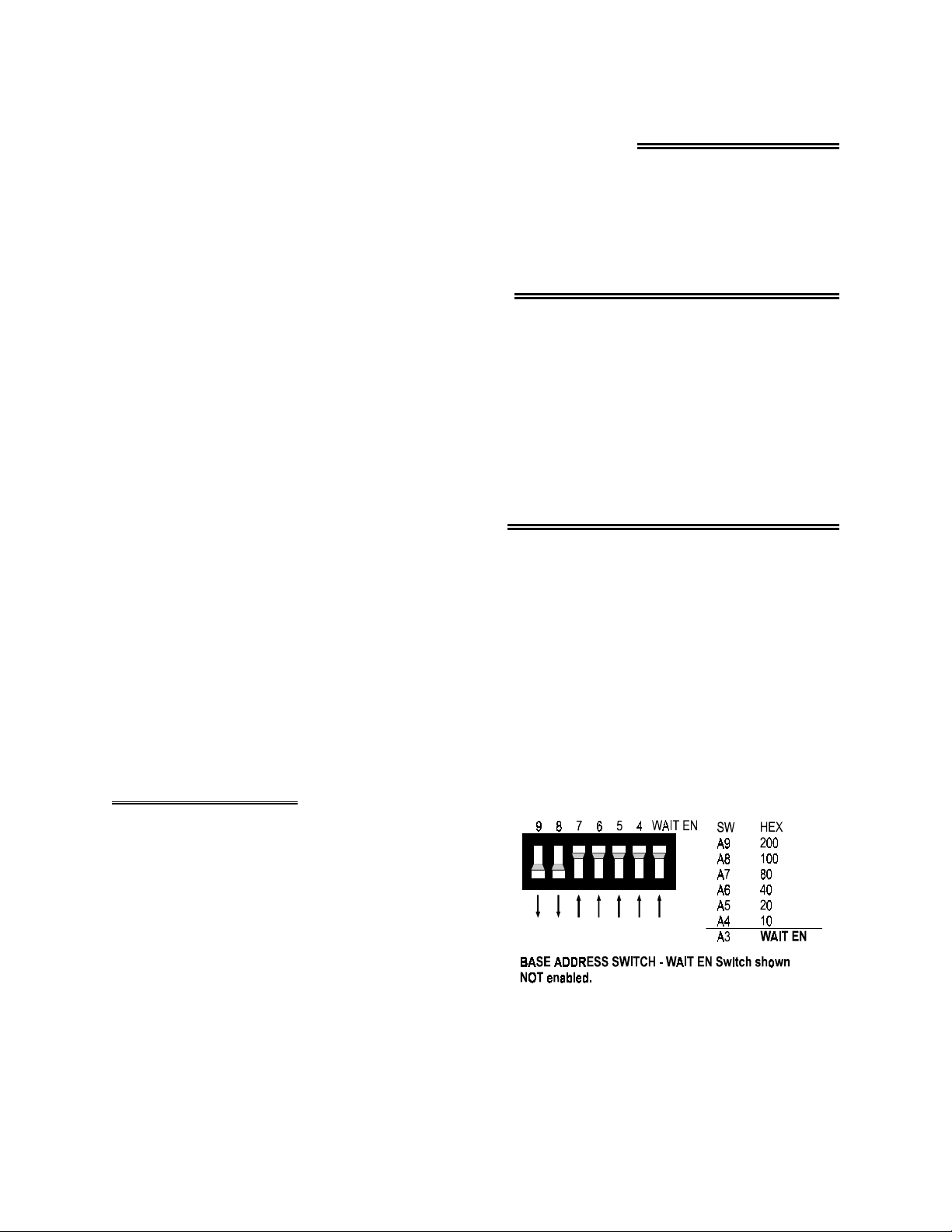
3.1 BASE ADDRESS
Unless there is already a board in your system using
address 300 hex (768 decimal), leave the switches as they
are set at the factory.
In Figure 3-1, the CIO-DAS1600 is set at base address
300 hex. This means the DAS-16 compatible section of
the board is at 300 hex and the DIO-24 compatible
section of the board is at 700 hex.
Figure 3-1. Base Address & Wait EN Switch
Note: Wait State Enable is typically not required. Leave the WAIT EN switch in the UP (not enabled)
position
1
Page 6
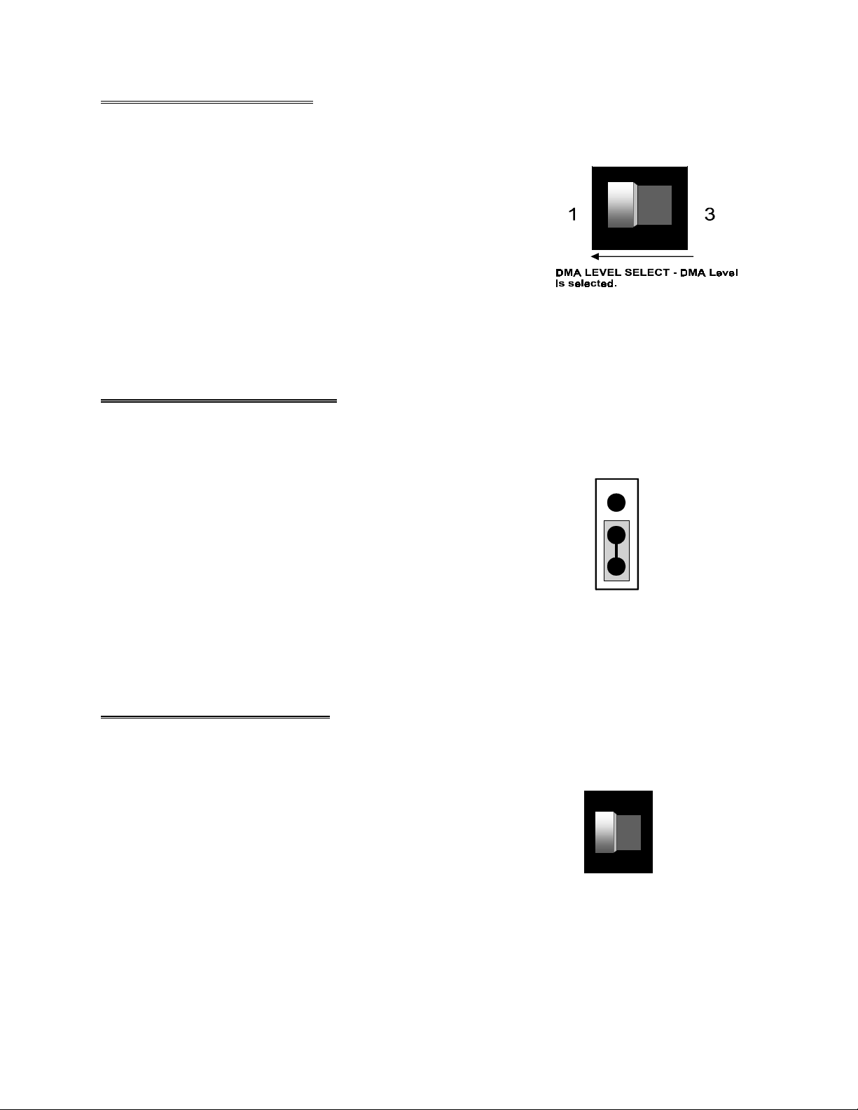
3.2 DMA LEVEL SELECT
1
1
1
If you are installing the board in an old XT bus computer, DMA level 3 is
probably used by the hard disk controller. Set the DMA level switch
to level 1 position (Figure 3-2).
If you have a 386 or higher computer, the hard disk controller does
not use either DMA level 1 or 3 so either level can be selected. The
default level is level 1.
Figure 3-2. DMA Level Select Switch
There are other boards that use DMA levels. Some network boards do and so do some IEEE-488
interface boards. Check to see if you have other boards in your computer that use DMA channels 1 or 3.
3.3 1/10 MHz XTAL JUMPER
The 1/10 MHz XTAL jumper selects the frequency of the square wave
used as a clock by the A/D pacer circuitry. This pacer circuitry controls
the sample timing of the A/D. The output driving the A/D converter is
also available at the CTR 2 output pin on the main connector.
10
To maintain full compatibility with the original DAS-16, the
CIO-DAS1600 required a 1 MHz crystal oscillator. When the DAS-16
was redesigned, a faster 10MHz crystal was added. A jumper is
provided to maintain compatibility with older software. The
CIO-DAS1600 has the jumper because the DAS-16 has the jumper and
some existing software requires the jumper to be in the 1 MHz position
while other software requires a 10 MHz oscillator. The CIO-DAS1600
is shipped with the jumper in the 1 MHz position (Figure 3-3).
Figure 3-3. 1 or 10 MHz Select Jumper
Default 1MHz Show n
CLK SEL
1
3.4 8/16 CHANNEL SELECT
The analog inputs of the CIO-DAS1600 can be configured as eight differential or 16 single-ended. Use
the single-ended input mode if you have more than eight analog
inputs to sample. Using the differential input mode allows up to
10 volts of common mode (ground loop) rejection and will
provide better noise immunity.
The CIO-DAS1600 comes from the factory configured for 16
single-ended inputs and the 8/16 switch is in the position shown in
Figure 3-4. Set it for the type and number of inputs you desire.
This switch is located under the metal shield. If you need access
to this switch, this shield may be removed by removing the two
screws on the back of the CIO-DAS1600.
Figure 3-4. 8/16 Channel Select Switch
6
6/8 CHANNEL SELECT SWITCH
Channel
6-
Single-Ended I
M
ode Shown
8
nput
2
Page 7
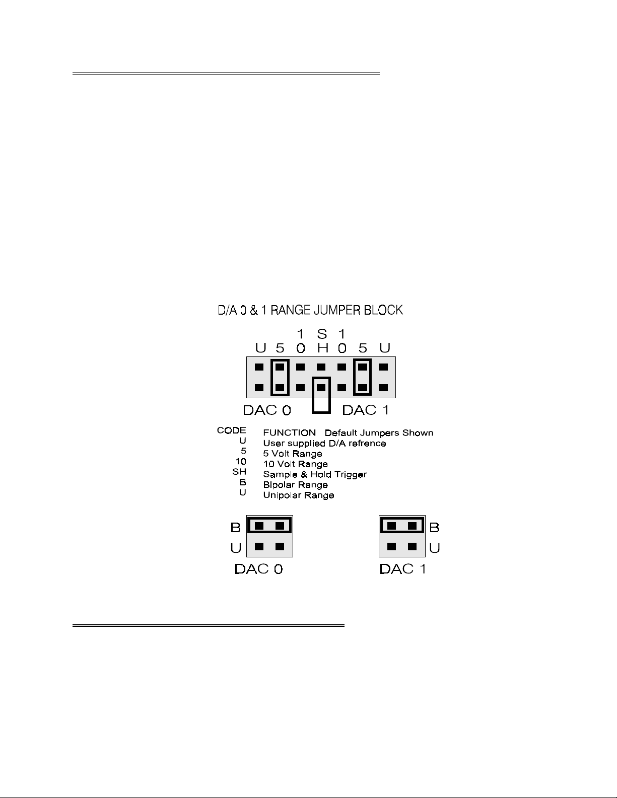
3.5 D/A CONVERTER REFERENCE JUMPER BLOCK
The jumper block located near the center of the CIO-DAS1600 allows you to use the on board precision
voltage reference to select the output ranges of the digital to analog converters.
Analog output is provided by two 12-bit multiplying D/A converters. This type of converter accepts a
reference voltage and provides an output proportional to that. The proportion is controlled by the D/A
output code (0 to 4095). Each bit represents 1/4096 of full scale.
A precision −5V and −10V reference provide onboard D/A ranges of 0 to 5V, 0 to 10V, ±5V, ±10V.
Other ranges between 0V and 10V are available if you provide a precision voltage reference at pin 10 or
26 of the main connector.
When the DAC0 reference is supplied onboard, pin 26 of the 37 pin connector is unused and can be
employed as a simultaneous sample & hold trigger for use with the CIO-SSH16. To do so, place the
jumper between the two pins SH (Figure 3-5).
Figure 3-5. D/A Output Range Jumper Block
3.6 BIPOLAR/UNIPOLAR AND GAIN SETTING
The Bipolar or Unipolar configuration of the A/D converter is set by a switch (Figure 3-6). The switch
controls all A/D channels. Though you cannot run some channels bipolar and some unipolar, you can
measure a unipolar input in the bipolar mode. (e.g. you can monitor a 0 to 5V input with a ±5 V channel)
3
Page 8

The input amplifier gain is controlled by a software programmed register located at BASE + B hex (11
decimal). The codes have different meaning for each board in the CIO-DAS1600 family. Refer to the
Register Architecture section for details on this register.
Figure 3-6. Bipolar/Unipolar Select Switch
3.7 PACER EDGE SELECT
The original Keithley MetraByte DAS-1600 was designed such that A/D conversion was initiated on the
falling edge of the convert signal. Neither the original DAS-16, nor any of the other DAS-16 derivative
converts on the falling edge. In fact, we are not aware of any A/D board that uses the falling edge to
initiate the A/D conversion.
When using the falling edge to start the conversion, the A/D may be falsely triggered by 8254 pacer clock
initialization glitching (easy to avoid but a real possibility in the DAS-1600). Converting on the falling
edge mode also may lead to timing differences if the CIO-DAS1600 board is being used as a replacement
for an older DAS16 series board.
Because using the falling edge trigger is undesirable, we have designed a jumper into the CIO-DAS1600
which allows you to choose which edge of the internal pacer signal
starts the A/D conversion. The jumper has no effect on an external
pacer signal (EXTCLOCK). The only reason we supply you the
option of a falling edge trigger is to provide complete compatibility
TRIGGER EDGE SELECT
JUMPER BLOCK
Falling Edge A/D Trigger
DAS-1600 Method
for those who have developed software for a DAS-1600 using the
AS-1600 drivers, AND, when using the CIO-DAS1600 with that
J9
software you observe sample timing differences.
Rising Edge A/D Trigger
The CIO-DAS1600 is shipped with this jumper in the rising edge
position. Figure 3-7 to the right shows the edge selection options.
For compatibility with all third party packages, with all DAS-16
J9
DAS-16 Method
Default
Setting
software and with CIO-DAS1600 software, leave this jumper in the
rising edge position
Figure 3-7. Trigger Edge Select Jumper
AUXILIARY TRIGGER
There is a position for a header connector at the rear of the CIO-DAS1600. This connector provides the
same function as that found on the DAS-1600.
The A/D trigger signal can come from this connector, if installed. A jumper controls which pin the
trigger signal comes in from. We do not install this connector (nor is it installed on the DAS-1600).
4
Page 9
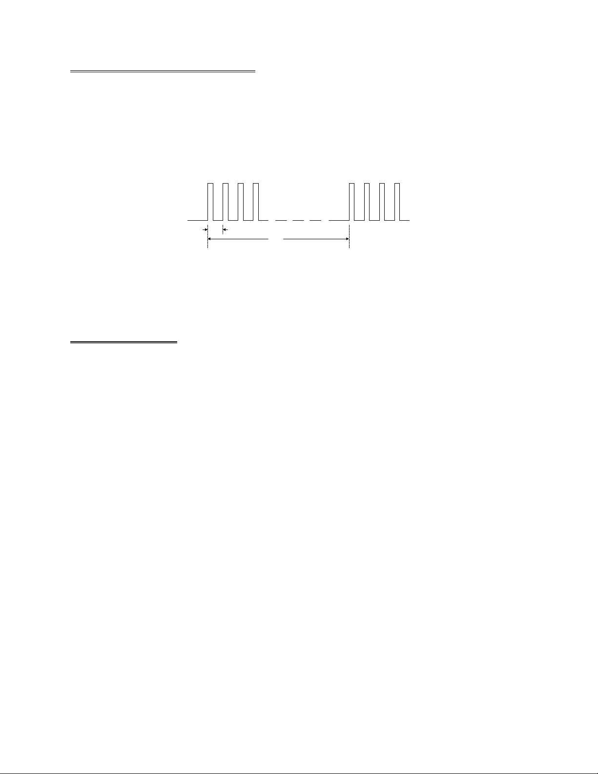
3.8 BURST MODE GENERATOR
The burst mode generator is a clock signal that paces the A/D at the maximum multi-channel sample rate,
then periodically, performs additional maximum rate scans. In this way, the channel to channel skew
(time between successive samples in a scan) is minimized without taking a large number of undesired
samples (Figure 3-8).
.
Ch0 Ch1 Ch2 Ch3
4uS
The length of the delay between
bu rsts is se t b y o n e o f the inte rn a l
cou n ter s o r m a y be co n tro lled v ia
exte rn a l trigge r.
Figure
Delay
. Burst Mode Timing
3-8
Ch0 Ch1 Ch2 Ch3
Burst mode pacer fixed at
4 uS - CIO-DAS1600/12
13.3 uS - CIO-DAS1600/16
The CIO-DAS1600 burst mode generator takes advantage of the fast A/D. The burst mode skew is 4 µs
between channels for the CIO-DAS160#/12. It is 13.3 µs for the CIO-DAS1602/16.
3.9 DT-CONNECT
There is no hardware configuration or installation required for DT-Connect. Software enables/disables
DT-Connect, and of course, you must have a DT-Connect equipped accessory board, (Measurement
Computing’s MEGA-FIFO, for example) before using the DT-Connect.
DT-CONNECT IN MASTER MODE ONLY
The CIO-DAS1600 implements DT-Connect MASTER MODE only. DT-Connect is always enabled and
is never busy. The ENABLED and BUSY signal levels are fixed in hardware. Since DT-Connect is
always enabled, any A/D conversions are always transferred out through the DT-Connect port regardless
of the bus transfer method specified. The CIO-DAS1600 can only operate in DT-Connect schemes where
it is the sole master.
To assure that DT-Connect is properly initialized prior to any A/D transfer, the DT-Connect DT-Request
handshake line is reset each time the programmable gain (Base + 11 decimal) register is written to.
Therefore, it is not possible to use the DT-Connect for A/D sets which involve setting the gain between
samples. This is not really a problem because any such scheme would be low speed and therefore store
data to disk, obviating the need to use DT-Connect to store data on the MEGA-FIFO.
Please see the data sheet on the MEGA-FIFO, a 128 million-sample buffer board as an example of a
DT-Connect accessory.
5
Page 10
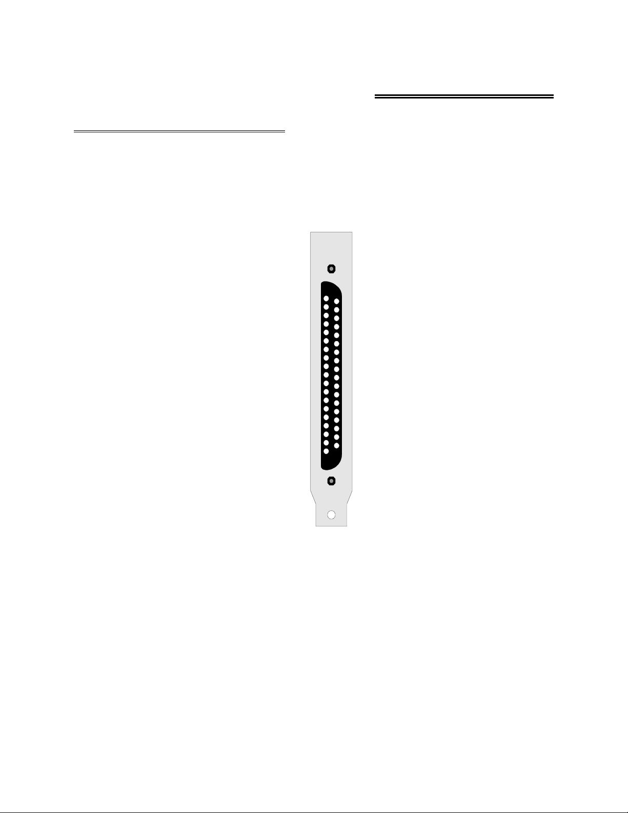
4 CONNECTOR PINOUTS
4.1 MAIN CONNECTOR DIAGRAM
The CIO-DAS1600 analog connector is a 37-pin “D” connector accessible from the rear of the PC
through the expansion back plate. An additional signal, SS&H OUT, is available at pin 26. It is required
when the CIO-SSH16 Simultaneous Sample and Hold card is used with a CIO-DAS1600 (Figure 4-1).
CH0 LOW / CH8 HIGH 18
LLG ND 19
CH1 LOW / CH9 HIGH 17
CH2 LOW / CH10 HIGH 16
CH3 LOW / CH11 HIGH 15
CH4 LOW / CH12 HIGH 14
CH5 LOW / CH13 HIGH 13
CH6 LOW / CH14 HIGH 12
CH7 LOW / CH15 HIGH 11
D/ A 0 RE F IN 10
D/A 0 OUT 9
-5V REF OU T 8
DIG GND 7
DI G IN 1 6
DI G IN 3 5
DIG. OUT 1 4
DIG. OUT 3 3
CTR 0 OUT 2
+5V PC BUS 1
37 C H 0 H IGH
36 C H 1 H IGH
35 C H 2 H IGH
34 C H 3 H IGH
33 C H 4 H IGH
32 C H 5 H IGH
31 C H 6 H IGH
30 C H 7 H IGH
29 LLGND
28 LLGND
27 D /A 1 OU T
26 D /A 1 R E F IN / SS &H O U T
25 DIG IN 0 / TR IGGE R
24 D IG IN 2 / C T R 0 GAT E
23 D IG OUT 0
22 D IG OUT 2
21 CTR 0 CLOCK IN
20 C T R 2 O U T
37 PIN CONNECTOR
Figure 4-1. Main Analog Connector Pinout
The connector accepts female 37-pin D-type connectors, such as those on the C73FF-2, two foot cable
with connectors. If frequent changes to signal connections or signal conditioning is required we strongly
recommend purchasing the CIO-MINI37 screw terminal board and the mating C37FF-2 cable
6
Page 11
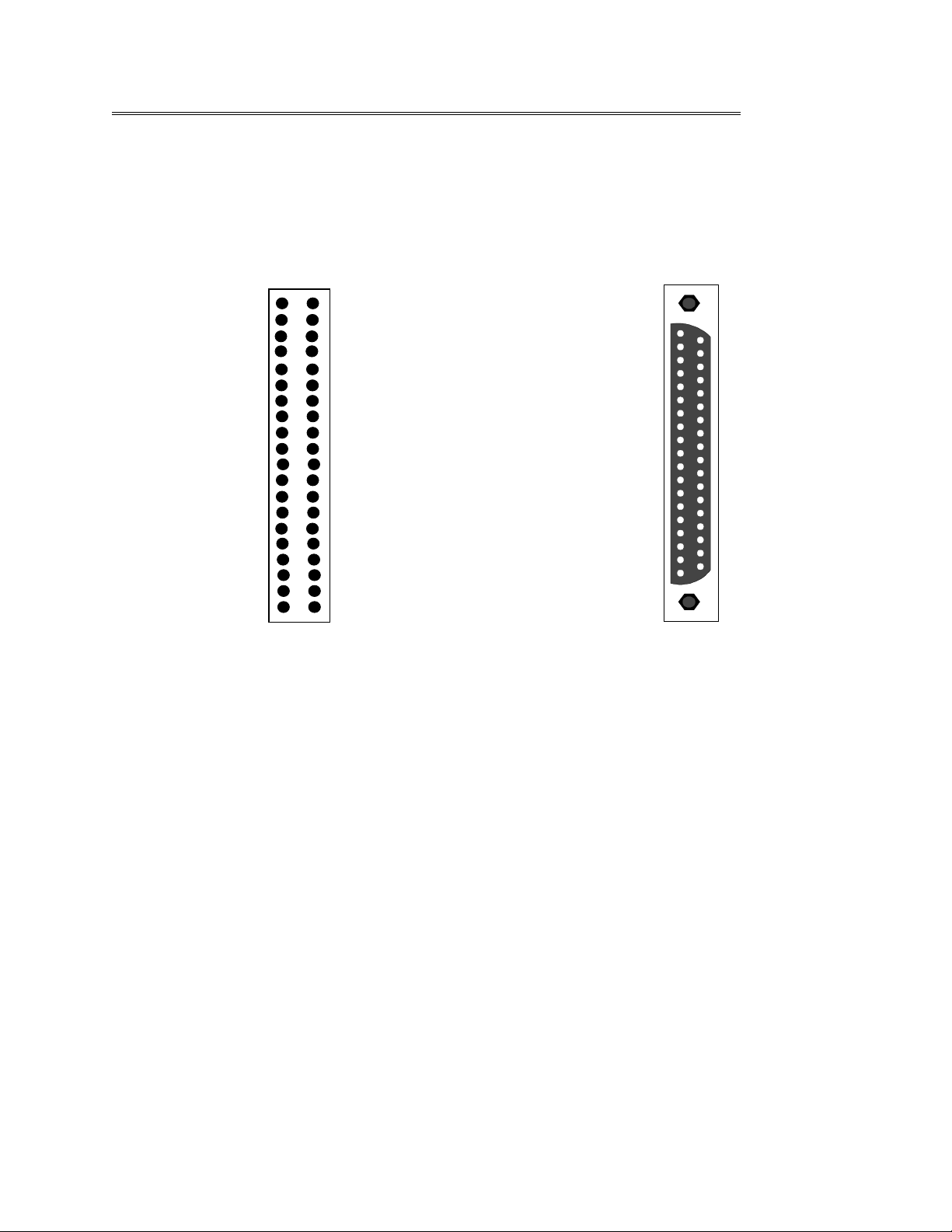
4.2 DIGITAL I/O CONNECTOR (NOT APPLICABLE TO -P5 VERSIONS)
P
P
P
P
P
P
P
P
The digital I/O connector is mounted at the rear of the CIO-DAS1600 and will accept a 40-pin header
connector. The optional BP40-37 cable assembly brings the signals to a back plate with a 37-pin male
connector mounted in it. When connected through the BP40-37, the CIO-DAS1600 digital connector is
identical to the CIO-DIO24 connector. The pin out of the 40- pin digital connector and the BP40-37 cable
assembly are shown in Figure 4-2 below.
NC 40
NC 38
PORT A0 36
PORT A1 34
PORT A2 32
PORT A3 30
PORT A4 28
PORT A5 26
PORT A6 24
PORT A7 22
PORT C0 20
PORT C1 18
PORT C2 16
PORT C3 14
PORT C4 12
PORT C5 10
PORT C6 8
PORT C7 6
GND
4
+5V 2
39 NC
37 GND
35 +5V
33 GND
31 NC
29 GND
27 NC
25 GND
23 NC
21 GND
19 PORT B0
17 PORT B1
15 PORT B2
13 PORT B3
11 PORT B4
9PORTB5
7PORTB6
5PORTB7
3NC
1 NC
GND
+5V
GND
NC
GND
NC
GND
NC
GND
ORT B 0
ORT B 1
ORT B 2
ORT B 3
ORT B 4
ORT B 5
ORT B 6
ORT B 7
NC
NC
19
18
17
16
15
14
13
12
11
10
PORT A 0
37
PORT A 1
36
PORT A 2
35
34
PORT A 3
33
PORT A 4
32
PORT A 5
31
PORT A 6
30
PORT A 7
29
PORT C 0
PORT C 1
9
8
7
6
5
4
3
2
1
28
27
26
25
24
23
22
21
20
PORT C 2
PORT C 3
PORT C 4
PORT C 5
PORT C 6
PORT C 7
GND
+5V
Figure 4-2. Digital 40-Pin Connector Pinout - BP40-37 Cable Assembly to Back Panel Pinout
7
Page 12
5 ANALOG CONNECTIONS
5.1 ANALOG INPUTS
Analog signal connection is one of the most challenging aspects of applying a data acquisition board. If
you are an Analog Electrical Engineer then this section is not for you, but if you are like most PC data
acquisition users, the best way to connect your analog inputs may not be obvious. Though complete
coverage of this topic is well beyond the scope of this manual, the following section provides some
explanations and helpful hints regarding these analog input connections. This section is designed to help
you achieve the optimum performance from your CIO-DAS1600 series board.
Prior to jumping into actual connection schemes, you should have at least a basic understanding of
Single-Ended/Differential inputs and system grounding/isolation. If you are already comfortable with
these concepts you may wish to skip to the next section (on wiring configurations).
5.1.1 Single-Ended and Differential Inputs
The CIO-DAS1600 provides either eight differential or 16 single-ended input channels.
Single-Ended Inputs
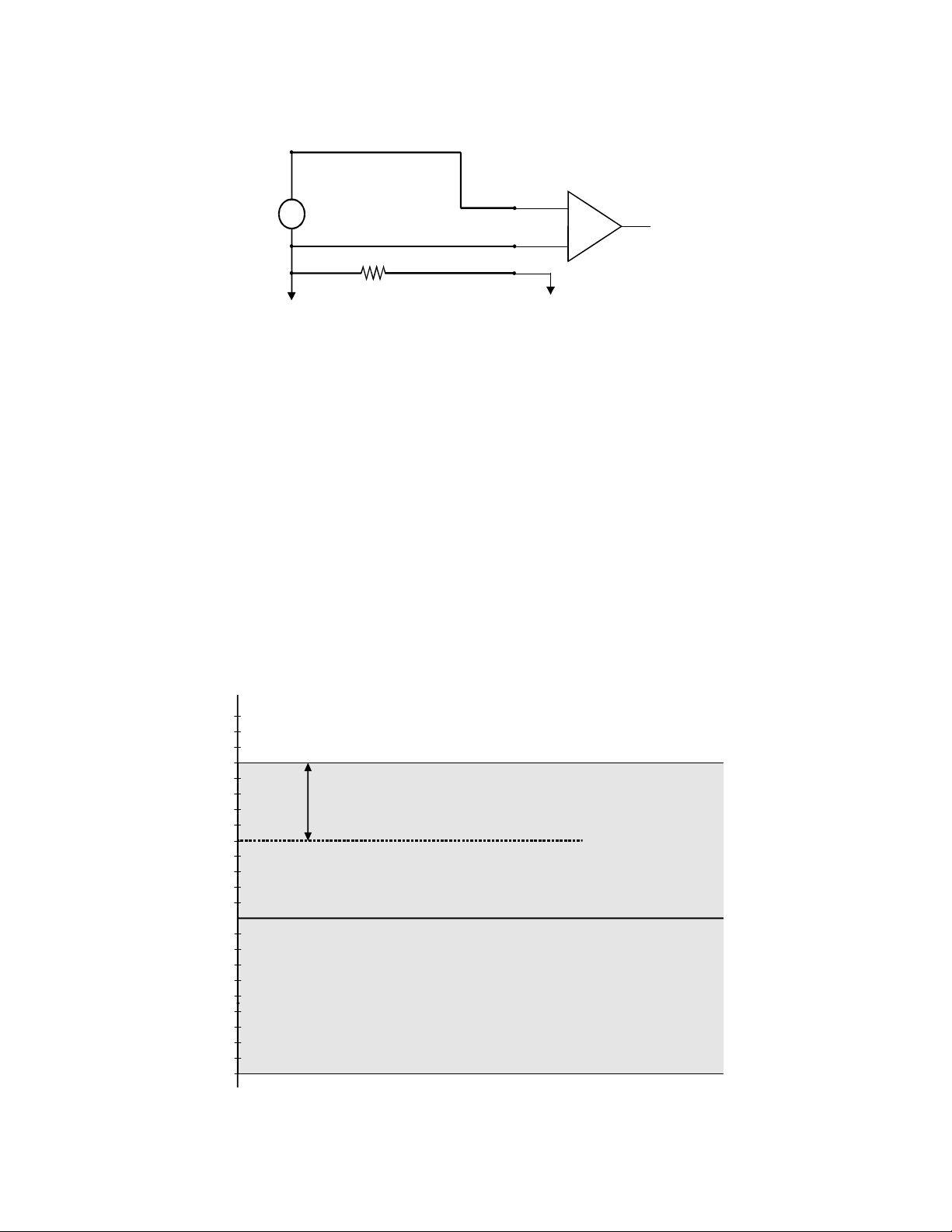
A single-ended input measures the voltage between the input signal and ground. In this case, in
single-ended mode the CIO-DAS1600 measures the voltage between the input channel and LLGND. The
single-ended input configuration requires only one physical connection (wire) per channel and allows the
CIO-DAS1600 to monitor more channels than the (2-wire) differential configuration using the same
connector and onboard multiplexor. However, since the CIO-DAS1600 is measuring the input voltage
relative to its own low level ground, single-ended inputs are more susceptible to both EMI
(Electro-Magnetic Interference) and any ground noise at the signal source. Figure 5-1a and 5-1b show the
theory of single-ended input configuration
CH IN
LL GND
I/O
Connector
+
-
Inp u t
Amp
To A/D
Single-Ended Input
Figure 5-1a. Single-Ended Voltage Input Theory
8
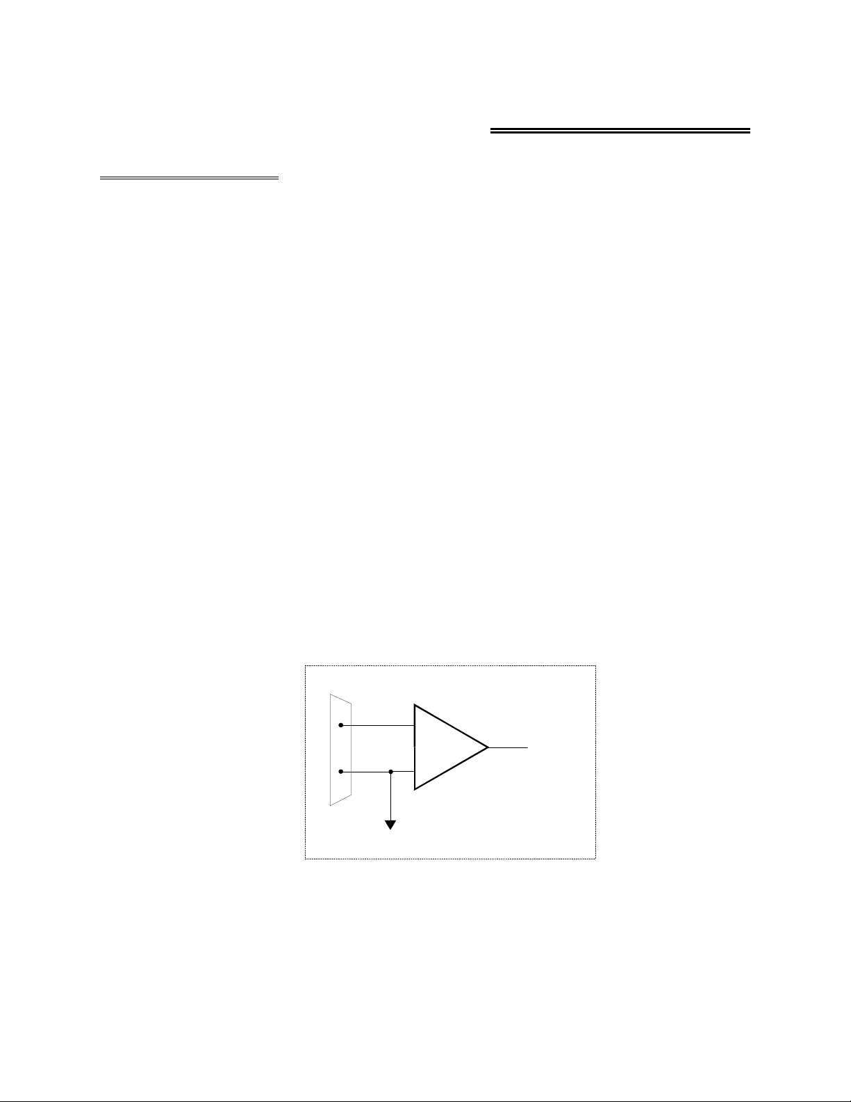
Page 13
~
CH IN
Vs
1
g
Any voltage differential between grounds
g1 and g2 sh ows up as an error signal
at the input amplifier
Vs + Vg2 - Vg1
LL GND
g
2
+
-
Inp u t
Amp
To A /D
Single-ended input with Comm on Mode Voltage
Figure 5-1b. Single-Ended Voltage Input Theory
Differential Inputs
Differential inputs measure the voltage between two distinct input signals. Within a certain range
(referred to as the common mode range), the measurement is almost independent of signal source to
CIO-DAS1600 ground variations. A differential input is also much more immune to EMI than a
single-ended one. Most EMI noise induced in one lead is also induced in the other, the input only
measures the difference between the two leads, and the EMI common to both is ignored. This effect is a
major reason there is twisted pair wire as the twisting assures that both wires are subject to virtually
identical external influence. Figure 5-2a and 5-2b below show a typical differential input configuration.
CH High
CH Low
LL GN D
I/O
Connector
+
Inp ut
Amp
-
Differential Input
Figure 5-2a . Differential Input Theory
9
To A/ D
Page 14
~
Vs
Vs
Vcm
CH High
CH Low
LL GND
+
-
Inp u t
Amp
To A/ D
Vcm = Vg2 - Vg1
Common M ode Voltage (Vcm) is ignored
gg1 2
Differential
Inp u t
by differential inp ut configuration. How ever,
no te th a t Vc m + V s must re ma in within
the amplifier’s com mon m ode range of ±10V
Figure 5-2b. Differential Input Theory
Before moving on to the discussion of grounding and isolation, it is important to explain the concepts of
common mode, and common mode range (CM Range). Common mode voltage is depicted in the diagram
above as Vcm. Though differential inputs measure the voltage between two signals, without (almost)
respect to the either signal’s voltages relative to ground, there is a limit to how far away from ground
either signal can go. Though the CIO-DAS1600 has differential inputs, it will not measure the difference
between 100V and 101V as 1 Volt (in fact the 100V would destroy the board!). This limitation or
common mode range is depicted graphically in Figure 5-3. T he CIO-DAS1600 common mode range is
+/- 10 Volts. Even in differential mode, no input signal can be measured if it is more than 10V from the
board’s low level ground (LLGND).
+13V
+12V
+11V
+10V
+9V
+8V
+7V
+6V
+5V
+4V
+3V
+2V
+1V
W ith V c m= + 5 VDC ,
+Vs mus t be les s t h an +5 V, o r th e c ommo n mo de r an g e will b e ex c eede d ( >+10 V)
Gray area represents com m on m ode ran
Both V+ and V- must always remain withi
the co mmo n m o d e ra n ge re lat ive to L L G
Vcm
-1V
-2V
-3V
-4V
-5V
-6V
-7V
-8V
-9V
-10V
Figure 5-3. Common Mode Range
10
Page 15

5.1.2 System Grounds and Isolation
There are three scenarios possible when connecting your signal source to your CIO-DAS1600 board.
1. The CIO-DAS1600 and the signal source have the same (or common) ground. This signal
source can be connected directly to the CIO-DAS1600.
2. The CIO-DAS1600 and the signal source have an offset voltage between their grounds (AC
and/or DC). This offset it commonly referred to a common mode voltage. Depending on the magnitude
of this voltage, it may or may not be possible to connect the CIO-DAS1600 directly to your signal
source. We will discuss this topic further in a later section.
3. The CIO-DAS1600 and the signal source already have isolated grounds. This signal source
can be connected directly to the CIO-DAS1600.
Which system do you have?
Try the following experiment. Using a battery powered voltmeter*, measure the voltage (difference)
between the ground signal at your signal source and at your PC. Place one voltmeter probe on the PC
ground and the other on the signal source ground. Measure both the AC and DC Voltages.
*If you do not have access to a voltmeter, skip the experiment and take a look a the following three
sections. You may be able to identify your system type from the descriptions provided.
If both AC and DC readings are 0.00 volts, you may have a system with common grounds. However,
since voltmeters will average out high frequency signals, there is no guarantee. Please refer to the section
below titled Common Grounds.
If you measure reasonably stable AC and DC voltages, your system has an offset voltage between the
grounds category. This offset is referred to as a Common Mode Voltage. Please be careful to read the
following warning and then proceed to the section describing Common Mode systems.
WARNING
If either the AC or DC voltage is greater than 10 volts, do not connect the
CIO-DAS1600 to this signal source. You are beyond the boards usable common mode
range and will need to either adjust your grounding system or add special Isolation
signal conditioning to take useful measurements. A ground offset voltage of more
than 30 volts will likely damage the CIO-DAS1600 board and possibly your computer.
Note that an offset voltage much greater than 30 volts will not only damage your
electronics, but it can also be hazardous to your health.
This is such an important point, that we will state it again. If the voltage between the
ground of your signal source and your PC is greater than 10 volts, your board will not
take useful measurements. If this voltage is greater than 30 volts, it will likely cause
damage, and can represent a serious shock hazard! In this case you will need to either
reconfigure your system to reduce the ground differentials, or purchase and install
special electrical isolation signal conditioning.
If you cannot obtain a reasonably stable DC voltage measurement between the grounds, or the voltage
drifts around considerably, the two grounds are most likely isolated. The easiest way to check for
11
Page 16

isolation is to change your voltmeter to it’s ohm scale and measure the resistance between the two
grounds. It is recommended that you turn both systems off prior to taking this resistance measurement. If
the measured resistance is more than 100 Kohm, it’s a fairly safe bet that your system has electrically
isolated grounds.
Systems with Common Grounds
In the simplest (but perhaps least likely) case, your signal source will have the same ground as the
CIO-DAS1600. This would typically occur when providing power or excitation to your signal source
directly from the CIO-DAS1600. There may be other common ground configurations, but it is important
to note that any voltage between the CIO-DAS1600 ground and your signal ground is a potential error
voltage if you set up your system based on a common ground assumption.
As a safe rule of t humb, if your signal source or sensor is not connected directly to an LLGND pin on
your CIO-DAS1600, it’s best to assume that you do not have a common ground even if your voltmeter
measured 0.0 Volts. Configure your system as if there is ground offset voltage between the source and
the CIO-DAS1600. This is especially true if you are using either the CIO-DAS1600/16 or the
CIO-DAS1600/12 at high gains, since ground potentials in the sub-millivolt range will be large enough to
cause A/D errors, yet will not likely be measured by your hand-held voltmeter.
Systems with Common Mode (ground offset) Voltages
The most frequently encountered grounding scenario involves grounds that are somehow connected, but
have AC and/or DC offset voltages between the CIO-DAS1600 and signal source grounds. This offset
voltage may be AC, DC or both and can be caused by a wide array of phenomena including EMI pickup,
resistive voltage drops in ground wiring and connections, etc. Ground offset voltage is a more
appropriate term to describe this type of system, but since our goal is to keep things simple, and help you
make appropriate connections, we’ll stick with our somewhat loose usage of the phrase Common Mode.
Small Common Mode Voltages
If the voltage between the signal source ground and CIO-DAS1600 ground is small, the combination of
the ground voltage and input signal will not exceed the ’CIO-DAS1600’s +/-10V common mode range,
(i.e. the voltage between grounds, added to the maximum input voltage, stays within +/-10V), This input
is compatible with the CIO-DAS1600 and the system can be connected without additional signal
conditioning. Fortunately, most systems will fall in this category and have a small voltage differential
between grounds.
Large Common Mode Voltages
If the ground differential is large enough, the ’CIO-DAS1600’s +/- 10V common mode range will be
exceeded (i.e. the voltage between CIO-DAS1600 and signal source grounds, added to the maximum
input voltage you’re trying to measure exceeds +/-10V). In this case the CIO-DAS1600 cannot be
directly connected to the signal source. You will need to change your system grounding configuration or
add isolation signal conditioning. (Please look at our ISO-RACK and ISO-5B-series products to add
electrical isolation, or give our technical support group a call to discuss other options.)
12
Page 17

NOTE
Relying on the earth prong of a 120VAC for signal ground connections is not advised..
Different ground plugs may have large and potentially even dangerous voltage
differentials. Remember that the ground pins on 120VAC outlets on different sides of
the room may only be connected in the basement. This leaves the possibility that the
“ground” pins may have a significant voltage differential (especially if the two
120VAC outlets happen to be on different phases.)
CIO-DAS1600 and signal source already have isolated grounds
Some signal sources will already be electrically isolated from the CIO-DAS1600. The diagram below
shows a typical isolated ground system. These signal sources are often battery powered, or are fairly
expensive pieces of equipment (since isolation is not an inexpensive proposition), isolated ground
systems provide excellent performance, but require some extra effort during connections to assure
optimum performance is obtained. Please refer to the following sections for further details.
5.2 Wiring Configurations
Combining all the grounding and input type possibilities provides us with the following potential
connection configurations. The combinations along with our recommendations on usage are shown in
Table 5-1 below.
Table 5-1. Input vs. Grounding Recommendations
Ground Category Input Configuration Our Recommendation
RecommendedSingle-Ended InputsCommon Ground
AcceptableDifferential InputsCommon Ground
Common Mode
Voltage < +/-10V
Common Mode
Voltage < +/-10V
Common Mode
Voltage > +/- 10V
Common Mode
Voltage > +/-10V
Single-Ended Inputs
Differential Inputs
Not RecommendedSingle-Ended Inputs
RecommendedDifferential Inputs
Unacceptable without
adding Isolation
Unacceptable without
adding Isolation
AcceptableSingle-ended InputsAlready Isolated Grounds
Already Isolated
Grounds
RecommendedDifferential Inputs
The following sections depicts recommended input wiring schemes for each of the eight possible input
configuration/grounding combinations.
13
Page 18

5.2.1 Common Ground / Single-Ended Inputs
Single-ended is the recommended configuration for common ground connections. However, if some of
your inputs are common ground and some are not, we recommend you use the differential mode. There is
no performance penalty (other than loss of channels) for using a differential input to measure a common
ground signal source. However the reverse is not true. Figure 5-4 below shows a recommended
connection diagram for a common ground / single-ended input system
Signal
S o ur ce w ith
C ommon Gnd
Optional wire
since signa l source
and A/D board share
comm on g round
CH IN
LL GND
I/O
Connector
+
-
Input
Amp
To A /D
A/D Board
Signal source and A/D board
sharing comm on ground connected
to sin gle - e nde d in put.
Figure 5-4. Common Ground / Single-Ended Inputs
5.2.2 Common Ground / Differential Inputs
The use of differential inputs to monitor a signal source with a common ground is a acceptable
configuration though it requires more wiring and offers fewer channels than selecting a single-ended
configuration. Figure 5-5 below shows the recommended connections in this configuration.
Signal
S ou rc e with
Co mm o n Gnd
Optional wire
since signal source
and A/D board share
common g round
Required connection
of LL GND to CH Low
CH High
CH Low
LL GND
I/O
Conn ector
+
Inp u t
Amp
-
A/D Board
To A / D
Signal source and A/D board
sharing comm on ground connected
to differential input.
Figure 5-5. Common Ground / Differential Inputs
14
Page 19

5.2.3 Common Mode Voltage < +/-10V / Single-Ended Inputs
This is not a recommended configuration. In fact, the phrase common mode has no meaning in a
single-ended system and this case would be better described as a system with offset grounds. You can try
this configuration, no system damage should occur and you may receive acceptable results.
5.2.4 Common Mode Voltage < +/-10V / Differential Inputs
Systems with varying ground potentials should always be monitored in the differential mode. Care is
required to assure that the sum of the input signal and the ground differential (referred to as the common
mode voltage) does not exceed the common mode range of the A/D board (±10V on the CIO-DAS1600).
Figure 5-6 below show recommended connections in this configuration.
Signal Source
with Co mm o n
M od e Vo lta g e
The voltage differential
between these grounds,
added to the maximum
input signal mu st stay
w ith in + /- 1 0 V
GND
CH High
CH Low
LL GND
I/O
Conn ector
+
Inp u t
Amp
-
A/D Board
To A /D
Signal source and A/D board
with com m on m ode voltage
connected to a differential input.
Figure 5-6. Common Mode Voltage < +/-10V / Differential Inputs
5.2.5 Common Mode Voltage > +/-10V
The CIO-DAS1600 will not directly monitor signals with common mode voltages greater than +/-10V.
You will either need to alter the system ground configuration to reduce the overall common mode
voltage, or add isolated signal conditioning between the source and your board. See Figure 5-7 and 5-8
below.
Iso la t io n
Barrier
arge common
L
mo de v olta ge
between signal
source & A/D board
When the voltage difference
between signal source and
A/D board ground is large
enough so the A/D board’s
common m ode range is
exceeded, isolated sig nal
conditioning must be added.
System with a Large Com m on M ode Voltage,
GND
Connector
Connected to a Single-Ended Input
I/O
CH IN
LL GND
+
Inpu t
Amp
-
A/D Board
To A /D
Figure 5-7. Common Mode Voltage > +/-10V. Single-Ended Input
15
Page 20

Isol at ion
Barrier
arge common
L
mode voltage
between signal
source & A/D board
When the voltage difference
between signal source and
A/D board ground is large
enough so the A/D board’s
common m ode range is
exceeded, isolated signal
conditioning must be added.
GND
10 K
10K is a recommended value. You may short LL GND to CH L ow
instead, but this will reduce your system’s noise immunity.
System with a Large C om m on M ode Voltage,
Connected to a Differential Input
I/O
Conn ector
CH High
CH Low
LL GND
+
Input
Amp
-
A/D Board
To A / D
Figure 5-8. Common Mode Voltage > +/-10V. Differential Input
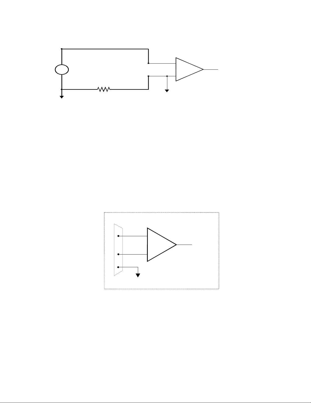
5.2.6 Isolated Grounds / Single-Ended Inputs
Single-ended inputs can be used to monitor isolated inputs, though the use of the differential mode will
increase you system’s noise immunity. Figure 5-9 below shows the recommended connections is this
configuration.
Iso late d
s ign a l
so u rc e
Figure 5-9. Isolated Grounds / Single-Ended Input
CH IN
LL GND
I/O
Conn ector
Iso lated S ignal Source
Connected to a Single-Ended Input
+
Inpu t
Amp
-
A/D Board
To A /D
16
Page 21

5.2.7 Isolated Grounds / Differential Inputs
Optimum performance with isolated signal sources is assured with the use of the differential input
setting. Figure 5-10 below shows the recommend connections is this configuration.
Signal Source
a n d A/D Bo a rd
Alre a dy Is o la te d .
GND
10 K
CH High
CH Low
LL GND
+
-
Inp u t
Amp
To A/ D
These grounds are
electrically isolated.
I/O
Conn ector
10K is a recommended value. You may short LL G ND to CH Low
instead, but this will re d u ce you r system’s noise imm unity.
A/D Board
Already isolated signal source
and A/D board connected to
a differential input.
Figure 5-10. Isolated Grounds / Differential Inputs
5.3 ANALOG OUTPUTS
Analog outputs are simple voltage outputs which can be connected to any device which will record,
display or be controlled by a voltage. The CIO-DAS1600 analog outputs are 4 quadrant multiplying
DACs. This means that they accept an input voltage reference and provide an output voltage which is
inverse to the reference voltage and proportional to the digital value in the output register.
For example, in unipolar mode, the supplied reference of −5V provides a +5V output when the value in
the output register is 4095 (full scale at 12 bits of resolution). It provides a value of 2.5V when the value
in the output register is 2048.
Figure 5-11 shows the onboard reference internally jumpered. Both D/A outputs will have a range of
−5 to +5 volts. This is the default factory configuration.
17
Page 22

Figure 5-11. Analog Output Range Select Jumper Block
18
Page 23

6 REGISTER ARCHITECTURE
There are three common approaches to generating software for the CIO-DAS1600. These are:
1. Writing custom software utilizing our Universal Library package
2. Using a fully integrated software package (e.g. Softwire)
3. Direct register level programming.
CUSTOM SOFTWARE UTILIZING THE UNIVERSAL LIBRARY
Most users write custom software using our Universal Library. The Universal Library takes care of all
the board I/O commands and lets you concentrate on the application part of the software. For additional
information regarding using the Universal Library, please refer to the documentation supplied with the
Universal Library
FULLY INTEGRATED SOFTWARE PACKAGES (e.g. Softwire)
Many users also take advantage of the power and simplicity offered by one of the upper level data
acquisition packages. Please refer to the package’s documentation for setup and usage details.
DIRECT REGISTER LEVEL PROGRAMMING
Although uncommon, some applications do not allow the use of our Universal Library, and are not a
good match for an upper level package. For these situations, detailed register mapping follows. This
chapter is intended for experienced programmers only.
6.1 CONTROL & DATA REGISTERS
The CIO-DAS1600 is controlled and monitored by writing to and reading from 24 distinct I/O addresses.
The first address i s referred to as t he BASE ADDRESS (BADR) and is set by a bank of switches on the
board. All other addresses ar e located at the BASE ADDRESS pl us a specified offset. In partic ular, the
main analog I/O functions are controlled by the I/O addressees from BADR to BADR +15h and BADR
+404h through BADR +407h. The additional 82C55 based digital I/O uses four consecutive I/O
addresses at BASE ADDRESS + 400h (the -P5 versions do not include this 82C55).
Registers are easy to read from and write to, though to create a complete data acquisition software
program at the register level is a significant undertaking. Unless there is a specific reason that you need
to write your program at the register lever, we highly recommend the use of our Universal Library.
The method of programmi ng required to set/read bits from bytes is beyond the scope of this manual. It
will be covered in most Introduction To Programming books, available from a book store. The remainder
of this chapter is included for those experienced programmers who wish to write their own register level
programs.
In summary form, the registers and their functions are listed on Table 6-1 following. Within each
register are eight bits which may constitute a byte of data or be eight individual bit set/read functions.
19
Page 24

BASE + 9
Table 6-1. Register Map
WRITE FUNCTIONREAD FUNCTIONADDRESS
Start A/D ConversionA/D Data (Least significant) BASE
NoneA/D Data (Most significant)BASE + 1
Channel MUX / FIFO resetChannel MUX BASE + 2
Digital 4 Bit OutputDigital 4-Bit InputBASE + 3
D/A 0 Least Significant bitsNoneBASE + 4
D/A 0 Most Significant bitsNoneBASE + 5
D/A 1 Least Significant bitsNoneBASE + 6
D/A 1 Most Significant bitsNoneBASE + 7
Clear InterruptStatus EOC, UNI/BIP etc.BASE + 8
Set DMA, INT etcDMA, Interrupt & Trigger
Control
Burst Length/pacer clk cntrlnoneBASE + Ah
PGA Control/DT resetPGA gain BASE + Bh
Counter 0 DataCounter 0 DataBASE + Ch
CTR 1 Data - A/D PacerCTR 1 Data - A/D Pacer ClockBASE + Dh
CTR 2 Data - A/D PacerCTR 2 Data - A/D Pacer ClockBASE + Eh
Pacer Clock Control (8254)None. No read back on 8254BASE + Fh
Port A Output, n/a on -P5 ver.Port A Input of 8255BASE + 400h
Port B Output, n/a on -P5 ver.Port B InputBASE + 401h
Port C Output, n/a on -P5 ver.Port C InputBASE + 402h
Configure 8255, n/a on -P5 ver.None. No read back on 8255BASE + 403h
Conversion Enable/DisableNoneBASE + 404h
Burst Mode Enable/DisableNoneBASE + 405h
DAS 1600 Enable/DisableNoneBASE + 406h
NoneStatus of extended featuresBASE + 407h
6.1.1 A/D DATA & CHANNEL REGISTERS (CIO-DAS1600/12)
BASE ADDRESS +0
01234567
A/D 1A/D 2A/D 3
CH0CH1CH2CH3A/D 0
LSB
A read/write register.
READ
On read, it contains two types of data. The least significant four digits of the analog input data and the
channel number from which the current data was taken.
These four bits of analog input data must be combined with the eight bits of analog input data in BASE +
1 to form a complete 12-bit number. The data format is 0 = −FS; 4095 = +FS.
The channel number is binary. If the current channel is 5, bits CH2 and CH0 are high, CH3 and CH1 are
low.
WRITE
Writing any data to the register causes an immediate A/D conversion.
20
Page 25

BASE ADDRESS +1
MSB
A Read-only register.
On read the most significant A/D byte is read.
6.1.2 A/D DATA & CHANNEL REGISTERS (CIO-DAS1602/16)
BASE ADDRESS
A/D 1A/D 2A/D 3A/D 4A/D 5A/D 6A/D 7
A read/write register.
READ
On read, it contains the least significant eight digits of the analog input data.
These eight bits of analog input data must be combined with the eight bits of analog input data in
BASE + 1, to form a complete 16-bit number. The data format is 0 = −FS; 65,535 = +FS.
WRITE
Writing any data to the register causes an immediate A/D conversion
.
01234567
A/D 4A/D 5A/D 6A/D 7A/D 8A/D 9A/D 10A/D 11
01234567
A/D 0
LSB
BASE ADDRESS +1
01234567
A/D 8A/D 9A/D 10A/D 11A/D 12A/D 13A/D 14A/D 15
MSB
A Read-only register.
On read the most significant A/D byte is read
.
6.1.3 CHANNEL MUX SCAN LIMITS REGISTER
BASE ADDRESS +2
01234567
CH L0CH L1CH L2CH L3CH H0CH H1CH H2CH H3
A read and write register.
READ
The current channel scan limits are read as one byte. The high channel number scan limit is in the most
significant four bits. The low channel scan limit is in the least significant four bits.
WRITE
The channel scan limits desired are written as one byte. The high channel number scan limit is in the
most significant four bits. The low channel scan limit is in the least significant four bits.
NOTE
Every write to this register sets the current A/D channel MUX setting to the number in
bits 0-3 and resets the FIFO. See BASE + 8.
21
Page 26

6.1.4 FOUR BIT DIGITAL I/O REGISTERS
BASE ADDRESS+3
A read and write register.
When read from...
01234567
DI0, TRIGDI1DI2, CTR0, GATEDI30011
READ
The signals present at the inputs are read as one byte, the most significant four bits of which are always
zero. The pins 25 (digital input 0) and 24 (digital input 2) digital inputs have two functions each.
The TRIG function of digital input 0 can be used to hold off the first sample of an A/D set by holding it
low (0V) until you are ready to take samples, which are then paced by the 8254. It can also be used as
the source of an external start conversion pulse, synchronizing A/D conversions to some external event.
When written to..
01234567
DO0DO1DO2DO3XXXX
WRITE
The upper four bits are ignored. The lower four bits are latched TTL outputs. Once written, the state of
the inputs cannot be read back because a read back would read the separate digital input lines (see
above).
Since the digital inputs have multiple functions, use the digital input lines 0-3 with
care when you are also using the A/D converter.
The digital outputs are also used by the CIO-EXP32, 32-channel analog
multiplexer/amplifier.
6.1.5 D/A REGISTERS
D/A 0 REGISTERS
BASE ADDRESS +4
D/A1D/A2D/A3
BASE ADDRESS + 5
MSB
NOTE
01234567
XXXXD/A0
LSB
01234567
D/A4D/A5D/A6D/A7D/A8D/A9D/A10D/A11
22
Page 27

D/A 1 REGISTERS
BASE ADDRESS + 6
01234567
D/A1D/A2D/A3
XXXXD/A0
LSB
BASE ADDRESS + 7
01234567
D/A4D/A5D/A6D/A7D/A8D/A9D/A10D/A11
MSB
WRITE ONLY
Each 12 bit D/A output line has two registers. The first contains the four least significant bits of the data
and four bits that don't care. The second register contains the eight most significant bits of the data.
The D/A will be updated when the eight most significant bits (upper register) are written. In this way,
the lower four bits can be written with no effect on the D/A output until the remainder of the data is
written to the upper eight bits.
6.1.6 STATUS REGISTER
BASE ADDRESS + 8
01234567
CH0CH1CH2CH3INTMUXU/BEOC
A read mostly, one-function-write register.
READ
EOC = 1, the A/D converter is busy. EOC = 0, it is free.
U/B = 1, the amplifier is in Unipolar mode. U/B = 0, is bipolar.
MUX = 1, Channels are configured 16 single ended. MUX = 0, 8 differential.
INT = 1, an interrupt has been received. INT = 0, ready to receive an interrupt. An interrupt service
routine must clear this bit after each interrupt.
CH3, CH2, CH1 & CH0 are a binary number between 0 and 15 indicating the MUX channel currently
selected and is valid only when EOC = 0. The channel MUX increments shortly after EOC = 1 so may
be in a state of transition when EOC = 1.
WRITE
A write of any data to this register sets the INT bit to 0.
23
Page 28

6.1.7 DMA, INTERRUPT & TRIGGER CONTROL
BASE ADDRESS + 9
01234567
TS0TS1DMAXIR0IR1IR2INTE
A read and write register.
READ
INTE = 1, Interrupts are enabled. An interrupt generated will be placed on the PC bus interrupt level
selected by IR4, IR2 & IR1. INTE = 0, interrupts are disabled.
IR2, IR1, IR0 are bits in a binary number between 0 and 7 which map interrupts onto the PC bus interrupt
levels 2 to 7. Interrupts 0 and 1 cannot be asserted by the CIO-DAS1600.
Table 6-2. Interrupt Program Codes
INTERRUPT LEVELIR0IR1IR2
None000
None100
2010
3110
4001
5101
6011
7111
When DMA = 1, DMA transfers are enabled.
When DMA = 0, DMA transfers are disabled.
Note that this bit only allows the CIO-DAS1600 to assert a DMA request to the PC on the DMA request
level selected by the DMA switch on the CIO-DAS1600. Before this bit is set to 1, the PC's 8237 (or
appropriate) DMA controller chip must be set up.
TS1 & TS0 control the source of the A/D start conversion trigger according to Table 6-3 below.
Table 6-3. Source Codes for the A/D Start Conversion Trigger
TS0TS1
Software triggered A/D onlyX0
Start on rising edge (Digital input 0, Pin 25)01
Start on Pacer Clock Pulse (CTR 2 OUT, no external access)11
6.1.8 PACER CLOCK CONTROL REGISTER
BASE ADDRESS + Ah
01234567
TRIG0CTR0XXBL0BL1BL2BL3
Write only
24
Page 29

BL3 to BL0 = BURST LENGTH. This nibble determines the number of conversions per trigger when in
the burst mode. There are one to sixteen samples (single-ended) or eight samples (differential) in a burst.
When the CIO-DAS1600 is not in the burst mode these bits have no function.
CTR0 = 1. When CTR0 = 1, an onboard 100 kHz clock signal is ANDed with the COUNTER 0 CLOCK
INPUT (pin 21). A high on pin 21 will allow pulses from the onboard source into the 8254 Counter 0
input. (This input has a pull-up resistor on it, so no connection is necessary to use the onboard clock as a
pacer clock.
CTR0 = 0. When CTR0 = 0, the input to 8254 Counter 0 is entirely dependent on pulses at pin 21,
COUNTER 0 CLOCK INPUT.
TRIG0 = 1. When TRIG0 = 1 external gating of the pacer clock at pin 25 is enabled. Pin 25 going high
will enable the pacer. The input at pin 25 is connected to a pull-up resistor and will remain high unless
pulled low externally.
TRIG0 = 0. When TRIG0 = 0, the gating of the pacer clock at pin 25 is disabled. The gates of counter 1
& 2 are held high, preventing external control of the pacer gate.
Figure 6-1 may help you understand these registers. They are further explained in literature covering the
8254.
CIO-DAS1600 8254 PACER CLOCK & CONTROL
CONTROL REGISTER
BASE + 10
TRIG
10 MHz
CTR0
1 /10
1 /10
+5V
10K
GATE
10 MHz
1MHz
GATE
GATE
+5V
10K
A/D PACER
Figure 6-1. Pacer Clock Block Diagram
+5V
10K
COUNTER 0
COUNTER 1
COUNTER 2
OUT
OUT
OUT
24
21
2
20
25
GATE 0
CTR 0 IN
CTR 0 OUT
CTR 2 OUT
TRIGGER
25
Page 30

6.1.9 PROGRAMMABLE GAIN CONTROL REGISTER / BURST RATE
BASE ADDRESS + Bh
01234567
G0G1XXXXXX
BURST RATE is fixed at: CIO-DAS1600/12 = 4 µs (250 kHz) between burst samples.
CIO-DAS1602/16 = 13.3 µs between burst samples (75 kHz).
PROGRAMMABLE GAIN CONTROL: Range and gain is controlled by bits G1 and G0. The codes
have different meaning for each board in the DAS1600 family (Table 6-4).
Table 6-4. Range Codes
UNIPOLAR RANGEBIPOLAR RANGECODEBOARD
0 to 10V+/-10V0CIO-DAS1601/12
0 to 1V+/-1V1
0 to 0.1V+/-0.1V2
0 to 0.01V+/-0.01V3
0 to 10V+/-10V0CIO-DAS1602/12
and
CIO-DAS1602/16
0 to 5V+/-5V1
0 to 2.5V+/-2.5V2
0 to 1.25V+/-1.25V3
The range, unipolar or bipolar is controlled by a switch. If your application is better served by
programmable ranges, please consider the CIO-DAS16/Jr or CIO-DAS16/330 boards.
DT-CONNECT NOTE:
To guarantee that DT-Connect is properly initialized prior to any A/D transfer, the DT-Connect
DT-Request handshake line is reset each time this register is written to. Therefore, it is not possible to
use the DT-Connect for A/D sets which involve setting the gain between samples. This is not really a
problem because any such scheme would be low speed and therefore store data to disk, obviating the
need to use DT-Connect to store data on the MEGA-FIFO.
26
Page 31

6.1.10 PACER CLOCK DATA & CONTROL REGISTERS
8254 COUNTER 0 DATA
BASE ADDRESS + Ch
01234567
D1D2D3D4D5D6D7D8
8254 COUNTER 1 DATA
BASE ADDRESS + Dh
01234567
D1D2D3D4D5D6D7D8
8254 COUNTER 2 DATA
BASE ADDRESS + Eh
01234567
D1D2D3D4D5D6D7D8
The three 8254 counter/timer data registers can be written to and read from. Because each counter will
count as high as 64,535, it is clear that loading or reading the counter data must be a multi-step process.
The operation of the 8254 is explained in Intel 8254 data sheet.
8254 COUNTER CONTROL
BASE ADDRESS + Fh
01234567
D1D2D3D4D5D6D7D8
This register controls the operation and loading/reading of the counters. The configuration of the 82C54
codes which control the chip is explained in the Intel 82C54 data sheet.
6.1.11 24-bit DIGITAL I/O REGISTERS (not applicable on -P5 versions)
PORT A DATA
BASE ADDRESS + 400h
01234567
D0D1D2D3D4D5D6D7
PORT B DATA
BASE ADDRESS +401h
01234567
B0B1B2B3B4B5B6B7
Ports A & B can be programmed as input or output. Each is written to and read from in bytes, although
for control and monitoring purposes the individual bits are used.
Bit set/reset and bit read functions require that unwanted bits be masked out of reads and ORed into
writes.
27
Page 32

PORT C DATA
BASE ADDRESS +402h
01234567
C0C1C2C3C4C5C6C7
CL0CL1CL2CL3CH0CH1CH2CH3
Port C can be used as one 8-bit port of either input or output, or it can be split into two 4-bit ports which
can be independently input or output. The notation for the upper 4-bit port is CH3 - CH0, and for the
lower, CL3 - CL0.
Although it can be split, every read and write to port C carries eight bits of data so unwanted information
must be ANDed out of reads, and writes must be ORed with the current status of the other nibble.
OUTPUT PORTS
In 8255 mode 0 configuration, ports configured for output hold the output data written to them. This
output byte can be read back by reading a port configured for output.
INPUT PORTS
In 8255 mode 0 configuration, ports configured for input read the state of the input lines at the moment.
Transitions are not latched.
8255 CONTROL REGISTER
BASE ADDRESS +403h
01234567
CLBM1CUAM2M3MS
Group BGroup A
The 8255 can be programmed to operate in Input/ Output (mode 0), Strobed Input/ Output (mode 1) or
Bi-Directional Bus (mode 2).
When the PC is powered up or RESET, the 8255 is reset. This places all 24 lines in Input mode and no
further programming is needed to use the 24 lines as TTL inputs.
To program the 8255 for other modes, the following control code byte must be assembled into an 8 bit
byte.
MS = Mode Set. 1 = mode set active
GROUP A FUNCTIONM2M3
Input / OutputMode 010
Strobed Input / OutputMode 110
Bi-Directional BusMode 2X1
INDEPENDENT FUNCTIONCHCLBA
Input1111
Output0000
28
Page 33

M1 = 0 is mode 0 for group B. Input / Output
M1 = 1 is mode 1 for group B. Strobed Input / Output
The Ports A, B, C High and C Low can be independently programmed for input or output.
The two groups of ports, group A and group B, can be independently programmed in one of several
modes. The most commonly used mode is mode 0, input / output mode. The codes for programming the
8255 in this mode are shown in Table 6-5 below.
Table 6-5. Programming Codes for the 82C55 Chip
CLBCUADECHEXD0D1D3D4
OUTOUTOUTOUT128800000
INOUTOUTOUT129811000
OUTINOUTOUT130820100
ININOUTOUT131831100
OUTOUTINOUT136880010
INOUTINOUT137891010
OUTININOUT1388A0110
INININOUT1398B1110
OUTOUTOUTIN144900001
INOUTOUTIN145911001
OUTINOUTIN146920101
ININOUTIN147931101
OUTOUTININ152980011
INOUTININ153991011
OUTINININ1549A0111
ININININ1559B1111
NOTE:
D7 is always 1; D6, D5, and D2 are always 0.
6.1.12 CONVERT DISABLE REGISTER
BASE ADDRESS + 404h
01234567
TTTTTTTT
WRITE ONLY. Writing a 0 to this register enables triggering of the A/D converter if the DAS1600
mode is enabled. On power-up or reset this register is reset to conversion triggers enabled. Writing a
40 hex to this register disables A/D conversions.
6.1.13 BURST MODE ENABLE REGISTER
BASE ADDRESS + 405h
01234567
BBBBBBBB
WRITE ONLY. Burst mode enable. Writing 40 hex to this register enables the burst trigger. Writing 0
to this register disables burst trigger. On power-up or reset the burst trigger is disabled.
29
Page 34

6.1.14 DAS1600 MODE ENABLE REGISTER
BASE ADDRESS +406h
01234567
MMMMMMMM
WRITE ONLY. DAS1600 mode enable. Writing 40 hex to this register enables the DAS1600 functions.
Writing 0 to this register disables DAS1600 functions. On power-up or reset the DAS1600 functions are
disabled.
6.1.15 BURST STATUS REGISTER
BASE ADDRESS + 407h
01234567
CLKWS00CDMEBME0
READ ONLY. This register provides status on:
a. The clock select switch and wait state switch.
b. The DAS1600 enable, Conversion Disable and Burst Mode Enable bits.
The register defaults to 000100XX on power-up or reset, which corresponds to the programmable bit
default settings plus the state of the switches. The bit assignments are as follows.
BME 1 = Burst Mode Enabled, 0 = disabled.
ME 1 = DAS1600 Mode Enabled, 0 = disabled.
CD 1 = Conversions allowed, 0 = conversions disabled.
WS 1 = Wait State Enabled, 0 = No wait state.
CLK 1 = 10 MHz clock selected, 0 = 1 MHz clock selected.
30
Page 35

7 CALIBRATION AND TEST
Every board was fully tested and calibrated at the factory. For normal environments, a calibration
interval of six months to one year is recommended. If frequent variations in temperature or humidity are
common, recalibrate at least once every three months. It requires less than 20 minutes to calibrate the
CIO-DAS1600.
The A/D is calibrated by applying a known voltage to an analog input channel and adjusting trim pots for
offset and gain. There are three trim pots requiring adjustment to calibrate the analog input section of the
CIO-DAS1600. There are also three pots associated with each of the analog output channels. The entire
procedure is described in detail in the Insta
The CIO-DAS1600 should be calibrated for the range you intend to use it in. When the range is changed,
slight variation in zero and full scale may result. These variations can be measured and removed in
software if necessary.
TM
, calibration routine.
Cal
31
Page 36

8 ANALOG ELECTRONICS
8.1 VOLTAGE DIVIDERS
If you wish to measure a signal which varies over a range greater than the input range of an analog or
digital input, a voltage divider can drop the voltage of the input signal to the level the analog or digital
input can measure.
A voltage divider applies Ohm's law, which states,
Voltage = Current * Resistance ( V = I * R)
and Kirkoff's voltage law which states,
The sum of the voltage drops around a circuit will be equal to the
voltage drop for the entire circuit.
Implied in the above is that any variation in the voltage drop for the circuit as a whole will have a
proportional variation in all the voltage drops in the
circuit.
SIMPLE VOL T A GE DIVIDER
A voltage divider takes advantage of the fact that the
voltage across one of the resistors in a circuit is
proportional to the voltage across the total resistance in
the circuit.
The object in using a voltage divider is to choose two
resistors with the proper proportions relative to the full
scale of the analog or digital input and the maximum
signal voltage (Figure 8-1).
SIGNAL HIGH
SIGNAL
VOLTS
SIGNAL LOW
R1
V1
Vin
R2
V2
Vout
Vin
Vout
A/D BOARD
HIGH INPUT
A/D BOARD
=
LOW INPUT
Figure 8-1. Voltage Divider Schematic
Reducing a voltage proportionally is called attenuation. The formula for attenuation is:
R1 + R2 The variable Attenuation is the
Attenuation = -------- proportional difference between the
R2 signal voltage max and the full scale of the analog input.
10K + 10K
2 = ---------- For example, if the signal varies
10K between 0 and 20 volts and you wish to measure that with an analog
input with a full scale range of 0 to 10 volts, the Attenuation is 2:1 or
just 2.
R1 + R2
R2
R1 = (A - 1) * R2 For a given attenuation, pick a handy resistor and call it R2, then use this
formula to calculate R1.
32
Page 37

Digital inputs also make use of voltage dividers, for example, if you wish to measure a digital signal that
S
is at 0 volts when off and 24 volts when on, you cannot connect that directly to the CIO-AD digital
inputs. The voltage must be dropped to 5 volts max when on. The Attenuation is 24:5 or 4.8. Use the
equation above to find an appropriate R1 if R2 is 1K. Remember that a TTL input is 'on' when the input
voltage is greater than 2.5 volts.
IMPORTANT NOTE: The resistors, R1 and R2, are going to dissipate all the power in the divider
circuit according to the equation Current = Voltage / Resistance. The higher the value of the resistance
(R1 + R2) the less power dissipated by the divider circuit. Here is a simple rule:
For Attenuation of 5:1 or less, no resistor should be less than 10K.
For Attenuation of greater than 5:1, no resistor should be less than 1K.
The CIO-TERMINAL has the circuitry on board to create custom voltage dividers. The
CIO-TERMINAL is a 16" by 4" screw terminal board with two 37 pin D type connectors and 56 screw
terminals (12 - 22 AWG). Designed for table top, wall or rack mounting, the board provides prototype,
divider circuit, filter circuit and pull-up resistor positions which you can complete with the proper value
components for your application.
8.2 LOW PASS FILTERS
A low-pass filter is placed on the signal wires between a signal and an A/D board. It stops frequencies
greater than the cut off frequency from entering the A/D board's analog or digital inputs.
The key term in a low-pass filter circuit is cutoff frequency. The
LOW PASS FILTER
cutoff frequency is that frequency above which no variation of
voltage with respect to time can enter the circuit. For example, if
a low-pass filter had a cutoff frequency of 30 Hz, the kind of
interference associated with line voltage (60Hz) would be
filtered out but a signal of 25 Hz would be allowed to pass.
Also, in a digital circuit, a low-pass filter might be used to
IGNAL HIGH
SIGNAL
SIGNAL LOW
R
VOLTS
A/D BOARD
HIGH INPUT
C
=
1
2*Pi*R*C
F
C
A/D BOARD
LOW INPUT
“de-bounce” an input from a momentary contact switch or a relay
closure.
Figure 8-2. Low-Pass Filter Schematic
A simple low-pass filter (Figure 8-2) can be constructed from one resistor (R) and one capacitor (C). The
cutoff frequency is determined according to the formula:
1
Fc = --------------
* R * C
2 *
π
1 Where : π = 3.14....
R = ---------------- R = ohms
2*
* C * Fc C = farads
π
33
Page 38

9.1 CIO-DAS1601/12 & CIO-DAS1602/12
Power consumption
+5 1.4 A typical, 2.1 A max
9 SPECIFICATIONS
Analog input
A/D converter type ADS7800 successive approximation
Resolution 12 bits
Programmable ranges
A/D pacing Programmable: external source (Din0, positive edge) or
Data transfer From 512 sample FIFO via interrupt, DMA, DT-Connect to
Polarity Unipolar/Bipolar, switch selectable
Number of channels 8 differential or 16 single-ended, switch selectable
Interrupts 2 to 7
Interrupt enable Programmable
Interrupt sources End-of-conversion, terminal count (DMA)
DMA Channel 1 or 3
Trigger sources External hardware/software (DIn0)
A/D conversion time 3.3 µs
Throughput
Differential Linearity error ±1 LSB
Integral Linearity error ±1 LSB
No missing codes guaranteed 12 bits
Gain drift ±60 ppm/°C
Zero drift ±160 ppm/°C
section
CIO-DAS1601/12 ±10V, ±1V, ±0.1V, ±0.01V, 0 to 10V, 0 to 1V, 0 to 0.1V,
0 to 0.01V
CIO-DAS1602/12 ±10V, ±5V, ±2.5V, ±1.25V, 0 to 10V, 0 to 5V, 0 to 2.5V,
0 to 1.25V
internal counter (positive or negative edge, jumper-select
able) or software-polled
Burstmode 4 µs
external memory board or software polled
DMA 160 kHz
DT-Connect (multi-channel) 250 kHz
DT-Connect (single-channel) 330 kHz
Input leakage current (@25 Deg C) 200 nA
Input impedance Min 10 Megohms
Absolute maximum input voltage ±35V
34
Page 39

Analog Output:
Resolution 12 bits
Number of channels 2
D/A type MX7548
Voltage Ranges ±10V, ±5V, 0 to 5V, 0 to 10V or user defined range between
0 and 10V. Each channel independently configurable by
jumpers.
Offset error Trimmable to 0 by potentiometer
Gain error Trimmable to 0 by potentiometer
Differential nonlinearity ±1 LSB max
Integral nonlinearity ±1 LSB max
Monotonicity Guaranteed monotonic
D/A pacing Software paced
Data transfer Double buffered software transfer, update on write to MSB
register.
Throughput System dependent, software paced.
Slew Rate 0.3V/µs
Current Drive (OP07) ±5 mA min
Output short-circuit duration Indefinite
Output coupling DC
Output impedance 0.1 Ohms max
Miscellaneous Double-buffered output latches
Digital Input /
Output
Digital Type (Digital I/O connector) 82C55 (not applicable on -P5 versions)
Configuration 2 banks of 8, 2 banks of 4, programmable by bank as input
or output
Number of channels 24 I/O
Output High 3.0 volts min @ −2.5 mA
Output Low 0.4 volts max @ 2.5 mA
Input High 2.0 volts min, 5.5 volts absolute max
Input Low 0.8 volts max, −0.5 volts absolute min
Digital Type (Main analog connector)
Output 74LS197
Input 74LS244
Configuration 4 fixed input, 4 fixed output
Number of channels 8
Output High 2.7 volts min @ −0.4 mA
Output Low 0.5 volts max @ 8 mA
Input High 2.0 volts min, 7 volts absolute max
Input Low 0.8 volts max, −0.5 volts absolute min
35
Page 40

Counter section
Counter type 82C54
Configuration 3 down-counters, 16 bits each
Counter 0 - Independent, user configurable
Source: Programmable - Internal 100 kHz or external (CTR0 Clock In)
Gate: External (DIn2)
Output: Available at user connector (CTR0 Out)
Counter 1 - ADC Pacer Lower Divider
Source: 1 or 10 MHz oscillator (jumper selectable)
Gate: Tied to Counter 2 gate, programmable source.
Output: Chained to Counter 2 Clock.
Counter 2 - ADC Pacer Upper Divider
Source: Counter 1 Output.
Gate: Tied to Counter 1 gate, programmable source.
Output: ADC Pacer clock
Clock input frequency 10 MHz max
High pulse width (clock input) 30 ns min
Low pulse width (clock input) 50 ns min
Gate width high 50 ns min
Gate width low 50 ns min
Input low voltage 0.8V max
Input high voltage 2.0V min
Output low voltage 0.4V max
Output high voltage 3.0V min
Environmental
Operating temperature range 0 to 50°C
Storage temperature range −20 to 70°C
Humidity 0 to 90% non-condensing
Weight 11.2 oz. (320g)
9.2 CIO-DAS1602/16
Power consumption
+5 1.4 A typical, 2.1 A max
Analog input section
A/D converter type ADS7805 successive approximation
Resolution 16 bits
Programmable ranges ±10V, ±5V, ±2.5V, ±1.25V, 0 to 10V, 0 to 5V, 0 to 2.5V,
0 to 1.25V
A/D pacing Programmable: external source (Din0, positive edge) or
internal counter (positive or negative edge, jumper-select
able) or software-polled
Burstmode 13.3 µs
Data transfer From 512-sample FIFO via interrupt, DMA, DT-Connect to
external memory board or software polled
Polarity Unipolar/Bipolar, switch selectable
36
Page 41

Number of channels 8 differential or 16 single-ended, switch-selectable
Interrupts 2 to 7
Interrupt enable Programmable
Interrupt sources End-of-conversion, terminal count (DMA)
DMA Channel 1 or 3
Trigger sources External hardware/software (DIn0)
A/D conversion time 10 µs
Throughput 100 kHz
Differential Linearity error (Bipolar) ±1 LSB
Integral Linearity error (Bipolar) ±1.5 LSB
No missing codes guaranteed 16 bits
Gain drift ±7 ppm/°C
Zero drift ±2 ppm/°C
Input leakage current (@25 Deg C) 200 nA
Input impedance 10 MegOhms min
Absolute maximum input voltage ±35V
Analog
Output:
Resolution 12 bits
Number of channels 2
D/A type MX7548
Voltage Ranges ±10V, ±5V, 0 to 5V, 0 to 10V or user-defined range
between 0 and 10V. Each channel independently
configurable by jumpers.
Offset error Trimmable to 0 by potentiometer
Gain error Trimmable to 0 by potentiometer
Differential nonlinearity ±1LSB max
Integral nonlinearity ±1LSB max
Monotonicity Guaranteed monotonic
D/A pacing Software paced
Data transfer Double-buffered software transfer, update on write to MSB
register.
Throughput System-dependent, software-paced.
Slew Rate 0.3V/µs
Current Drive (OP07) ±5 mA min
Output short-circuit duration Indefinite
Output coupling DC
Output impedance 0.1 ohms max
Miscellaneous Double-buffered output latches
37
Page 42

Digital Input / Output
Digital Type (Digital I/O connector) 82C55 (not applicable on -P5 versions)
Configuration 2 banks of 8, 2 banks of 4, programmable by bank as input
or output
Number of channels 24 I/O
Output High 3.0 volts min @ -2.5 mA
Output Low 0.4 volts max @ 2.5 mA
Input High 2.0 volts min, 5.5 volts absolute max
Input Low 0.8 volts max, -0.5 volts absolute min
Digital Type (Main analog connector)
Output 74LS197
Input 74LS244
Configuration 4 fixed input, 4 fixed output
Number of channels 8
Output High 2.7 volts @ -0.4 mA min
Output Low 0.5 volts @ 8 mA max
Input High 2.0 volts min, 7 volts absolute max
Input Low 0.8 volts max, -0.5 volts absolute min
Counter
section
Counter type 82C54
Configuration 3 down-counters, 16 bits each
Counter 0 - Independent, user configurable
Source: Programmable - Internal 100 kHz or external (CTR0 Clock In)
Gate: External (DIn2)
Output: Available at user connector (CTR0 Out)
Counter 1 - ADC Pacer Lower Divider
Source: 1 or 10 MHz oscillator (jumper selectable)
Gate: Tied to Counter 2 gate, programmable source.
Output: Chained to Counter 2 Clock.
Counter 2 - ADC Pacer Upper Divider
Source: Counter 1 Output.
Gate: Tied to Counter 1 gate, programmable source.
Output: ADC Pacer clock
Clock input frequency 10 MHz max
High pulse width (clock input) 30 ns min
Low pulse width (clock input) 50 ns min
Gate width high 50 ns min
Gate width low 50 ns min
Input low voltage 0.8V max
Input high voltage 2.0V min
Output low voltage 0.4V max
Output high voltage 3.0V min
Environmental
Operating temperature range 0 to 50°C
Storage temperature range -20 to 70°C
Humidity 0 to 90% non-condensing
38
Page 43

EC Declaration of Conformity
We, Measurement Computing Corp., declare under sole responsibility that the product:
ISA Bus, analog and digital I/O boardCIO-DAS1600
DescriptionPart Number
to which this declaration relates, meets the essential requirements, is in conformity with, and CE marking
has been applied according to the relevant EC Directives listed below using the relevant section of the
following EC standards and other normative documents:
EU EMC Directive 89/336/EEC: Essential requirements relating to electromagnetic compatibility.
EU 55022 Class B: Limits and methods of measurements of radio interference characteristics of
information technology equipment.
EN 50082-1: EC generic immunity requirements.
IEC 801-2: Electrostatic discharge requirements for industrial process measurement and control
equipment.
IEC 801-3: Radiated electromagnetic field requirements for industrial process measurements and
control equipment.
IEC 801-4: Electrically fast transients for industrial process measurement and control equipment.
Carl Haapaoja, Director of Quality Assurance
Page 44

Measurement Computing Corporation
16 Commerce Boulevard,
Middleboro, MA 02346
Tel: (508) 946-5100
Fax: (508) 946-9500
E-mail: info@MeasurementComputing.com
www. MeasurementComputing.com
 Loading...