

Page 1

CIO-DAS16
CIO-DAS16/F
USER’S MANUAL
Revision 8
October, 2000
Page 2

LIFETIME WARRANTY
Every hardware product manufactured by Measurement Computing Corp. is warranted against defects in materials or workmanship for
the life of the product, to the original purchaser. Any products found to be defective will be repaired or replaced promptly.
LIFETIME HARSH ENVIRONMENT WARRANTY
TM
Any Measurement Computing Corp. product which is damaged due to misuse may be replaced for only 50% of the current price. I/O
boards face some harsh environments, some harsher than the boards are designed to withstand. When that happens, just return the
board with an order for its replacement at only 50% of the list price. Measurement Computing Corp. does not need to profit from your
misfortune. By the way, we will honor this warranty for any other manufacture’s board that we have a replacement for!
30 DAY MONEY-BACK GUARANTEE
Any Measurement Computing Corp. product may be returned within 30 days of purchase for a full refund of the price paid for the
product being returned. If you are not satisfied, or chose the wrong product by mistake, you do not have to keep it. Please call for a
RMA number first. No credits or returns accepted without a copy of the original invoice. Some software products are subject to a
repackaging fee.
These warranties are in lieu of all other warranties, expressed or implied, including any implied warranty of merchantability or
fitness for a particular application. The remedies provided herein are the buyer’s sole and exclusive remedies. Neither Measurement
Computing Corp., nor its employees shall be liable for any direct or indirect, special, incidental or consequential damage arising
from the use of its products, even if Measurement Computing Corp. has been notified in advance of the possibility of such damages.
MEGA-FIFO, the CIO prefix to data acquisition board model numbers, the PCM prefix to data acquisition board model numbers,
PCM-DAS08, PCM-D24C3, PCM-DAC02, PCM-COM422, PCM-COM485, PCM-DMM, PCM-DAS16D/12, PCM-DAS16S/12,
PCM-DAS16D/16, PCM-DAS16S/16, PCI-DAS6402/16, Universal Library, InstaCal, Harsh Environment Warranty and
Measurement Computing Corp. are registered trademarks of Measurement Computing Corp.
IBM, PC, and PC/AT are trademarks of International Business Machines Corp. Windows is a trademark of Microsoft Corp. All other
trademarks are the property of their respective owners.
Information furnished by Measurement Computing Corp. is believed to be accurate and reliable. However, no responsibility is
assumed by Measurement Computing Corp. neither for its use; nor for any infringements of patents or other rights of third parties,
which may result from its use. No license is granted by implication or otherwise under any patent or copyrights of Measurement
Computing Corp.
All rights reserved. No part of this publication may be reproduced, stored in a retrieval system, or transmitted, in any form by any
means, electronic, mechanical, by photocopying, recording or otherwise without the prior written permission of Measurement
Computing Corp.
Notice
Measurement Computing Corp. does not authorize any Measurement Computing Corp. product for use in life
support systems and/or devices without the written approval of the President of Measurement Computing Corp.
Life support devices/systems are devices or systems which, a) are intended for surgical implantation into the
body, or b) support or sustain life and whose failure to perform can be reasonably expected to result in injury.
Measurement Computing Corp. products are not designed with the components required, and are not subject to
the testing required to ensure a level of reliability suitable for the treatment and diagnosis of people.
©
Copyright 2000 Measurement Computing Corp.
HM CIO-DAS16.lwp
Page 3

1 INSTALLATION
TABLE OF CONTENTS
......................................................................
..................................................................
..............................................................
...........................................................
............................................................
..........................................................
2 SIGNAL CONNECTION
..............................................................
...........................................................
.................................................................
...............................................................
.......................................................
..............................................................
.................................................................
........................................................
4 CIO-DAS16 CONTROL & DATA REGISTERS
.................................................................
.................................................
......................................................
.................................................................
...............................................................
................................................
..................................................
...................................................
5 SPECIFICATIONS
..................................................................
.................................
.....................................
........................................
..........................................
............................................
............................................
............................................
.......................................
1
1 1.1 BASE ADDRESS
2 1.2 MODIFYING THE CIO-DAS16 FOR ODD ADDRESSES
2 1.3 DMA LEVEL SELECT
2 1.4 1/10 MHz XTAL JUMPER
2 1.5 8/16 CHANNEL SELECT
3 1.6 D/A CONVERTER REFERENCE JUMPER BLOCK
3 1.7 RANGE SWITCH SETTING
5
5 2.1 CONNECTOR DIAGRAM
6 2.2 ANALOG INPUTS
8 2.3 ANALOG OUTPUTS
8 2.4 DIGITAL OUTPUTS & INPUTS
93 ANALOG CONNECTIONS
9 3.1 ANALOG INPUTS
9 3.2 SINGLE-ENDED AND DIFFERENTIAL INPUTS
13 3.3 WIRING CONFIGURATIONS
18
19 4.1 INTRODUCTION
19 4.2 A/D DATA & CHANNEL REGISTERS
20 4.3 CHANNEL MUX SCAN LIMITS REGISTER
20 4.4 4-BIT DIGITAL I/O REGISTERS
21 4.5 D/A REGISTERS
22 4.6 STATUS REGISTER
23 4.7 DMA, INTERRUPT & TRIGGER CONTROL
23 4.8 PACER CLOCK CONTROL REGISTER
24 4.9 BASE + 11 - RESERVED REGISTER
24 4.10 PACER CLOCK DATA & CONTROL REGISTERS
25 4.11 24-LINE DIGITAL I/O REGISTERS
28
Page 4

This page intentionally left blank.
Page 5
1 INSTALLATION
Before you open your computer and install the board, install and run InstaCal™, the installation, calibration and test
utility included with your board. InstaCal™ will guide you through switch and jumper settings for your board. Detailed
information regarding these settings can be found below. Refer to the Software Installation manual for InstaCal™
installation instructions.
There are two versions of this board, the CIO-DAS16 and the CIO-DAS16/F. The only difference between the two is
maximum sampling rate for the A/D. They will both be referred to as the CIO-DAS16 except where this distinction
applies.
The CIO-DAS16 has one bank of switches, two single function switches and four jumper blocks which must be set before
installation of the board inside your computer.
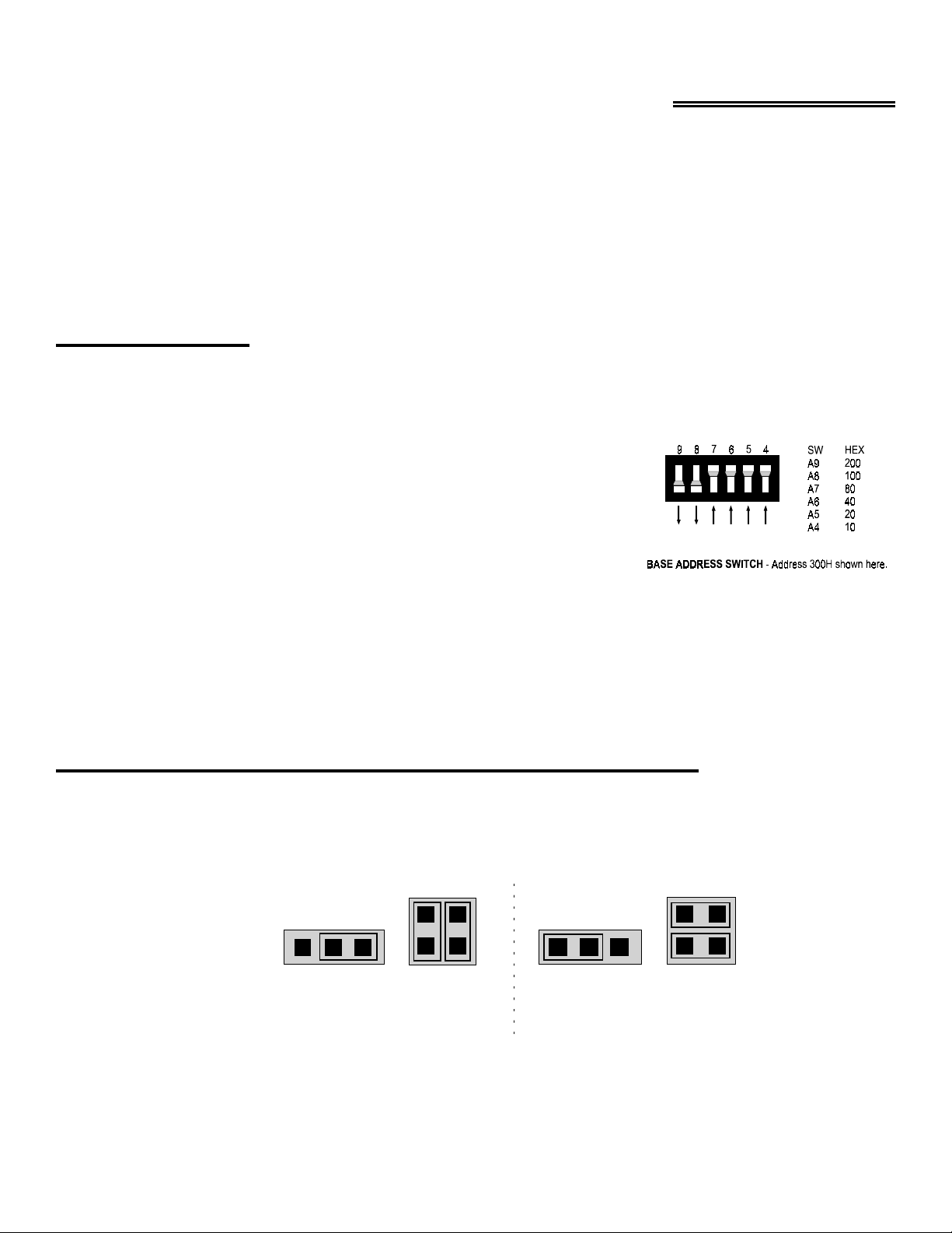
1.1 BASE ADDRESS
After a base address is chosen, a diagram of the switch setting is drawn on the PC screen. Set the switches on your base
address switch as shown on Figure 1-1. Unless there is already a board in your system which uses address 300 hex (768
decimal) then you can leave the switches as they are set at the factory.
In the diagram, the CIO-DAS16 is set for base address 300h. That means the
DAS-16 compatible section of the board is at 300h and the PIO-12 compatible
section of the board is at 310h (784 Decimal).
When the 4 addresses of the 8255 digital I/O (PIO-12) are in use, the
CIO-DAS16 occupies 20 consecutive addresses and is addressable on 32 address
boundaries. Address boundaries of 32 are 300h, 320h, 340h, 360h, etc.
Figure 1-1. Base Address Switches
Because the MetraByte DAS-16 occupies only 16 addresses, it is addressable at 300h, 310h, 320h, 330h etc. If you have
written software that assumes the DAS-16 base address is on a 16 address boundary and it is too much trouble to change
the address in software, the CIO-DAS16 can be made to occupy only 16 addresses and address on 16 address boundaries.
If you want to address the CIO-DAS16 on a 16 boundary address, such as 310h, 330h, 350h etc., you will not be able to
use the additional 24 digital I/O lines on the rear connector.
1.2 MODIFYING THE CIO-DAS16 FOR COMPATIBLE ADDRESSES
There are two jumpers on the CIO-DAS16, J3 and J4, which disable or enable the 8255. The jumpers must be configured
as a pair, according to either the (A) or (B) configuration in Figure 1-2.
J3J4
(A)CIO-DAS16 POSITION
PIO-12 is active at Base Address + 16
Board will address at 300H, 320H, 340H, etc.
Board will address at 300H, 310H, 320H, etc.
J4
(B) DAS 16 POSITION
PIO-12 is not active at any address.
J3
CIO-DAS16 PIO-12 KNOCK OUT JUMPERS - The CIO-DAS16 is shipped in the (A)
configuration. It should be left this way unless you want to use odd addressess,
such as 310H, 330H, 350H, etc. In the (B) configuration, the 24 digital lines of
the 8255 are not usable.
Figure 1-2. Odd Address Jumpers
1
Page 6

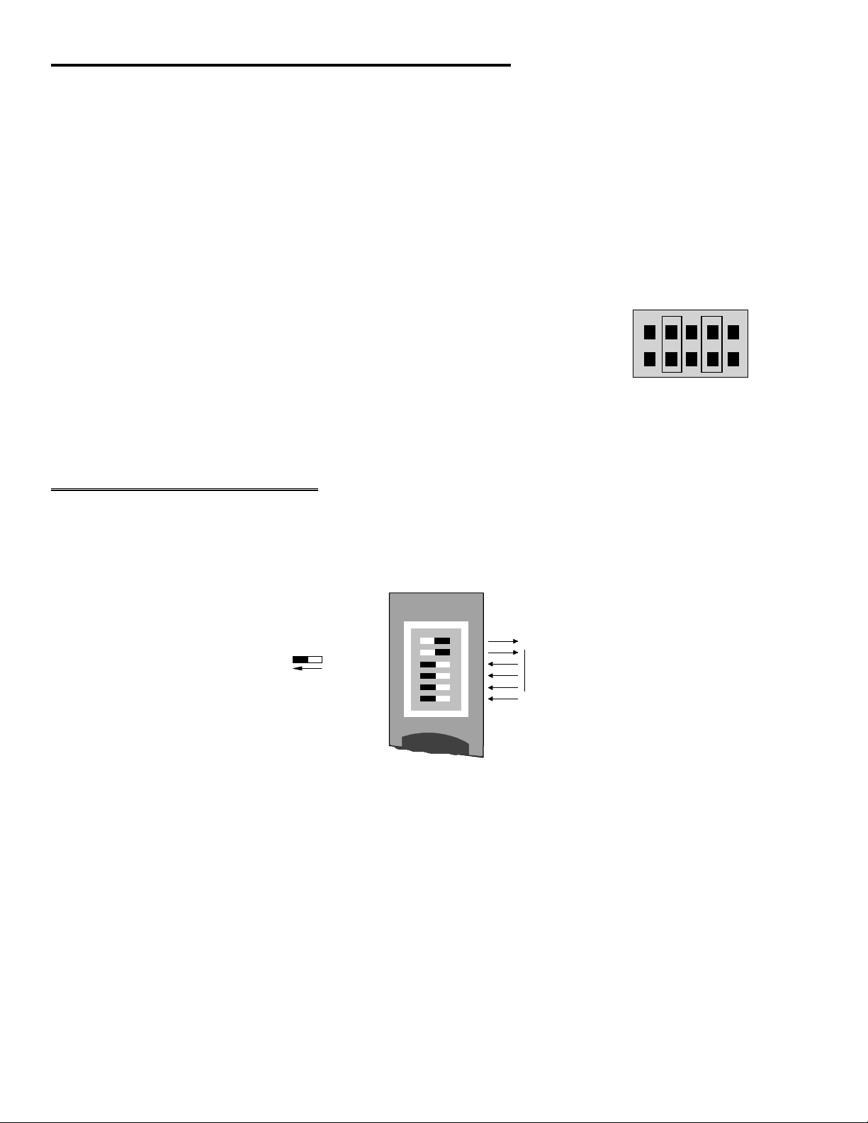
1.3 DMA LEVEL SELECT
What kind of computer are you installing the board in? If it is an old XT then there are only two DMA levels available
and level 3 is probably used by the hard disk controller in your XT computer. Set the
DMA level switch to the level 1 position (Figure 1-3).
If you have an AT or 386 type computer the hard disk controller is not at level 1 or 3
so either level may be used.
There are other boards that use DMA levels. Some network boards and some
IEEE-488 interface boards do also. If you have other boards in your computer with
DMA level switches on them, they must have a different level setting.
Figure 1-3. DMA Level Select Switch
1.4 1/10 MHZ XTAL JUMPER
The 1/10 MHz XTAL jumper selects the frequency of the source applied to the
on-board pacer. This pacer is used to pace the A/D start conversion trigger.
This jumper is on the board because the original DAS-16, designed in 1984, had
a 1 MHz crystal. When MetraByte redesigned the DAS-16 and added the faster
10 MHz crystal, a jumper was provided to maintain compatibility with older
software. The CIO-DAS16 has the jumper because the DAS-16 has the jumper
and some software needs the jumper to be in the 1 MHz position and some
software requires the 10 MHz position.
Figure 1-4. 1 or 10 MHz Xtal Jumper
The CIO-DAS16 is shipped with the jumper in the 1 MHz position.
Some older 3rd party software programs require that the jumper be in the 1 MHz position. Please refer to the software
program user's manual for guidance. Other programs, such as Labtech Notebook, have a 1 or 10 MHz choice in the
set-up menu.
1.5 8/16 CHANNEL SELECT
The analog inputs of the CIO-DAS16 may be configured as 8 differential or 16
single-ended. Using single-ended inputs means you have more separate analog
input channels available to connect signals. Using differential inputs allows up to
10 volts of common mode (ground loop) rejection and can be more noise immune.
The CIO-DAS16 comes from the factory configured for 8 differential inputs so the
8/16 switch is in the position shown here. Set it for the type and number of inputs
you desire.
Figure 1-5. 8 /16 Channel Select Switch
2
Page 7
1.6 D/A CONVERTER REFERENCE JUMPER BLOCK
There is a jumper block with 10 pins (2 rows of 5 each) located top center on the board. This block allows you to use the
on-board precision voltage reference or an external voltage to provide reference to either or both of the digital-to-analog
converters.
If you choose to use the on-board voltage reference rather than an external voltage, two D/A reference input pins, 10 and
26, on the 37-pin connector are not needed as reference inputs.
The 'S' jumper in this block is used to place a synchronizing signal on pin 26 so that the CIO-SSH16 external accessory
Simultaneous Sample & Hold board can be used.
If the on-board D/A reference is used, the jumpers are set in the I1 and I0
positions (Figure 1-6). The board is configured this way at the factory. The
SS&H output is not connected. If an external reference is desired, move the
blocks to X0 and X1. If using a CIO-SSH16 board, leave the blocks on I0
and I1 and place a block on SS&H. To avoid possible damage in the event
of a bad connection, do not install jumper S unless you intend to connect a
CIO-SSH16 board. There is a spare shorting block on one of the 'S' pins.
Figure 1-6. Ref. Volt and SS&H Jumpers
D/A 1
EXTERNAL &
INTERNAL
X I1 S I0 X
D/A 0
INTERNAL &
EXTERNAL
1.7 RANGE SWITCH SETTING
A bank of six dip switches accessible through the CIO-DAS16 connector bracket control the UNIPOLAR/BIPOLAR
analog input range (Figure 1-7).
SW #
UNIPOLAR
LEFT
NO USER GAIN
These switches control the analog input range values of all channels. You can use Table 1-1 and Figure 1-7, or use the
Cal program to determine the correct positions of switches S1 through S6 for the range you desire.
Insta
.
6
5
4
3
2
1
The factory setting of +/- 5V
BIPOLAR - SW 6 ONLY
SW 2 - 4
SELECT THE RANGE
USER GAIN SELECTED
shown.
Figure 1-7. Range Select Switches
SEE TABLE 1-1
3
Page 8

Table 1-1. Range Select Switch Positions
GAINS5S4S3S2S1
In the above table R = right and L = left.
BIPOLAR
S6=RIGHT
S6=LEFT
RESOLUTIONUNIPOLAR
4.88mV / bitN/A+/- 10V0.5LLLLL
2.44mV / bit0 to 10V+/- 5V1RLLLL
1.22mV / bit0 to 5V+/- 2.5V2RRLLL
0.488mV / bit0 to 2 V+/- 1V5RLRLL
0.244mV / bit0 to 1V+/- 0.5V10RLLRL
SEE EQUATION0.5 < USER < 20LLLLR
S6, the top switch, controls a relay that switches the range between unipolar and bipolar.
Set the switches as desired or leave them at the factory setting of +/- 5 volts.
It is not necessary to turn off the PC power or disconnect signals when changing these switch settings.
4
Page 9
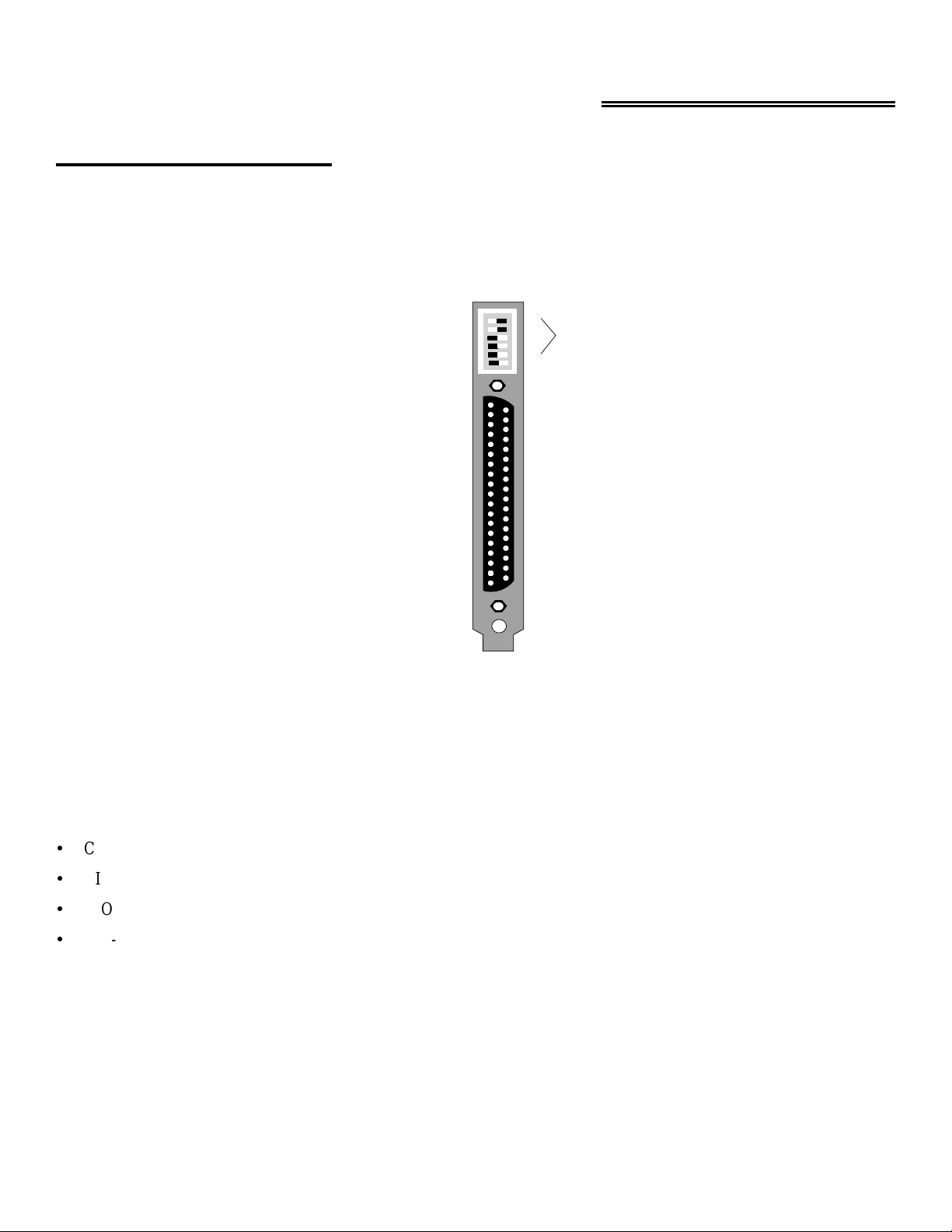
2 SIGNAL CONNECTION
2.1 CONNECTOR DIAGRAM
The CIO-DAS16 analog connector is a 37-pin, D-type connector accessible from the rear of the PC through the expansion
backplate (Figure 2-1). The signals available are identical to the DAS-16, or optionally, an additional signal, SS&H
OUT, may be accessed at pin 26.
UNIPOLAR
RR
LR
LR LL
LLRL
LL L
GAIN = 0.5 2 5 10
CH0 LOW/CH8 HIGH 18
CH1 LOW/CH9 HIGH 17
CH2 LOW/CH10 HIGH 16
CH3 LOW/CH11 HIGH 15
CH4 LOW/CH12 HIGH 14
CH5 LOW/CH13 HIGH 13
CH6 LOW/CH14 HIGH 12
CH7 LOW/CH15 HIGH 11
LLGND 19
D/A 0 REF 10
D/A 0 OUT 9
-5V REF 8
GND 7
DIG. IN 1 6
DIG. IN 3 5
DIG. OUT 1 4
DIG. OUT 3 3
CTR 0 OUT 2
+5V PC BUS 1
R
BIPOLAR
R
GAIN = 1
L
+/- 5V RANGE
L
L
USER GAIN RESISTOR
37 CH0 HIGH
36 CH1 HIGH
35 CH2 HIGH
34 CH3 HIGH
33 CH4 HIGH
32 CH5 HIGH
31 CH6 HIGH
30 CH7 HIGH
29 LLGND
28 LLGND
27 D/A 1 OUT
26 D/A 1 REF/SS&H OUT
25 DIG. IN 0/TRIGGER
24 DIG. IN 2/CTR0 GATE
23 DIG. OUT 0
22 DIG. OUT 2
21 CTR 0 CLOCK IN
20 CTR 2 OUT
CIO-DAS16 ANALOG CONNECTOR - The CIO-DAS16
analog connector can be accessed from the rear of
the computer through the expansion backplate.
Figure 2-1. Analog Connector
If frequent changes to signal connections or signal conditioning is required, please refer to the information on one of the
following:
y
CIO-TERMINAL screw terminal board
y
CIO-EXP16, 16-channel analog multiplexer
y
CIO-SSH16 16-channel simultaneous sample & hold board
y
ISO-RACK16, 16-module 5B isolation module interface rack
The CIO-DAS16 digital connector is identical to the CIO-DIO24 connector except for the −12V and +12V power signals
and interrupt input brought out on the CIO-DIO24. These are no-connect pins on the CIO-DAS16.
The digital connector is mounted at the rear of the CIO-DAS16 and will accept a 37-pin, D-type female connector such as
those on the C73FF-2, two-foot cable with connectors.
5
Page 10
A BP-37 will bring the signals to a backplate with a 37 pin male connector
g1g
mounted in it.
A standard C37FF-2 may be run alongside the analog connector through the
gap in the expansion slot backplate, or may be connected to the BP-37.
2.2 ANALOG INPUTS
Analog inputs to the CIO-DAS16 can be connected in three different
configurations:
y
Single-Ended
y
Floating Differential
y
Differential.
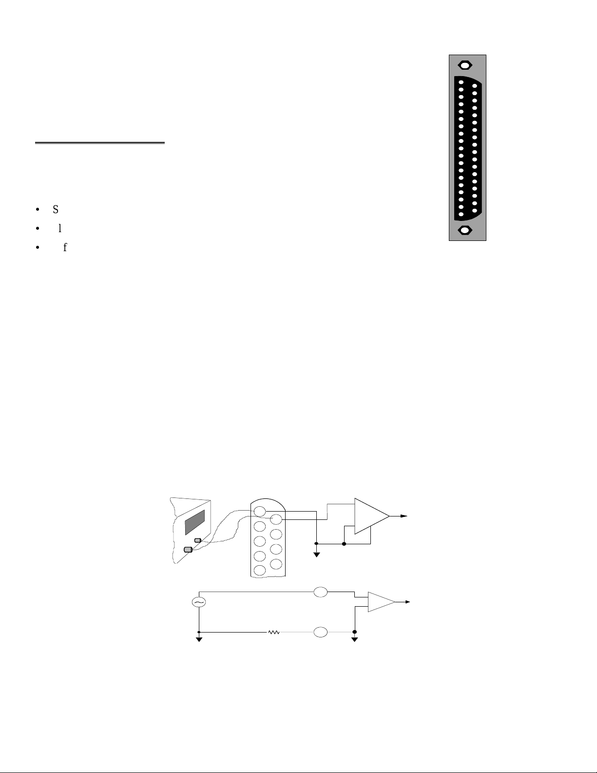
WARNING - PLEASE READ
Measure the voltage between the ground signal at the signal source and the PC. Using a voltmeter, place
the red probe on the PC ground and the black probe on the signal ground. If there is more than 10 volts
(AC or DC), do not connect the CIO-DAS16 to this signal source because you will not be able to make
any reading. If more than 30 volts, DO NOT connect this signal to the CIO-DAS16 because it will
damage the board and possibly the computer. Voltages over 24V can be hazardous. Use great care
when measuring voltages.
19
GND
+5V
GND
NC
GND
NC
GND
NC
GND
PORT B 0
PORT B 1
PORT B 2
PORT B 3
PORT B 4
PORT B 5
PORT B 6
PORT B 7
NC
NC
18
17
16
15
14
13
12
11
10
9
8
7
6
5
4
3
2
1
37
36
35
34
33
32
31
30
29
28
27
26
25
24
23
22
21
20
PORT A 0
PORT A 1
PORT A 2
PORT A 3
PORT A 4
PORT A 5
PORT A 6
PORT A 7
PORT C 0
PORT C 1
PORT C 2
PORT C 3
PORT C 4
PORT C 5
PORT C 6
PORT C 7
GND
+5V
CIO-DAS16 DIGITAL CONNECTOR - The connector
is mounted at the rear of the CIO-DAS 16.
Figure 2-2. Digital Connector
SINGLE-ENDED
A single-ended input has two wires connected to the CIO-DAS16; a channel high (CH# HI) and a Low Level Ground
(LLGND). The LLGND signal must be the same ground the PC is on. The CH# HI is the voltage signal source.
DIFFERENTIAL
Vs+Vcm
AMP
+
-
+
-
2
TO A/D
GND
S
I
G
N
A
L
V+
Vs
37
36
35
34
LL GND
CH 0 HI
HI
G
19
18
17
16
15
SIGNAL ENDED INPUT - A channel high (CH 0 HI) and a low level ground
(LLGND) are connected to the CIO-DAS16.
Figure 2-3. Single-Ended Input Configuration
6
Page 11
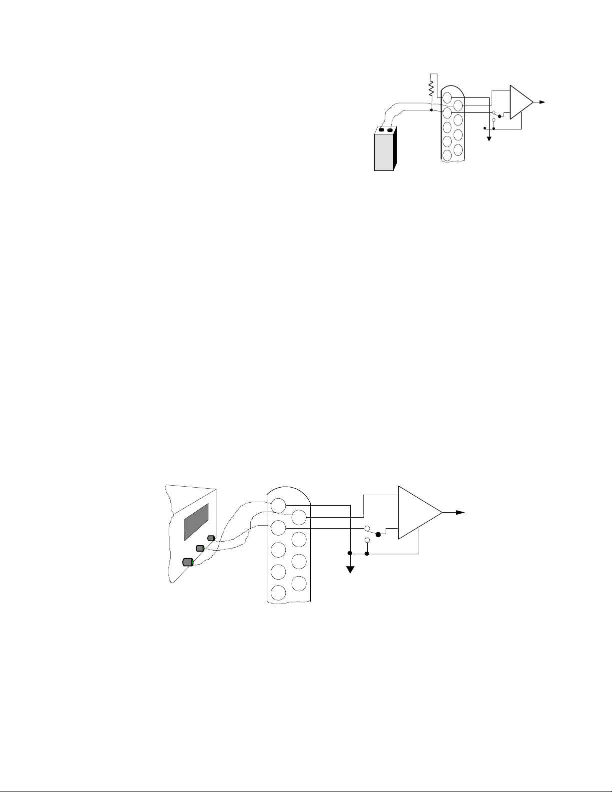
FLOATING DIFFERENTIAL
A floating differential input is two wires from the signal source and a
10K ground reference resistor installed at the CIO-DAS16 input. The
two signals from the signal source are Signal High (CH# HI) and
Signal Low (CH# LO) (Figure 2-4).
The reference resistor is connected between the CIO-DAS16 CH# LO
and LLGND pins.
A floating differential hookup is useful when the signal source is
floating with respect to ground, such as a battery, 4-20 mA transmitter
or the lead lengths are long or subject to EMI.
The floating differential input will reject up to 10V of EMI.
WARNING!
Verify that the signal source is floating. Check it with a voltmeter before risking the CIO-DAS16 and PC!
DIFFERENTIAL
10K OHM
-
+
BATTERY
CIO-DAS16 FLOATING DIFFERENTIAL - The two
signals from the signal source are Signal High
(CH 0 HI) and Signal Low (CH 0 LO).
LL GND
19
CH 0 HI
37
CH 0 LO
18
36
17
35
16
34
15
AMP
+
8
16
TO A/D
-
Figure 2-4. Floating Differential Input
DIFFERENTIAL
A differential signal has three wires from the signal source. The signals are Signal High (CH# HI), Signal Low (CH# LO)
and Signal Ground (LLGND) (Figure 2-5).
A differential connection allows you to connect the CIO-DAS16 to a signal source with a ground that is different from
the PC ground, but less than 10V difference, and still make a true measurement of the signal between CH# HI and CH#
LO.
DIFFERENTIAL
AMP
37
36
35
34
LL GND
CH 0 HI
CH 0 LO
8
19
V-
V+
18
17
GND
16
15
CIO-DAS16 DIFFERENTIAL - The signals are Signal High (CH 0 HI), Signal Low
(CH 0 LO), and Signal Ground (LLGND).
+
TO A/D
-
16
Figure 2-5. Differential Input
EXAMPLE:
A laboratory instrument with its own wall plug. There are sometimes voltages in wall GND between outlets.
7
Page 12

2.3 ANALOG OUTPUTS
Analog outputs are voltage outputs which can be connected to any device which will record, display or be controlled by a
voltage.
The CIO-DAS16 analog outputs are 4 quadrant multiplying DACs. This means that they accept an input voltage reference
and provide an output voltage which is inverse to the reference voltage and proportional to the digital value in the output
register.
For example, the supplied reference of -5V provides a +5V output when the value in the output register is 4095 (full scale
at 12 bits of resolution). It provides a value of 2.5V when the value in the output register is 2048 (Figure 2-6).
D/A REFERENCE BLOCK
ISIX
X
D/A 0
ON BOARD -5 REF
V REF
V OUT =
V OUT
-1(V REF) * DATA
CIO-DAS16 37 PIN CONNECTOR
19
LLGND
18
D/A 0
-5 REF
10
9
8
D/A 0 REF
4096
37
28
LLGND
27
D/A 1
26
D/A 1 REF
GROUND
VOLTS OUT
CIO-DAS16 D/A CONVERTER SIGNAL CONNECTION - Jumper blocks for
internal Vref shown installed. The on-board -5V reference is internally
jumped. Both DACs will have a range of 0 to 5 volts. This is the factory
Figure 2-6. Analog Output Configuration
2.4 DIGITAL OUTPUTS & INPUTS
All the digital outputs and inputs on the CIO-DAS16 are TTL level. TTL is an electronics industry term, short for
Transistor Transistor Logic, that describes a standard for digital signals which are either at 0V or 5V (nominal). The
binary logic inside the PC is all TTL or LSTTL (Low power Schotky TTL).
8
Page 13

3 ANALOG CONNECTIONS
3.1 ANALOG INPUTS
Although complete coverage of this topic is well beyond the scope of this manual, the following section provides some
explanations and helpful hints regarding these analog input connections. This section is intended to help you achieve the
optimum performance from your CIO-DAS16/F series board.
You should have a basic understanding of Single-Ended/Differential inputs and system grounding/isolation. If you are
already comfortable with these concepts you may wish to skip to the next section (on wiring configurations).
3.2 SINGLE-ENDED AND DIFFERENTIAL INPUTS
The CIO-DAS16/F provides either eight differential or 16 single-ended input channels. The concepts of single-ended and
differential inputs are discussed in the following section.
Single-Ended Inputs
A single-ended input measures the voltage between the input signal and ground. In this case, in single-ended mode the
CIO-DAS16/F measures the voltage between the input channel and LLGND. The single-ended input configuration
requires only one physical connection (wire) per channel and allows the CIO-DAS16/F to monitor more channels than the
(2-wire) differential configuration using the same connector and onboard multiplexor. However, since the CIO-DAS16/F
is measuring the input voltage relative to its own low level ground, single-ended inputs are more susceptible to both EMI
(Electro Magnetic Interference) and any ground noise at the signal source. Figure 3-1 shows the single-ended input
configuration.
Figure 3-1. Single-Ended Input Configuration
9
Page 14

Differential Inputs
Differential inputs measure the voltage between two distinct input signals. Within a certain range (referred to as the
common mode range), the measurement is almost independent of signal source to CIO-DAS16/F ground variations. A
differential input is also much more immune to EMI than a single-ended one. Most EMI noise induced in one lead is also
induced in the other, the input only measures the difference between the two leads, and the EMI common to both is
ignored. This effect is a major reason there is twisted pair wire as the twisting assures that both wires are subject to
virtually identical external influence. Figure 3-2 below shows a typical differential input configuration.
Figure 3-2. Differential Input Configuration
10
Page 15

Before moving on to the discussion of grounding and isolation, it is important to explain the concepts of common mode,
and common mode range (CM Range). Common mode voltage is depicted in Figure 3-2 as Vcm. Though differential
inputs measure the voltage between two signals, without (almost) respect to the either signal’s voltages relative to
ground, there is a limit to how far away from ground either signal can go. Though the CIO-DAS16/F has differential
inputs, it will not measure the difference between 100V and 101V as 1 Volt (in fact the 100V would destroy the board!).
This limitation or common mode range is depicted graphically in Figure 3-3. The CIO-DAS16/F common mode range is
+/- 10 Volts. Even in differential mode, no input signal can be measured if it is more than 10V from the board’s low level
ground (LLGND).
+13V
+12V
+11V
+10V
+9V
+8V
+7V
+6V
+5V
+4V
+3V
+2V
+1V
-1V
-2V
-3V
-4V
-5V
-6V
-7V
-8V
-9V
-10V
-11V
-12V
-13V
System Grounds and Isolation
Gray area represents common m ode range
Both V+ and V- must always re ma in w it h in
the common m ode range re la tiv e to L L Gn d
With Vcm= +5VDC,
+Vs must be less than +5V, or the common mod e range w ill be e x c eeded (>+10V)
Vcm
Vcm (Common M ode Voltage) = +5 Volts
Figure 3-3. Common Mode Range Diagram
There are three scenarios possible when connecting your signal source to your CIO-DAS16/F board.
1. The CIO-DAS16/F and the signal source may have the same (or common) ground. This signal source may be
connected directly to the CIO-DAS16/F.
2. The CIO-DAS16/F and the signal source may have an offset voltage between their grounds (AC and/or DC). This
offset it commonly referred to a common mode voltage. Depending on the magnitude of this voltage, it may or may not
be possible to connect the CIO-DAS16/F directly to your signal source. We will discuss this topic further in a later
section.
3. The CIO-DAS16/F and the signal source may already have isolated grounds. This signal source may be connected
directly to the CIO-DAS16/F.
Which system do you have?
1
Perform the following test: Using a battery powered voltmeter
, measure the voltage (AC and DC) between the ground
signal at your signal source and at your PC. Place one voltmeter probe on the PC ground and the other on the signal
source ground. Measure both the AC and DC Voltages.
1
If you do not have access to a voltmeter, skip the experiment and take a look at the following three sections. You may be able to identify your system type from the
descriptions provided.
11
Page 16

If both AC and DC readings are 0.00 volts, you may have a system with common grounds. However, since voltmeters
will average out high frequency signals, there is no guarantee. Please refer to the section below titled Common Grounds.
If you measure reasonably stable AC and DC voltages, your system has an offset voltage between the grounds category.
This offset is referred to as a Common Mode Voltage. Please be careful to read the following warning and then proceed
to the section describing Common Mode systems.
WARNING
If either the AC or DC voltage is greater than 10 volts, do not connect the CIO-DAS16/F to this signal
source. You are beyond the boards usable common mode range and will need to either adjust your
grounding system or add special Isolation signal conditioning to take useful measurements. A ground
offset voltage of more than 30 volts will likely damage the CIO-DAS16/F board and possibly your
computer. Note that an offset voltage much greater than 24 volts will not only damage your electronics,
but it may also be hazardous to your health. In this case you will need to either reconfigure your system
to reduce the ground differentials, or install special electrical isolation signal conditioning.
If you cannot obtain a reasonably stable DC voltage measurement between the grounds, or the voltage drifts around
considerably, the two grounds are most likely isolated. The easiest way to check for isolation is to change your voltmeter
to it’s ohm scale and measure the resistance between the two grounds. It is recommended that you turn both systems off
prior to taking this resistance measurement. If the measured resistance is more than 100 Kohm, it’s a fairly safe bet that
your system has electrically isolated grounds.
Systems with Common Grounds
In the simplest (but perhaps least likely) case, your signal source will have the same ground as the CIO-DAS16/F. This
would typically occur when providing power or excitation to your signal source directly from the CIO-DAS16/F. There
may be other common ground configurations, but it is important to note that any voltage between the CIO-DAS16/F
ground and your signal ground is a potential error voltage if you set up your system based on a common ground
assumption.
As a safe rule of thumb, if your signal source or sensor is not connected directly to an LLGND pin on your
CIO-DAS16/F, it’s best to assume that you do not have a common ground even if your voltmeter measured 0.0 Volts.
Configure your system as if there is ground offset voltage between the source and the CIO-DAS16/F. This is especially
true if you are using either the CIO-DAS1402/16 or the CIO-DAS1402/12 at high gains, since ground potentials in the
sub millivolt range will be large enough to cause A/D errors, yet will not likely be measured by your handheld voltmeter.
Systems with Common Mode (ground offset) Voltages
The most frequently encountered grounding scenario involves grounds that are somehow connected, but have AC and/or
DC offset voltages between the CIO-DAS16/F and signal source grounds. This offset voltage my be AC, DC or both and
may be caused by a wide array of phenomena including EMI pickup, resistive voltage drops in ground wiring and
connections, etc. Ground offset voltage is a more appropriate term to describe this type of system, but since our goal is to
keep things simple, and help you make appropriate connections, we’ll use the phrase Common Mode.
Small Common Mode Voltages
If the voltage between the signal source ground and CIO-DAS16/F ground is small, the combination of the ground
voltage and input signal will not exceed the CIO-DAS800’s +/-10V common mode range, (i.e. the voltage between
grounds, added to the maximum input voltage, stays within +/-10V), This input is compatible with the CIO-DAS16/F and
the system may be connected without additional signal conditioning. Fortunately, most systems will fall in this category
and have a small voltage differential between grounds.
Large Common Mode Voltages
If the ground differential is large enough, the CIO-DAS800’s +/- 10V common mode range will be exceeded (i.e. the
voltage between CIO-DAS16/F and signal source grounds, added to the maximum input voltage you’re trying to measure
exceeds +/-10V). In this case the CIO-DAS16/F cannot be directly connected to the signal source. You will need to
12
Page 17

change your system grounding configuration or add isolation signal conditioning. (Please look at our ISO-RACK and
ISO-5B-series products to add electrical isolation, or give our technical support group a call to discuss other options).
NOTE
Relying on the earth prong of a 120VAC for signal ground connections is not advised.. Different ground
plugs may have large and potentially even dangerous voltage differentials. Remember that the ground
pins on 120VAC outlets on different sides of the room may only be connected in the basement. This
leaves the possibility that the “ground” pins may have a significant voltage differential (especially if the
two 120 VAC outlets happen to be on different phases!)
CIO-DAS16/F and Signal Source Having Isolated Grounds
Some signal sources will already be electrically isolated from the CIO-DAS16/F. The diagram below shows a typical
isolated ground system. These signal sources are often battery powered, or are fairly expensive pieces of equipment
(since isolation is not an inexpensive proposition), isolated ground systems provide excellent performance, but require
some extra effort during connections to assure optimum performance is obtained. Please refer to the following sections
for further details
3.3 WIRING CONFIGURATIONS
Combining all the grounding and input type possibilities provides us with the following potential connection
configurations. The combinations along with our recommendations on usage are shown in Table 3-1 below.
GROUND
CATEGORY
Common Mode
Voltage < +/-10V
Common Mode
Voltage < +/-10V
Common Mode
Voltage > +/- 10V
Common Mode
Voltage > +/-10V
Already Isolated
Grounds
Table 3-1. Input Type Recommendations
INPUT
OUR VIEW
CONFIGURATION
RecommendedSingle-Ended InputsCommon Ground
AcceptableDifferential InputsCommon Ground
Not RecommendedSingle-Ended Inputs
RecommendedDifferential Inputs
Unacceptable without
Single-Ended Inputs
adding Isolation
Unacceptable without
Differential Inputs
adding Isolation
AcceptableSingle-ended InputsAlready Isolated Grounds
RecommendedDifferential Inputs
The following sections depicts recommended input wiring schemes for each of the eight possible input
configuration/grounding combinations.
13
Page 18

3.3.1 Common Ground / Single-Ended Inputs
g
g
g
Single-ended is the recommended configuration for common ground connections. However, if some of your inputs are
common ground and some are not, we recommend you use the differential mode. There is no performance penalty (other
than loss of channels) for using a differential input to measure a common ground signal source. However the reverse is
not true. Figure 3-4 below shows a recommended connection diagram for a common ground / single-ended input system
NOTE: For simplicity, the input multiplexer is not shown in the following diagrams.
Signal
S our c e w ith
C om m on Gn d
Optional wire
since signal source
and A/D board share
common ground
I/O
Connector
CH IN
LL GND
Signal source and A/D board
sharin
common ground connected
to s in
le- en d e d in p u t.
+
Inp u t
Amp
-
A/D Board
To A / D
.
y
Figure 3-4.
Single-Ended
Input
3.3.2 Common Ground / Differential Inputs
The use of differential inputs to monitor a signal source with a common ground is a acceptable configuration though it
requires more wiring and offers fewer channels than selecting a single-ended configuration. Figure 3-5 shows the
recommended connections in this configuration.
Signal
So ur ce w ith
Co mm o n G n d
Optiona l w ire
since signal source
and A/D board sha re
common ground
Figure 3-5. Common Ground - Differential Input
Required conn ection
of LL GND to CH Low
I/O
Connector
CH High
CH Low
LL GND
Signal source and A/D board
sharin
com m on ground connected
to differential input.
+
Input
Amp
-
A/D Board
To A /D
14
Page 19

3.3.3 Common Mode Voltage < +/-10V/Single-Ended Inputs
g
g
g
g
g
g
g
g
g
This is not a recommended configuration. In fact, the phrase common mode has no meaning in a single-ended system and
this case would be better described as a system with offset grounds. Anyway, you are welcome to try this configuration,
no system damage should occur and depending on the overall accuracy you require, you may receive acceptable results.
Signal Source
w ith Com m o n
Mo d e Vol ta g e
The voltage differential
between these grounds,
added to the maximum
input signal must stay
within +/-10 V
Signal source and A/D board
with common m ode volta
connected to a differential input.
GND
I/O
Connector
CH Hi
CH Low
LL GND
h
+
Inp ut
Amp
-
A/D Board
To A / D
e
Figure 3-6.
Common Mode Voltage < +/-10V/Single-Ended Inputs
3.3.4 Common Mode Voltage < +/-10V/Differential Inputs
Systems with varying ground potentials should always be monitored in the differential mode. Care is required to assure
that the sum of the input signal and the ground differential (referred to as the common mode voltage) does not exceed the
common mode range of the A/D board (+/-10V on the CIO-DAS16/F). Figure 3-7 shows recommended connections in
this configuration.
Iso la tio n
Barrier
arge common
L
mode voltage
between signal
source & A/D board
When the voltage difference
between si
A/D board
enou
common mode ran
exceeded, isolated si
conditionin
System with a Large Common Mode Voltage,
GND
nal source and
round is large
h so the A/D board’s
e is
nal
must be added.
Connected to a Sin
CH IN
LL GND
I/O
Conn ector
le-Ended Input
+
Input
Amp
-
A/D Board
To A /D
Figure 3-7. Common Mode Voltage < +/-10V/Differential Inputs
15
Page 20

3.3.5 Common Mode Voltage > +/-10V
g
g
g
g
g
g
g
The CIO-DAS16/F will not directly monitor signals with common mode voltages greater than +/-10V. You will either
need to alter the system ground configuration to reduce the overall common mode voltage, or add isolated signal
conditioning between the source and your board (Figure 3-8).
Isolation
Barrier
arge comm on
L
mode voltage
between signa l
source & A/D bo a rd
GND
10 K
CH Hi
CH Low
LL GND
h
+
Inpu t
Amp
To A / D
-
When the voltage difference
nal source and
between si
round is large
A/D board
enou
h so the A/D board’s
comm on m ode ran
exceeded, isolated si
conditionin
e is
nal
must be added.
10K is a recommended value. You may short LL GND to CH Low
instead, but this will reduce your system’s noise immunity.
I/O
Connector
A/D Board
System with a Large Com m on M ode Voltage,
Connected to a Differential Input
Figure 3-8. Common Mode Voltage > +/-10V - Differential Input
3.3.6 Isolated Grounds / Single-Ended Inputs
Single-ended inputs can be used to monitor isolated inputs, though the use of the differential mode will increase you
system’s noise immunity. Figure 3-9 shows the recommended connections is this configuration.
Isolated
signal
s o urc e
CH IN
LL GND
I/O
Connector
+
-
Inpu t
Amp
To A /D
A/D Board
Iso lat e d S ignal Source
Connected to a Single-Ended Input
Figure 3-9. Isolated Grounds / Single-Ended Inputs
16
Page 21

3.3.7 Isolated Grounds / Differential Inputs
g
Optimum performance with isolated signal sources is assured with the use of the differential input setting. Figure 3-10 below shows the
recommend connections is this configuration..
Signal Source
an d A/D Bo a rd
A lread y I s o la te d .
GND
10 K
CH High
CH Low
LL GND
+
-
Input
Amp
To A /D
These
rounds are
electrically isolated.
Figure 3-10. Isolated Grounds/Differential Inputs
I/O
Connector
10K is a recommended value. You m ay short LL GND to CH Low
instead, but this will reduce your system’s noise imm unity.
Already isolated signal source
and A/D board connected to
a differential input.
A/D Board
17
Page 22

4 CIO-DAS16 CONTROL & DATA REGISTERS
4.1 INTRODUCTION
The CIO-DAS16 is controlled and monitored by writing to and reading from 20 consecutive 8-bit I/O addresses
(registers). The first address, or BASE ADDRESS, is determined by setting a bank of switches on the board.
Register manipulation is best done by experienced programmers since most of the CIO-DAS16 functions are
implemented in easy-to-use Universal Library™ routines.
The register descriptions all follow the format:
01234567
A/D11A/D10A/D9
LSB
The numbers along the top row are the bit positions within the 8-bit byte and the numbers and symbols in the bottom row
are the functions associated with that bit.
To write to or read from a register in decimal or HEX, the following weights apply (Table 4-1):
CH1CH2CH4CH8A/D12
Table 4-1. Register Bit Weights
HEX VALUEDECIMAL VALUEBIT POSITION
110
221
442
883
10164
20325
40646
801287
To write control or data to a register, the individual bits must be set to 0 or 1 then combined to form a byte.
The method of programming required to set/read bits from bytes is beyond the scope of this manual.
In summary form, the registers and their function are listed on Table 4-2. Within each register are eight bits which may
constitute a byte of data or eight individual bit read/write functions.
18
Page 23

Table 4-2. Register Summary
WRITE FUNCTIONREAD FUNCTIONADDRESS
Start A/D FunctionA/D Bits 9 - 12 (LSB) & Channel #BASE
NoneA/D Bits 1 (MSB) - 8BASE + 1
Channel MUX SetChannel MUX ReadBASE + 2
Digital 4 Bit OutputDigital 4 Bit InputBASE + 3
D/A 0 Bits 9-12 (LSB)NoneBASE + 4
D/A 0 Bits 1(MSB)-8NoneBASE + 5
D/A 1 Bits 9-12 (LSB)NoneBASE + 6
D/A 1 Bits 1(MSB) - 8NoneBASE + 7
Interrupt ResetStatus EOC, UNI/BIP etc.BASE + 8
Set DMA, INT etcDMA, Interrupt & Trigger ControlBASE + 9
NonePacer clock control register.BASE + 10
Reserved for future use.BASE + 11
Counter 0 DataCounter 0 DataBASE + 12
CTR 1 Data - A/D Pacer CTR 1 Data - A/D Pacer ClockBASE + 13
CTR 2 Data - A/D Pacer CTR 2 Data - A/D Pacer ClockBASE + 14
Pacer Clock Control (8254)None. No read back on 8254BASE + 15
Port A OutputPort A Input of 8255BASE + 16
Port B OutputPort B Input BASE + 17
Port C OutputPort C InputBASE + 18
Configure 8255None - No read back on 8255BASE + 19
4.2 A/D DATA & CHANNEL REGISTERS
BASE ADDRESS
01234567
A/D11A/D10A/D9
LSB
A read/write register.
READ:
On read, it contains two types of data. The least significant four digits of the analog input data and the channel number
which the current data was taken from.
These four bits of analog input data must be combined with the eight bits of analog input data in BASE + 1, forming a
complete 12-bit number. The data is in the format 0 = minus full scale. 4095 = +FS.
The channel number is binary-coded. The weights are shown in Table 4-1. For example, if the current channel were five,
then bits CH4 and CH1 would be high and CH8 and CH2 would be low.
WRITE:
CH1CH2CH4CH8A/D12
Writing any data to the register causes an immediate A/D conversion.
19
Page 24

BASE ADDRESS +1
01234567
A/D8A/D7A/D6A/D5A/D4A/D3A/D 2A/D1
MSB
A Read-only register.
On read, the most significant A/D byte is read.
4.3 CHANNEL MUX SCAN LIMITS REGISTER
BASE ADDRESS +2
01234567
CH L1CH L2CH L4CH L8CH H1CH H2CH H4CH H8
A read and write register.
READ:
The current channel scan limits are read as one byte. The high channel number scan limit is in the most significant four
bits. The low channel scan limit is in the least significant four bits.
WRITE:
The channel scan limits desired are written as one byte. The high channel number scan limit is in the most significant
four bits. The low channel scan limit is in the least significant four bits.
That is one way of looking at this register, and probably the most sensible way. In fact, the bits 3-0 contain the starting
channel number and bits 7-4 contain the ending channel number. If you wanted to scan channels 1, 2, 3 in that order, you
could do so by placing the 3 in bits 7-4 and the 1 in bits 3-0.
NOTE
Every write to this register sets the current A/D channel MUX setting to the number in bits 0-3. See
BASE + 8.
4.4 FOUR-BIT DIGITAL I/O REGISTERS
BASE ADDRESS +3
01234567
D12,
D130001
CTR 0
GATE
DI0,
TRIGDI1
20
Page 25

READ:
The signals present at the inputs are read as one byte, the digital input data being contained in the four least significant
bits. The pins 25 (digital input 0) and 24 (digital input 2) digital inputs have two functions each.
The TRIG function of digital input 0 may be used to hold off the first sample of an A/D set by holding it low (0V) until
you are ready to take samples, which are then paced by the 82C54. It can also be used as the source of an external start
conversion pulse, synchronizing A/D conversions to some external event.
BASE ADDRESS +3
01234567
DO0DO1DO2DO3XXXX
WRITE:
The upper four bits are ignored. The lower four bits are latched TTL outputs. Once written, the state of the inputs cannot
be read back because a read back would read the separate digital input lines (see above).
NOTE
The digital lines 0 to 4, pins 3, 4, 5, 6, 22, 23, 24, and 25 of the analog connector should not be used as
ON/OFF Digital I/O. Read on.
The digital inputs have multiple functions as described above. The digital outputs are also used by the CIO-EXP family
of multiplexer expansion boards. The original DAS-16 design had insufficient number of digital I/O, so we added a
PIO-12 compatible 24-line 8255 to the design. We suggest that you use these lines for ON/OFF digital functions, keeping
the 4-bit ports on the analog connector free.
4.5 D/A REGISTERS
D/A 0 REGISTERS
BASE ADDRESS +4
01234567
D/A11D/A10D/A9
LSB
BASE ADDRESS+5
XXXXD/A12
01234567
D/A8D/A7D/A6D/A5D/A4D/A3D/A2D/A1
21
Page 26

D/A 1 REGISTERS
BASE ADDRESS +6
01234567
XXXXD/A12D/A11D/A10D/A9
BASE ADDRESS +7
01234567
D/A8D/A7D/A6D/A5D/A4D/A3D/A2D/A1
WRITE ONLY:
Each 12-bit D/A output line has two registers. The first contains the four least significant bits of the data and four bits
that don't matter. The second register contains the eight most significant bits of the data.
The D/A will be updated when the eight most significant bits (upper register) are written. In this way, the lower four bits
can be written with no effect on the D/A output until the remainder of the data is written to the upper eight bits.
4.6 STATUS REGISTER
BASE ADDRESS + 8
01234567
CH1CH2CH4CH8INTMUXU/BEOC
A read mostly, one-function-write register.
READ:
EOC = 1, the A/D converter is busy. EOC = 0, it is free.
U/B = 1, the amplifier is in Unipolar mode. U/B = 0, is bipolar.
MUX = 1, Channels are configured 16 single ended. MUX = 0, 8 differential.
INT = 1, an external pulse has been received. INT = 0, the flip-flop is ready to receive a pulse..
There is a flip-flop on the TRIGGER input (pin 25) which will latch a pulse as short as 200 ns. After being triggered, this
flip-flop must be reset by a write to this register. Your interrupt service routine must do this before another interrupt
trigger can be received.
CH8, CH4, CH2 and CH1 make up a binary number between 0 and 15 indicating the channel number that the MUX is
currently set to. It is valid only when EOC = 0. The channel MUX increments shortly after EOC = 1 so may be in a state
of transition when EOC = 1. The binary weight of each bit is shown in Table 4-1.
WRITE:
A write of any data to this register resets the flip-flop on the pin 25 input and sets the INT bit to 0.
22
Page 27

4.7 DMA, INTERRUPT & TRIGGER CONTROL
BASE ADDRESS + 9
01234567
TS0TS1DMADon’t CareIR1IR2IR4INTE
A read and write register.
READ OR WRITE:
INTE = 1, Interrupts are enabled. An interrupt generated will be placed on the PC bus interrupt level selected by IR4,
IR2, and IR1. When INTE = 0, interrupts are disabled.
IR4, IR2, and IR1 are bits in a binary number between 0 and 7 which map interrupts onto the PC bus interrupt levels 2 to
7. Interrupts 0 and 1 can not be asserted by the CIO-DAS16.
When DMA = 1, DMA transfers are enabled. When DMA = 0, DMA transfers are disabled. Note that a DMA request
can be asserted only on the DMA request level selected by the DMA switch on the board. Before this bit is set to 1, the
PC's 8237 (or appropriate) DMA controller chip must be set up.
TS1 & TS0 control the source of the A/D start conversion trigger according to Table 4-3 below.
Table 4-3. Start Conversion Trigger Source - Control Bit Coding
TS0TS1
Action
Software triggered A/D onlyX0
Start on rising TRIGGER (Digital input 0, Pin 25)01
Start on Pacer Clock Pulse (CTR 2 OUT, no external access)11
4.8 PACER CLOCK CONTROL REGISTER
BASE ADDRESS +10
01234567
TRIG0CTR0XXXXXX
Write only
When CTR0 = 1, an on-board 100 KHz clock signal i s ANDed with the COUNTER 0 CLOCK INPUT (pin 21) . A high
on pin 21 will allow pulses from the on-board source into the 8254 Counter 0 input.
When CTR0 = 0, the input to 82C54 Counter 0 is entirely dependent on pulses at pin 21, COUNTER 0 CLOCK INPUT.
TRIG0 = 1. The TRIGGER input at pin 25 is ANDed with TRIG0 which controls gating of the on-board pacer clock
(82C54). When TRIG0 = 1, the on-board pacer clock can be gated off (disabled) by pulling pin 25 low. The input at pin
25 is pulled up and will always be high unless pulled low externally.
23
Page 28

When TRIG0 = 0, the external trigger at pin 25 has no effect on the GATEs of counter 1 and 2.
See Figure 4-1 for a block diagram of the Pacer Clock logic.
Figure 4-1. Pacer Clock and Control Logic
+5V
10K
COUNTER 0
COUNTER 1
COUNTER 2
A/D PACER
OUT
OUT
OUT
24
CTR 0 GATE
CTR 0 CLOCK IN
21
2
CTR 0 OUT
20
CTR 2 OUT
TRIGGER
25
CONTROL REGISTER
BASE + 10
TRIG0
CTR0
10 MHz
1 /10
1 /10
10 MHz
1MHz
+5V
10K
GATE
GATE
GATE
+5V
10K
4.9 BASE + 11 - RESERVED REGISTER
BASE ADDRESS + 11
This address is reserved for use as a programmable gain register in other DAS16 family boards.
4.10 PACER CLOCK DATA & CONTROL REGISTERS
8254 COUNTER 0 DATA
BASE ADDRESS +12
8254 COUNTER 1 DATA
BASE ADDRESS +13
24
01234567
D0D1D2D3D4D5D6D7
01234567
D0D1D2D3D4D5D6D7
Page 29

82C54 COUNTER 2 DATA
BASE ADDRESS +14
01234567
D0D1D2D3D4D5D6D7
The three 82C54 counter/timer data registers may be written to and read from. Because each counter can count to
65,535, loading or reading the counter data must be a multi-step process. The operation of the 82C54 is explained in the
Intel 82C54 data sheet.
82C54 COUNTER CONTROL
BASE ADDRESS +15
01234567
D0D1D2D3D4D5D6D7
This register controls the operation and loading/reading of the counters. The configuration of the 82C54 codes which
control the 82C54 chip is explained in the Intel 82C54 data sheet.
4.11 24-LINE DIGITAL I/O REGISTERS
PORT A DATA
BASE ADDRESS +16
01234567
A0A1A2A3A4A5A6A7
PORT B DATA
BASE ADDRESS +17
01234567
B0B1B2B3B4B5B6B7
Ports A and B may be programmed as input or output. Each is written to and read from in bytes, although for control and
monitoring purposes the individual bits are used.
Bit set/reset and bit read functions require that unwanted bits be masked out of reads and ORed into writes.
PORT C DATA
BASE ADDRESS +18
01234567
C0C1C2C3C4C5C6C7
CL0CL1CL2CL3CH0CH1CH2CH3
25
Page 30

Port C may be used as one 8-bit port of either input or output, or it may be split into two 4-bit ports which can be
independently input or output. The notation for the upper 4-bit port is CH3 to CH0, and for the lower, CL3 to CL0.
Although it may be split, every read and write to port C carries eight bits of data so unwanted information must be
ANDed out of reads, and writes must be ORed with the current status of the other port.
OUTPUT PORTS:
In 8255 mode 0 configuration, ports configured for output, hold the output data written to them. The output byte may be
read back by reading a port configured for output.
INPUT PORTS:
In 8255 mode 0 configuration, ports configured for input, read the state of the input lines at the moment, transitions are
not latched.
8255 CONTROL REGISTER
BASE ADDRESS +19
01234567
CLBM1CHAM2M3MS
Group BGroup A
The 8255 can be programmed to operate in Input/Output (mode 0), Strobed Input/Output (mode 1) or Bi-Directional Bus
(mode 2).
When the PC is powered up or RESET, the 8255 is reset. This places all 24 lines in Input mode and no further
programming is needed to use the 24 lines as TTL inputs.
To program the 8255 for other modes, the following control code byte must be assembled into an 8-bit byte.
GROUP A FUNCTIONM2M3
Input/OutputMode 010
Strobed Input/OutputMode 110
Bi-Directional BusMode 2X1
MS = Mode Set. 1 = mode set active. M1 = 0 is mode 0 for group B. Input / Output. M1 = 1 is mode 1 for group B.
Strobed Input / Output
CHCLBA
INDEPENDENT
FUNCTION
Input1111
Output0000
The Ports A, B, C High, and C Low may be independently programmed for input or output.
26
Page 31

The two groups of ports, group A and group B, may be independently programmed in one of several modes. The most
commonly used mode is mode 0, input / output mode. The codes for programming the 82C55 in this mode are shown in
Table 4-4. D7 is always 1 and D6, D5 & D2 are always 0.
Table 4- 4. Programming Codes for 82C55 in Mode 0, Input/Output Mode
CLBCHADECHEXD0D1D3D4
OUTOUTOUTOUT128800000
INOUTOUTOUT129811000
OUTINOUTOUT130820100
ININOUTOUT131831100
OUTOUTINOUT136880010
INOUTINOUT137891010
OUTININOUT1388A0110
INININOUT1398B1110
OUTOUTOUT IN144900001
INOUTOUTIN145911001
OUTINOUTIN146920101
ININOUTIN147931101
OUTOUTININ152980011
INOUTININ153991011
OUTINININ1549A0111
ININININ1559B1111
27
Page 32

5 SPECIFICATIONS
Power consumption
+5V: 780 mA typical, 975 mA max
+12V: 20 mA typical, 25 mA max
-12V: 27 mA typical, 34 mA max
Analog input section
A/D converter type
CIO-DAS16 AD674
CIO-DAS16/F AD774
Resolution 12 bits
Number of channels 8 differential or 16 single-ended, switch selectable
Input Ranges ±10V, ±5V, ±2.5V, ±1V, ±0.5V, 0 to 10V, 0 to 5V, 0 to 2V, 0 to 1V and
user settable through resistor selection
Polarity Unipolar/Bipolar, switch selectable
A/D pacing Programmable: internal counter or external source (Dig In 0 / Trigger, rising
edge) or software polled
A/D Trigger sources External polled gate trigger (Dig In 0 / Trigger, active high)
A/D Triggering Modes
Digital: Gated pacer, software polled. (Gate must be disabled by software after
trigger event.)
Data transfer Interrupt, DMA or software polled
DMA Channel 1 or 3, switch selectable
A/D conversion time
CIO-DAS16 15 µs
CIO-DAS16/F 8.5 µs
Throughput
CIO-DAS16 50 kHz min
CIO-DAS16/F 100 kHz min
Accuracy 0.01% of reading ±1 LSB
Differential Linearity error ±1 LSB
Integral Linearity error ±1 LSB
No missing codes guaranteed 12 bits
Gain drift (A/D specs) ±25 ppm/°C
Zero drift (A/D specs) ±10µV/°C
Common Mode Range ±10V
CMRR @ 60Hz 72 dB
Input leakage current (@25 Deg C) 25 µA
Input impedance 50 Meg Ohms min
Absolute maximum input voltage ±35V
28
Page 33

Analog Output
D/A converter type MX7548
Resolution 12 bits
Number of channels 2
Output Ranges 0 to 5V using on-board reference, ±10V range using external reference
(Vout max = −1 * VRef)
Offset error Adjustable to 0 with potentiometer
Gain error Adjustable to 0 with potentiometer
Differential non linearity ±1LSB max
Integral non linearity ±1LSB max
Monotonicity ±0.5 LSB
D/A Gain drift ±5 ppm/°C max
D/A pacing Software paced
D/A trigger modes Software
Data transfer Software
Throughput System dependent
Settling time (output current to ±½LSB)1µs max
Slew Rate (OP07) 0.3V/µs
Current Drive ±5 mA
Output short-circuit duration 25 mA indefinite
Output coupling DC
Output impedance 0.1 Ohms max
Miscellaneous Double buffered output latches
Digital Input / Output
Digital Type (main connector)
Output: 74LS374
Input: 74S244
Configuration 4 bits as input, 4 bits as output
Number of channels 8
Output High 2.4 volts min @ −2.6 mA
Output Low 0.5 volts max @ 24 mA
Input High 2.0 volts min, 7 volts absolute max
Input Low 0.8 volts max, −0.5 volts absolute min
Digital Type (Digital I/O connector) 82C55
Configuration 2 banks of 8, 2 banks of 4, programmable by bank as input or output
Number of channels 24 I/O
Output High 3.0 volts min @ −2.5 mA
Output Low 0.4 volts max @ 2.5 mA
Input High 2.0 volts min, 5.5 volts absolute max
Input Low 0.8 volts max, −0.5 volts absolute min
Interrupts 2 - 7, software selectable
Interrupt enable Programmable
Interrupt sources A/D End-of-conversion, DMA terminal count
29
Page 34

Counter section
Counter type 82C54
Configuration 82C54 device. 3 down-counters, 16 bits each
Counter 0 - Independent user counter
Source: Internal 100 kHz or external (CTR 0 Clock In), software selectable
Gate: External (Dig In 2 / CTR 0 Gate), software enabled
Output: Available at user connector (CTR 0 Out)
Counter 1 - ADC Pacer Lower Divider
Source: 1 or 10 MHz oscillator, jumper selectable
Gate: Tied to Counter 2 gate, programmable source: external (Dig In 0 /
Trigger) or internal
Output: Chained to Counter 2 Clock.
Counter 2 - ADC Pacer Upper Divider
Source: Counter 1 Output.
Gate: Tied to Counter 1 gate, programmable source (external or internal).
Output: ADC start convert, available at user connector (CTR 2 Out)
Clock input frequency 10 MHz max
High pulse width (clock input) 30 ns min
Low pulse width (clock input) 50 ns min
Gate width high 50 ns min
Gate width low 50 ns min
Input low voltage 0.8V max
Input high voltage 2.0V min
Output low voltage 0.4V max
Output high voltage 3.0V min
Environmental
Operating temperature range 0 to 50°C
Storage temperature range -20 to 70°C
Humidity 0 to 95% non-condensing
30
Page 35

EC Declaration of Conformity
We, Measurement Computing Corp., declare under sole responsibility that the product:
CIO-DAS16/F
DescriptionPart Number
to which this declaration relates, meets the essential requirements, is in conformity with, and CE marking has been applied according to
the relevant EC Directives listed below using the relevant section of the following EC standards and other normative documents:
EU EMC Directive 89/336/EEC
EU 55022 Class B
EN 50082-1
IEC 801-2
IEC 801-3
IEC 801-4
Carl Haapaoja, Director of Quality Assurance
: Electrostatic discharge requirements for industrial process measurement and control equipment.
: Radiated electromagnetic field requirements for industrial process measurements and control equipment.
: Electrically fast transients for industrial process measurement and control equipment.
: Limits and methods of measurements of radio interference characteristics of information technology equipment.
: EC generic immunity requirements.
: Essential requirements relating to electromagnetic compatibility.
Page 36

Measurement Computing Corporation
16 Commerce Boulevard,
Middleboro, Massachusetts 02346
(508) 946-5100
Fax: (508) 946-9500
E-mail: info@measurementcomputing.com
www. measurementcomputing.com
 Loading...