

Page 1

CIO-DAS08-PGH
g
g
CIO-DAS08-PGM
CIO-DAS08-PGL
Analo
Input & Di
ital I/O
.
Revision 9
October, 2000
Page 2
Your new Measurement Computing product comes with a fantastic extra —
Management committed to your satisfaction!
Thank you for choosing a Measurement Computing product—and congratulations! You own the finest, and you can now enjoy
the protection of the most comprehensive warranties and unmatched phone tech support. It’s the embodiment of our mission:
To provide data acquisition hardware and software that will save time and save money.
Simple installations minimize the time between setting up your system and actually making measurements. We offer quick and
simple access to outstanding live FREE technical support to help integrate MCC products into a DAQ system.
Limited Lifetime Warranty: Most MCC products are covered by a limited lifetime warranty against defects in materials or
workmanship for the life of the product, to the original purchaser, unless otherwise noted. Any products found to be defective in
material or workmanship will be repaired, replaced with same or similar device, or refunded at MCC’s discretion. For specific
information, please refer to the terms and conditions of sale.
Harsh Environment Program: Any Measurement Computing product that is damaged due to misuse, or any reason, may be
eligible for replacement with the same or similar device for 50% of the current list price. I/O boards face some harsh
environments, some harsher than the boards are designed to withstand. Contact MCC to determine your product’s eligibility for
this program.
30 Day Money-Back Guarantee: Any Measurement Computing Corporation product may be returned within 30 days of
purchase for a full refund of the price paid for the product being returned. If you are not satisfied, or chose the wrong product by
mistake, you do not have to keep it.
These warranties are in lieu of all other warranties, expressed or implied, including any implied warranty of merchantability or
fitness for a particular application. The remedies provided herein are the buyer’s sole and exclusive remedies. Neither
Measurement Computing Corporation, nor its employees shall be liable for any direct or indirect, special, incidental or
consequential damage arising from the use of its products, even if Measurement Computing Corporation has been notified in
advance of the possibility of such damages.
Trademark and Copyright Information
Measurement Computing Corporation, InstaCal, Universal Library, and the Measurement Computing logo are either trademarks
or registered trademarks of Measurement Computing Corporation. Refer to the Copyrights & Trademarks section on
mccdaq.com/legal for more information about Measurement Computing trademarks. Other product and company names
mentioned herein are trademarks or trade names of their respective companies.
© 20 Measurement Computing Corporation. All rights reserved. No part of this publication may be reproduced, stored in a
retrieval system, or transmitted, in any form by any means, electronic, mechanical, by photocopying, recording, or otherwise
without the prior written permission of Measurement Computing Corporation.
Notice
Measurement Computing Corporation does not authorize any Measurement Computing Corporation product for use
in life support systems and/or devices without prior written consent from Measurement Computing Corporation.
Life support devices/systems are devices or systems that, a) are intended for surgical implantation into the body, or
b) support or sustain life and whose failure to perform can be reasonably expected to result in injury. Measurement
Computing Corporation products are not designed with the components required, and are not subject to the testing
required to ensure a level of reliability suitable for the treatment and diagnosis of people.
HM CIO-DAS08PGx.lwp
©
Copyright 2000 Measurement Computing Corp.
Page 3

TABLE OF CONTENTS
1: INTRODUCTION
.................................................................................
1.1 SOFTWARE INSTALLATION
1.2 HARDWARE INSTALLATION
2: SIGNAL CONNECTION
2.1 CONNECTOR DIAGRAM
2.2 DIFFERENTIAL INPUTS
..........................................................................
.........................................................................
..........................................................................
2.3 DIGITAL OUTPUTS & INPUTS
3: ANALOG CONNECTIONS
3.1 ANALOG INPUTS
.................................................................................
3.2 WIRING CONFIGURATIONS
..........................................................................
......................................................................
4: REGISTER ARCHITECTURE
4.1 CONTROL & DATA REGISTERS
4.2 A/D DATA REGISTER
............................................................................
4.3 STATUS AND CONTROL REGISTER
4.4 PROGRAMMABLE GAIN REGISTER
4.5 COUNTER LOAD & READ REGISTERS
4.6 COUNTER CONTROL REGISTER
4.7 COUNTER/TIMER
4.8 DIGITAL INPUT
4.9 DIGITAL OUTPUT
...............................................................................
.................................................................................
...............................................................................
4.10 TRIGGER & INTERRUPT LOGIC
5: SPECIFICATIONS
...............................................................................
...................................................................
.....................................................................
...................................................................
...................................................................
.................................................................
.............................................................
.............................................................
..........................................................
................................................................
..............................................................
1
1
2
4
4
4
4
5
5
9
13
13
14
14
15
17
17
18
19
19
20
21
Page 4

This page is blank
Page 5

1: INTRODUCTION
There are three versions of the CIO-DAS08-PGx board, CIO-DAS08-PGL, CIO-DAS08-PGH and CIO-DAS08-PGM. (The
CIO-DAS08-PGM duplicates MetraByte DAS-8PGA ranges and codes). These versions will be referred to as CIO-DAS08-PGx
throughout this manual except where the differences between the versions require specifying a particular version.
If you have one of these boards and are not sure which one, you can identify the -PGH or -PGL versions by noting the part number
of the amplifier. The amplifier, U6, is located approximately in the center of the board. The part number of the amplifier on the
-PGH version is PGA202. The part number of the amplifier on the -PGL version is PGA203. Call the factory for aid in
identifying the -PGM version.
The CIO-DAS08-PGx boards are an extension of the popular CIO-DAS08 architecture. The boards are identical at the register
level, performance, and connector, with the following exceptions:
1. Gains are programmable as follows:
a. CIO-DAS08-PGM gains are 0.5, 1, 10, 100, and 500.
b. CIO-DAS08-PGH gains are 0.5, 1, 5, 10, 50, 100, 500, and 1000.
c. CIO-DAS08-PGL gains are 0.5, 1, 2, 4, and 8.
2. Analog inputs are differential. (However, provision has been made to add resistors to convert the inputs to
pseudo-single-ended mode.) To maintain compatibility with signal conditioning boards such as the CIO-EXP16, an
optional SIP resistor provides ground reference to the CH# Low inputs.
3. A stable crystal (“XTAL”) oscillator provides the A/D pacer clock pulse. To give compatibility with programs written for
the AD08, a jumper selects either the stable XTAL or the PC Bus clock.
4. A DC/DC converter supplies stable ±15VDC power to the analog circuitry. The board can be ordered without the
DC/DC converter. This reduces the cost but limits the ranges of analog inputs. It is available only on orders of ten or
more units.
5. There is only one connector on the board.
1.1 SOFTWARE INSTALLATION
Before you open your computer and install the board, install and run InstaCal, the installation, calibration and test utility included
with your board. InstaCal will guide you through switch and jumper settings for your board. Detailed information regarding these
settings can be found below. Refer to the Software Installation manual for InstaCal installation instructions.
1
Page 6
1.2 HARDWARE INSTALLATION
1.2.1 Base Address
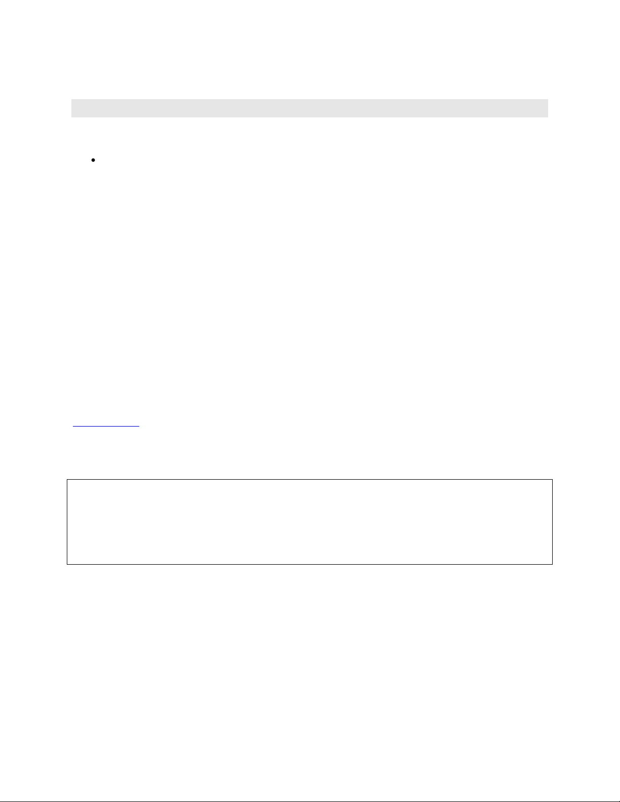
The base address of the CIO-DAS08-PGx is set by switching a bank of DIP
switches on the board (Figure 1-1). This bank of switches is labeled
ADDRESS and numbered 9 to 3.
Ignore the word ON and the numbers printed on the switch
The switch works by adding up the weights of individual switches to make a
base address. A 'weight' is active when the switch is down. Shown here,
switches 9 and 8 are down, all others are up. Weights 200H and 100H are
active, equaling 300H base address. The board is shipped with this default
address selected. If this address is already in use on your computer, select a
different address. Figure 1-1. Base address Select Switches
Table 1-1 lists the address ranges for the PC computer.
Table 1-1. Base Addresses
FUNCTIONHEX RANGEFUNCTIONHEX RANGE
EGA2C0-2CF8237 DMA #1000-00F
EGA2D0-2DF8259 PIC #1020-021
GPIB (AT)2E0-2E78253 TIMER040-043
SERIAL PORT2E8-2EF8255 PPI (XT)060-063
SERIAL PORT2F8-2FF8742 CONTROLLER (AT)060-064
PROTOTYPE CARD300-30FCMOS RAM & NMI MASK (AT)070-071
PROTOTYPE CARD310-31FDMA PAGE REGISTERS080-08F
HARD DISK (XT)320-32F8259 PIC #2 (AT)0A0-0A1
PARALLEL PRINTER378-37FNMI MASK (XT)0A0-0AF
SDLC380-38F8237 #2 (AT)0C0-0DF
SDLC3A0-3AF80287 NUMERIC CO-P (AT)0F0-0FF
MDA3B0-3BBHARD DISK (AT)1F0-1FF
PARALLEL PRINTER3BC-3BFGAME CONTROL200-20F
EGA3C0-3CFEXPANSION UNIT (XT)210-21F
CGA3D0-3DFBUS MOUSE238-23B
SERIAL PORT3E8-3EFALT BUS MOUSE23C-23F
FLOPPY DISK3F0-3F7PARALLEL PRINTER270-27F
SERIAL PORT3F8-3FFEGA2B0-2BF
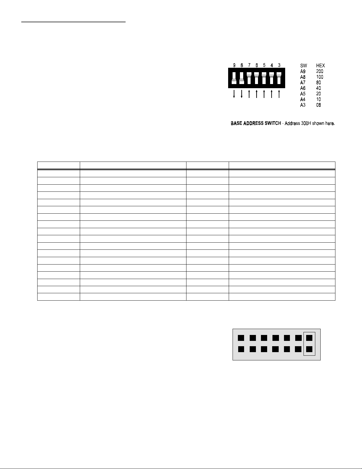
1.2.2 Interrupt Level Select
The interrupt jumper need only be set if the software you are using
requires it. If you do set the interrupt jumper, please check your PC's
current configuration for interrupt conflicts, and do not use IR2 in PC/AT
class machines (or higher).
There is a jumper block on the CIO-DAS08-PGx located just above the
PC bus interface (gold pins). The factory default setting is that no
interrupt level is set. The jumper is in the 'X' position (Figure 1-2).
If you need to pace conversions through hardware (either the on - board
pacer or an external clock), move this jumper to one of the other positions
(see table 1-2). Figure 1-2. Interrupt Select Jumper Block
2
INTERRUPT JUMPER BLOCK - Jumper in
X position = No IRQ.
234567X
Page 7
The following table shows some typical interrupt assignments on a PC. The CIO-DAS08-PGx use interrupt levels 2 through 7.
The levels most often available are 5 and 7.
Table 1-2. IRQ Assignments
DESCRIPTIONNAMEDESCRIPTIONNAME
REAL TIME CLOCK (AT)IRQ8PARITYNMI
RE-DIRECTED TO IRQ2IRQ9TIMERIRQ0 (AT)
UNASSIGNEDIRQ10KEYBOARDIRQ1
IRQ2
UNASSIGNEDIRQ11RESERVED (XT)
INT 8-15 (AT)
UNASSIGNEDIRQ12COM OR SDLCIRQ3
80287 NUMERIC CO-PIRQ13COM OR SDLCIRQ4
HARD DISKIRQ14HARD DISK (XT) or LPT (AT)IRQ5
UNASSIGNEDIRQ15FLOPPY DISKIRQ6
LPTIRQ7
NOTE: IRQ8-15 are AT only.
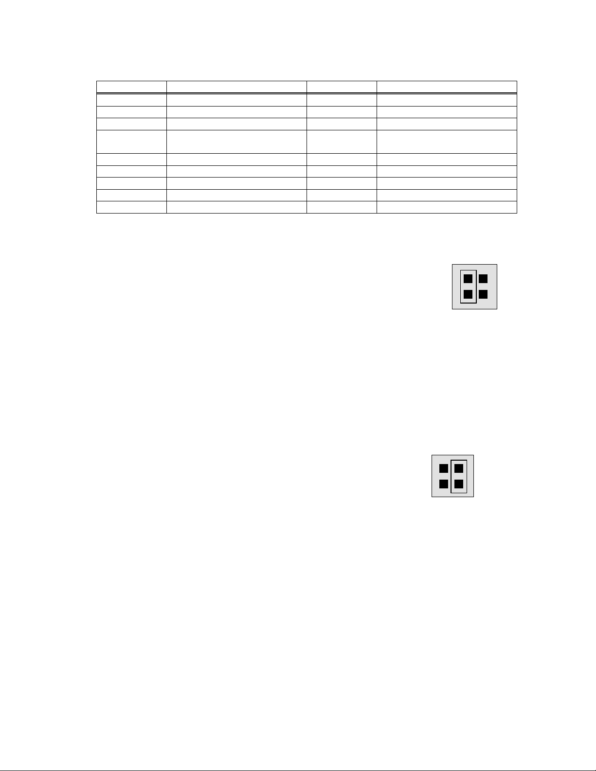
1.2.3 XTAL/PC Bus Clock Jumper
The A/D pacer clock sources for the MetraByte DAS-8PGA differs from the DAS-8.
The source for the DAS-8PGA is fixed at 1 MHz while the source for the DAS-8 gets
its clock pulse from the PC Bus Clock.
1 MHz
CLK
BUS
The CIO-DAS08-PGx pacer clock is selected by jumper to satisfy software written
for either board (Figure 1-3). The default choice for this jumper is the 1 MHz
position. You can alternately select the PC Bus Clock as the source for the A/D pacer
clock.
CLOCK SOURCE JUMPER - For a
standard DAS-8PGA 1 MHz A/D
Pacer Clock, place the jumper on the
two leftmost pins. For a DAS-8 type
A/D Pacer from PC Bus Clk, place the
jumper on the two rightmost pins.
Figure 1-3. Pacer Clock Select Jumper
1.2.4 Wait State
A wait state can be enabled on the CIO-DAS08-PGx by selecting WAIT STATE ON
at the jumper provided on the board. Enabling the wait state causes the personal
O
O
F
N
F
computer's bus transfer rate to slow down for board reads and writes ..
The wait state jumper is provided in case your computer ever has an I/O bus transfer
rate which is too fast for the CIO-DAS08-PGA. If your board were to fail sporadically
in random ways, try selecting the wait state ON.
WAIT STATE JUMPER BLOCK - A
wait state is not selected on this
jumper block. For a wait state,
place the jumper on the two
leftmost pins.
Figure 1-4. Wait State Jumper Block
1.2.5 Installing The CIO-DAS08-PGx In The Computer
1. Turn the power off.
2. Remove the cover of your computer. Please be careful not to dislodge any of the cables installed on the boards in your
computer as you slide the cover off.
3. Locate an empty expansion slot in your computer.
WAIT
STATE
4. Push the board firmly down into the expansion bus connector. If it is not seated fully it may fail to work and could short circuit
the PC bus power onto a PC bus signal. This could damage the motherboard in your PC as well as the board.
3
Page 8
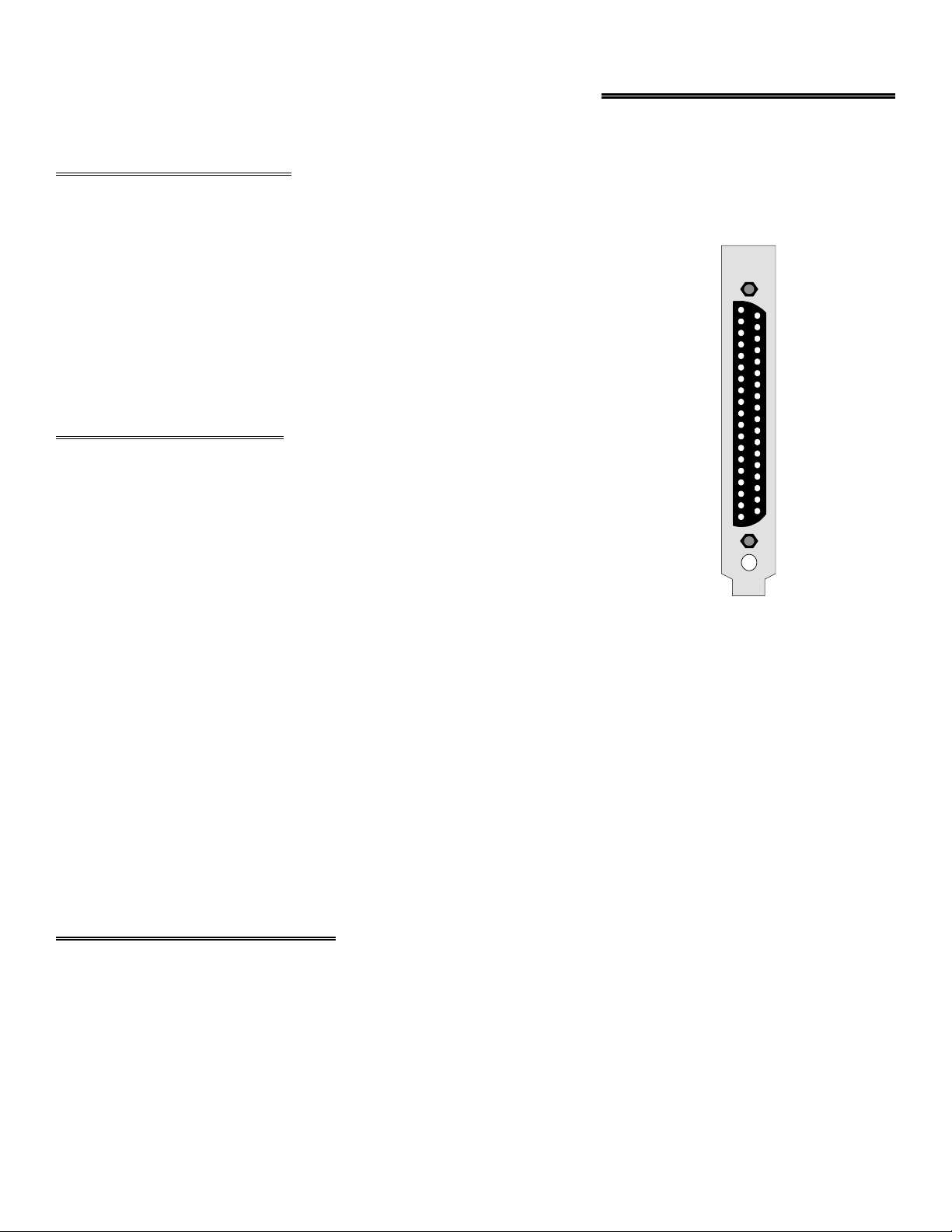
2.1 CONNECTOR DIAGRAM
The analog connector is a 37-pin, D-type connector accessible from the rear of
the PC through the expansion backplate (Figure 2-1).
2: SIGNAL CONNECTION
The connector accepts female 37 D-type connectors, such as those on the
C73FF-2, 2 foot cable with connectors.
If frequent changes to signal connections or signal conditioning is required,
please refer to the information on the CIO-TERMINAL and CIO-MINI37
screw terminal boards, CIO-EXP32, 32 channels analog MUX/AMP. Isolation
amplifiers can be mounted using the ISO-RACK08 and 5B isolation modules.
2.2 DIFFERENTIAL INPUTS
Differential inputs are 3-wire analog hookups consisting of a signal high, signal
low and chassis ground. The benefits of differential inputs are the ability to
CH0 LO 19
CH1 LO 18
CH2 LO 17
CH3 LO 16
CH4 LO 15
CH5 LO 14
CH6 LO 13
CH7 LO 12
LLGND 11
DIGITAL OUT 4 10
DIGITAL OUT 3 9
DIGITAL OUT 2 8
DIGITAL OUT 1 7
COUNTER 2 OUT 6
COUNTER 1 OUT 5
COUNTER 1 IN 4
COUNTER 0 OUT 3
COUNTER 0 IN 2
+15 FROM DC/DC 1
37 CH0 HIGH
36 CH1 HIGH
35 CH2 HIGH
34 CH3 HIGH
33 CH4 HIGH
32 CH5 HIGH
31 CH6 HIGH
30 CH7 HIGH
29 +5 VOLTS
28 DIG GND
27 DIGITAL IN 3
26 DIGITAL IN 2
25 DIGITAL IN 1
24 INTERRUPT INPUT
23 GATE 2
22 GATE 1
21 GATE 0
20 -15V FROM DC/DC
reject noise which affects both signal high and low, and the ability to
compensate for ground loops or potentials between signal low and chassis
ground.
Figure 2-1. Analog Connector
Although differential inputs are often preferable to single ended inputs, there are occasions when the floating nature of a
differential input can confound attempts to make a reading. In those cases, the inputs can be converted to modified differential.
Examine the diagram of the CIO-DAS08-PGx board. Near the 37-pin connector is located a position for an optional Single Inline
Package (SIP) of resistors. Installing the SIP converts the analog inputs from fully differential to modified differential with a
resistive reference to ground. A SIP resistor network is included with the board for this purpose.
NOTE:
When using the CIO-DAS08-PGx with the CIO-EXP16 or CIO-EXP32, the optional SIP resistor must be
installed. The CIO-EXP16 and CIO-EXP32 (and MetraByte EXP16) were designed to interface to a single-ended input.
Failure to install the SIP resistor when the board is used with these expansion boards will result in floating, unstable
readings.
Special instructions and solder are packaged with the SIP resistor. Follow the installation instructions carefully
and use the solder provided. Use of any other solder, or failure to follow instructions can result in a degradation
of the analog input's accuracy and may require out-of-warranty repair
.
2.3 DIGITAL OUTPUTS & INPUTS
All the digital outputs inputs on the CIO-DAS08-PGx are TTL level. TTL is an electronics industry term, short for Transistor
Transistor Logic, with describes a standard for digital signals which are either at 0V or 5V.
4
Page 9
3: ANALOG CONNECTIONS
3.1 ANALOG INPUTS
Prior to jumping into actual connection schemes, you should have at least a basic understanding of Single-Ended/Differential
inputs and system grounding/isolation. If you are already comfortable with these concepts you may wish to skip to the next section
(on wiring configurations).
3.1.1 Single-Ended and Differential Inputs
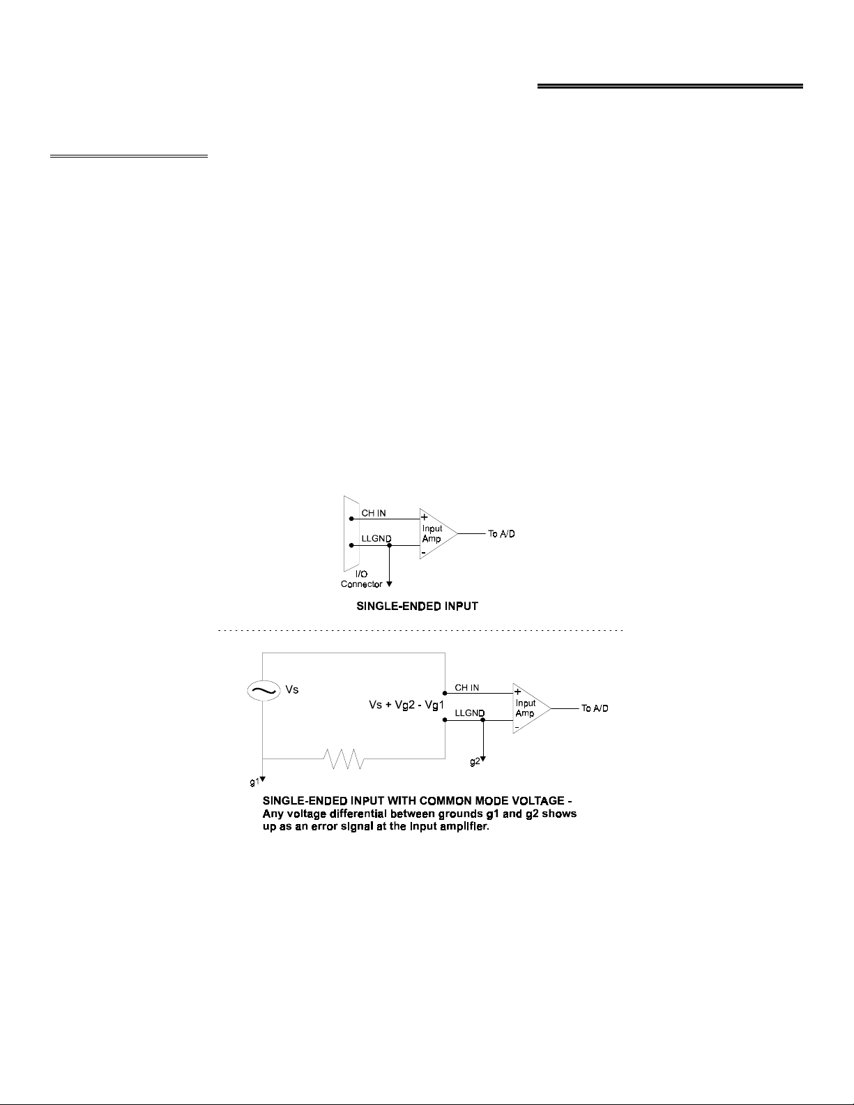
The CIO-DAS08-PGx provides either 8 differential or 16 single-ended input channels. The concepts of single-ended and
differential inputs are discussed in the following section
Single-Ended Inputs
A single-ended input measures the voltage between the input signal and ground. In this case, in single-ended mode the
CIO-DAS08-PGx measures the voltage between the input channel and LLGND. The single-ended input configuration requires
only one physical connection (wire) per channel and allows the board to monitor more channels than the differential configuration
using the same connector and onboard multiplexer (Figure 3-1). However, since the CIO-DAS08-PGx is measuring the input
voltage relative to its own low level ground, single-ended inputs are more susceptible to both EMI (electro magnetic interference)
and any ground noise at the signal source. The following diagrams show the single-ended input configuration. Note: For
simplicity, the input multiplexer is not shown.
.
Figure 3-1. Single-Ended Input Configuration (Simplified)
5
Page 10

3.1.2 Differential Inputs
Differential inputs measure the voltage between two distinct input signals. Within a certain range (referred to as the common mode
range), the measurement is almost independent of signal source to CIO-DAS08-PGA ground variations. A differential input is also
much more immune to EMI than a single-ended one. Most EMI noise induced in one lead is also induced in the other, the input
only measures the difference between the two leads, and the EMI common to both is ignored. This effect is a major reason there is
twisted pair wire as the twisting assures that both wires are subject to virtually identical external influence. Figure 3-2 below
shows a typical differential input configuration.
Figure 3-2. Differential Input Configuration
6
Page 11

Before moving on to the discussion of grounding and isolation, it is important to explain the concepts of common mode, and
common mode range (CM Range). Common mode voltage is depicted in Figure 3-2 as Vcm. Though differential inputs measure
the voltage between two signals, without (almost) respect to the either signal’s voltages relative to ground, there is a limit to how
far away from ground either signal can go. Though the CIO-DAS08-PGx has differential inputs, it will not measure the difference
between 100V and 101V as 1 Volt (in fact the 100V would destroy the board!). This limitation or common mode range is depicted
graphically in Figure 3-3. The CIO-DAS08-PGx common mode range is +/- 10 Volts. Even in differential mode, no input signal
can be measured if it is more than 10V from the board’s low level ground (LLGND).
+13V
+12V
+11V
+10V
+9V
+8V
+7V
+6V
+5V
+4V
+3V
+2V
+1V
-1V
-2V
-3V
-4V
-5V
-6V
-7V
-8V
-9V
-10V
-11V
-12V
-13V
3.1.3 System Grounds and Isolation
Gray area represents common mode range
Both V+ and V- must always re ma in w ithin
the common m ode range re la tiv e to L L Gn d
With Vcm= +5VDC,
+Vs must be less than +5V, or the comm on m ode range w ill be e x c eeded (>+10V)
Vcm
Vcm (Common M ode Voltage) = +5 Volts
Figure 3-3. Common Mode Range Limits
There are three scenarios possible when connecting your signal source to your board.
1. The board and the signal source may have the same (or common) ground. This signal source can be connected directly to the
board.
2. The board and the signal source may have an offset voltage between their grounds (AC and/or DC). This offset it commonly
referred to a common mode voltage. Depending on the magnitude of this voltage, it may or may not be possible to connect
the board directly to your signal source. We will discuss this topic further in a later section.
3. The board and the signal source may already have isolated grounds. This signal source may be connected directly to the
board.
3.1.4 Which system do you have?
Try the following experiment. Using a battery powered voltmeter
1
, measure the voltage (difference) between the ground signal at
your signal source and at your PC. Place one voltmeter probe on the PC ground and the other on the signal source ground.
Measure both the AC and DC Voltages.
If both AC and DC readings are 0.00 volts, you may have a system with common grounds. However, since voltmeters will average
out high frequency signals, there is no guarantee. Please refer to the section below titled Common Grounds.
1
If you do not have access to a voltmeter, skip the experiment and take a look at the following three sections. You may be able to identify your system type from the
descriptions provided.
7
Page 12

If you measure reasonably stable AC and DC voltages, your system has an offset voltage between the grounds category. This
offset is referred to as a Common Mode Voltage. Please be careful to read the following warning and then proceed to the section
describing Common Mode systems.
WARNING
If either the AC or DC voltage is greater than 10 volts, do not connect the CIO-DAS08-PGA to this signal
source. You are beyond the boards usable common mode range and will need to either adjust your grounding
system or add special Isolation signal conditioning to take useful measurements. A ground offset voltage of
more than 30 volts will likely damage the board and possibly your computer. Note that an offset voltage much
greater than 30 volts will not only damage your electronics, but it can also be hazardous to your health.
If you cannot obtain a reasonably stable DC voltage measurement between the grounds, or the voltage drifts around considerably,
the two grounds are most likely isolated. The easiest way to check for isolation is to change your voltmeter to it’s ohm scale and
measure the resistance between the two grounds. It is recommended that you turn both systems off prior to taking this resistance
measurement. If the measured resistance is more than 100 Kohm, it’s a fairly safe bet that your system has electrically isolated
grounds.
3.1.5 Systems with Common Grounds
In the simplest (but perhaps least likely) case, your signal source will have the same ground as the CIO-DAS08-PGx. This would
typically occur when providing power or excitation to your signal source directly from the board. There may be other common
ground configurations, but it is important to note that any voltage between the board ground and your signal source ground is a
potential error voltage if you set up your system based on a common ground assumption.
As a safe rule of thumb, if your signal source or sensor is not connected directly to an LLGND pin on your board, it’s best to
assume that you do not have a common ground even if your voltmeter measured 0.0 Volts. Configure your system as if there is
ground offset voltage between the source and the board. This is especially true if you are using the board at high gains, since
ground potentials in the sub millivolt range will be large enough to cause A/D errors, yet will not likely be measured by your
handheld voltmeter.
3.1.6 Systems with Common Mode (ground offset) Voltages
The most frequently encountered grounding scenario involves grounds that are somehow connected, but have AC and/or DC offset
voltages between the board and signal source grounds. This offset voltage my be AC, DC or both and may be caused by a wide
array of phenomena including EMI pickup, resistive voltage drops in ground wiring and connections, etc. Ground offset voltage is
a more appropriate term to describe this type of system, but since our goal is to keep things simple, and help you make appropriate
connections, we’ll stick with our somewhat loose usage of the phrase Common Mode.
3.1.7 Small Common Mode Voltages
If the voltage between the signal source ground and board ground is small, the combination of the ground voltage and input signal
will not exceed the CIO-DAS800’s +/-10V common mode range, (i.e. the voltage between grounds, added to the maximum input
voltage, stays within +/-10V), This input is compatible with the CIO-DAS08-PGx and the system can be connected without
additional signal conditioning. Fortunately, most systems will fall in this category and have a small voltage differential between
grounds.
3.1.8 Large Common Mode Voltages
If the ground differential is large enough, the +/- 10V common mode range will be exceeded (i.e. the voltage between the board
and signal source grounds, added to the maximum input voltage you’re trying to measure exceeds +/-10V). In this case the board
cannot be directly connected to the signal source. You will need to change your system grounding configuration or add isolation
signal conditioning. (Please look at our ISO-RACK and ISO-5B-series products to add electrical isolation, or give our technical
support group a call to discuss other options).
WARNING
Relying on the earth prong of a 120VAC for signal ground connections is not advised.. Different ground plugs
may have large and potentially even dangerous voltage differentials. Remember that the ground pins on
120VAC outlets on different sides of the room may only be connected in the basement. This leaves the
possibility that the “ground” pins may have a significant voltage differential (especially if the two 120 VAC
outlets happen to be on different phases!)
8
Page 13

3.1.9 Board and Signal Source Have Isolated Grounds
g
g
Some signal sources will already be electrically isolated from the board. Figure 3-4 shows a typical isolated ground system. These
signal sources are often battery powered, or are fairly expensive pieces of equipment (since isolation can be expensive), isolated
ground systems provide excellent performance, but require some extra effort during connections to assure optimum performance
is obtained. Please refer to the following sections for further details.
3.2 WIRING CONFIGURATIONS
Combining all the grounding and input type possibilities pro vides us with the following potential connection configurations. The
combinations along with our recommendations on usage are shown in Table 3-1 below.
Table 3-1. Analog Input Configuration Recommendations
GROUND
CATEGORY
INPUT
CONFIGURATION
OUR VIEW
RecommendedSingle-Ended InputsCommon Ground
AcceptableDifferential InputsCommon Ground
Common Mode
Voltage < +/-10V
Common Mode
Voltage < +/-10V
Common Mode
Voltage > +/- 10V
Common Mode
Voltage > +/-10V
Single-Ended Inputs
Differential Inputs
Not RecommendedSingle-Ended Inputs
RecommendedDifferential Inputs
Unacceptable without
adding Isolation
Unacceptable without
adding Isolation
AcceptableSingle-ended InputsAlready Isolated Grounds
Already Isolated
Grounds
RecommendedDifferential Inputs
The following sections depicts recommended input wiring schemes for each of the seven possible input configuration/grounding
combinations.
3.2.1 Common Ground / Single-Ended Inputs
Single-ended is the recommended co nfiguration for common ground co nnections. However, if some of your inputs are common
ground and some are not, we recommend you use the differential mode. There is no performance penalty (other than loss of
channels) for using a d ifferential input to measure a common ground signal source. H owever the reverse is not true . Figure 3-4
below shows a recommended connection diagram for a common ground / single-ended input system.
Signal
S our c e w ith
C om m o n G nd
Optional wire
since signal source
and A/D board share
common ground
Signal source and A/D board
sharin
common ground connected
to s in
le- en d e d in p u t.
I/O
Connector
CH IN
LL GND
+
Inp u t
Amp
-
A/D Board
To A / D
Figure 3-4. Common Ground / Single-Ended Inputs
9
Page 14

3.2.2 Common Ground / Differential Inputs
g
g
g
The use of differential inputs to monitor a signal source with a common ground is a acceptable configuration though it requires
more wiring and offers fewer channels than selecting a single-ended configuration. Figure 3-5 below shows the recommended
connections in this configuration.
Signal
So ur ce w ith
Co mm o n Gnd
Optional wire
since signal source
and A/D board sha re
common ground
Required conn ection
of LL GND to CH Low
I/O
Connector
CH High
CH Low
LL GND
+
Input
Amp
-
A/D Board
To A /D
Signal source and A/D board
sharin
com m on ground connected
to differential input.
Figure 3-5. Common Ground / Differential Inputs
3.2.3 Common Mode Voltage < +/-10V/Single-Ended Inputs
This is not a recommended configuration. In fact, the phrase common mode has no meaning in a single-ended system and this case
would be better d escribed as a system with offset grounds. Ho wever, you can try this configuration. No system damage should
occur and depending on the overall accuracy you require, you may receive acceptable results.
3.2.4 Common Mode Voltage < +/-10V/Differential Inputs
Systems with varying ground potentials should always be monitored in the differential mode. Care is required to assure that the
sum of the input signal and the ground differential (referred to as the common mode voltage) does not exceed the common mode
range of the A/D board (+/-10V on the CIO-DAS08-PGx). The diagram below show recommended connections in this
configuration.
Signal Source
w ith Com mon
Mo d e V o lta g e
The voltage differential
between these grounds,
added to the maximum
input signal must stay
within +/-10 V
GND
I/O
Connector
CH Hi
CH Low
LL GND
h
+
Inp ut
Amp
-
A/D Board
To A / D
Signal source and A/D board
with common m ode volta
e
connected to a differential input.
Figure 3-6. Common Mode Voltage < +/-10V/Differential Inputs
10
Page 15

3.2.5 Common Mode Voltage > +/-10V
g
g
g
g
g
g
g
g
g
g
g
g
g
g
The CIO-DAS08-PGx will not directly monitor signals with common mode voltages greater than +/-10V. You will either need to
alter the system ground configuration to reduce the overall common mode voltage, or add isolated signal conditioning between the
source and your board. See Figures 3-7 and 3-8.
Iso la tio n
Barrier
arge common
L
mode voltage
between signal
source & A/D board
When the voltage difference
between si
A/D board
enou
common mode ran
exceeded, isolated si
conditionin
GND
nal source and
round is large
h so the A/D board’s
must be added.
e is
CH IN
I/O
Conn ector
LL GND
+
-
Input
Amp
To A /D
A/D Board
nal
System with a Large Common Mode Voltage,
Connected to a Sin
le-Ended Input
Figure 3-7. Common Mode Voltage - >+/- 10V Single-Ended Input
Isolation
Barrier
arge comm on
L
mode voltage
between signa l
source & A /D b o a rd
When the voltage difference
between si
A/D board
enou
comm on m ode ran
exceeded, isolated si
conditionin
GND
nal source and
round is large
h so the A/D board’s
must be added.
CH Hi
h
+
Inpu t
Amp
-
A/D Board
I/O
Connector
CH Low
LL GND
10 K
e is
nal
10K is a recommended value. You may short LL GND to CH Low
instead, but this will reduce your system’s noise immunity.
To A / D
System with a Large Comm on Mode Voltage,
Connected to a Differential Input
Figure 3-8. Common Mode Voltage - >+/- 10V Differential Input
11
Page 16

3.2.6 Isolated Grounds / Single-Ended Inputs
g
Single-ended inputs can be used to monitor isolated inputs, though the use of the differential mode will increase you system’s
noise immunity. Figure 3-9 below shows the recommended connections is this configuration.
Isolated
signal
s o urc e
CH IN
LL GND
I/O
Connector
+
Inpu t
Amp
To A /D
-
A/D Board
Isolated Signal Source
Connected to a Single-Ended Input
Figure 3-9 . Isolated Grounds - Single-Ended Inputs
3.2.7 Isolated Grounds / Differential Inputs
Optimum performance with isolated signal sources is assured with the use of the differential input setting. Figure 3-10 shows the
recommend connections is this configuration..
Signal Source
an d A/D Bo a rd
A lread y I s o la ted .
GND
10 K
CH High
CH Low
LL GND
+
-
Input
Amp
To A /D
These
rounds are
electrically isolated.
I/O
Connector
10K is a recomm ended value. You may short LL GN D to CH Low
instead, b ut this will reduce your system’s noise imm unity.
A/D Board
Already isolated signal source
and A/D board connected to
a differential input.
Figure 3-10. Isolated Grounds - Differential Inputs
12
Page 17

4: REGISTER ARCHITECTURE
4.1 CONTROL & DATA REGISTERS
The CIO-DAS08-PGx is controlled and monitored by writing to and reading from eight consecutive 8-bit I/O addresses. The first
address, or BASE ADDRESS, is determined by setting a bank of switches on the board.
Register manipulation is best left to experienced programmerss as most of the possible functions are implemented in easy to use
Universal Library™.
The register descriptions follow the format:
Where the numbers along the top row are the bit positions within the 8-bit byte and the numbers and symbols in the bottom row is
the function associated with each bit.
To write to or read from a register in decimal or HEX, the bit weights listed in table 4-1 apply.
01234567
A/D8A/D7A/D6A/D5A/D4A/D3A/D2A/D1
Table 4-1. Register Bit Weights
HEX VALUEDECIMAL VALUEBIT POSITION
110
221
442
883
10164
20325
40646
801287
To write control words or data to a register, the individual bits must be set to 0 or 1 then combined to form a byte.
The method of programming required to read/write bits from bytes is beyond the scope of this manual.
In summary form, the registers and their function are listed in Table 4-2. Each register has eight bits which may constitute a byte
of data or eight individual bit read/write functions.
Table 4-2. Board Register Functions
WRITE FUNCTIONREAD FUNCTIONADDRESS
Start 8 Bit A/D ConversionA/D Bits 9-12 (LSB)BASE
Start 12 Bit A/D ConversionA/D Bits 1(MSB)-8BASE +1
BASE +2
EOC, IP1-IP3, IRQ, MUX
Address
OP1-OP4, INTE & MUX
Address
Programmable Gain ControlChannel MUX and Gain StatusBASE +3
Load Counter 0Read Counter 0BASE +4
Load Counter 1Read Counter 1BASE +5
Load Counter 2Read Counter 2BASE +6
Counter ControlNot UsedBASE +7
13
Page 18

4.2 A/D DATA REGISTER
BASE ADDRESS (Read / Write)
READ
On read, it contains the least significant four digits of the analog input data.
These four bits of analog input data must be combined with the eight bits of analog input data in BASE + 1, forming a complete
12 bit number. The data is in the format 0 = minus full scale. 4095 = +FS.
WRITE
Writing any data to the register causes an immediate 8-bit A/D conversion.
BASE + 1 (Read / Write)
READ
On read, the most significant A/D byte is read.
01234567
0000A/D12 LSBA/D11A/D10A/D9
01234567
A/D8A/D7A/D6A/D5A/D4A/D3A/D2A/D1 MSB
The A/D Bits code corresponds to the voltage on the input according to the table below.
UNIPOLARBIPOLARHEXDECIMAL
+Full Scale+Full ScaleFFF4095
½ Full Scale0 Volts8002048
00
WRITE
Writing to this register starts a 12-bit A/D conversion.
A note of caution: Place several NO-OP instructions between consecutive 12-bit A/D conversions to avoid over-running the A/D
converter.
−
Full Scale
0 Volts
4.3 STATUS AND CONTROL REGISTER
BASE + 2 (Read / Write) Read Functions
READ = STATUS
EOC = 1 the A/D is busy converting and data should not be read.
01234567
MUX0MUX1MUX2IRQIP1IP2IP3EOC
EOC = 0 the A/D is not busy and data can be read.
IP3 to IP1 are the digital input lines on the 37 pin analog connector.
IRQ is the status of an edge triggered latch connected to Interrupt Input (pin 24) of the analog connector. It is high (1) when a
positive edge has been detected. It can be reset to 0 by writing to the INTE mask at BASE + 2 write.
14
Page 19

MUX 2 to MUX 0 is the current multiplexer channel. The current channel is a binary coded number between 0 and 7 .
WRITE = CONTROL
BASE + 2 (Read / Write) Write Functions
OP4 to OP1 are the digital output lines on the 37 pin analog connector.
INTE = 1 enables interrupts (positive edge triggered) onto the PC bus IRQ selected via the IRQ jumper on the CIO-DAS08-PGA.
INTE = 0 disables the passing of the interrupt detected at pin 24 to the PC bus.
IRQ is set to 1 every time an interrupt occurs. If you want to process successive interrupts then set INTE = 1 as the last step in
your interrupt service routine.
MUX2 to MUX0. Set the current channel address by writing a binary coded number between 0 and 7 to these three bits.
NOTE
Every write to this register sets the current A/D channel MUX setting to the number in bits 2-0.
4.4 PROGRAMMABLE GAIN REGISTER
01234567
MUX0MUX1MUX2INTEOP1OP2OP3OP4
The register's layout when written to is :
BASE + 3 (Read / Write) Write Functions
The register's layout when read from is :
BASE + 3 (Read / Write) Read Functions
The gain/range of a board is controlled by writing a control code to the register. The codes are as follows:
CONTROL CODESBI-POLAR
CIO-DAS08-PGH
10.00.5
5.01
1.05
0.510
0.150
0.05100
0.01500
0.0051000
BIT 0BIT 1BIT 2BIT 3BIT 4BIT 5BIT 6BIT 7
R0R1R2R3XXXX
BIT 0 BIT 1BIT 2BIT 3BIT 4BIT 5BIT 6BIT 7
R0R1R2R3MA0MA1MA2X
R0R1R2R3HEXDECRANGE VGAIN
000188+
000000+
0101A10+
010022+
0011C12+
001044+
0111E14+
011066+
CIO-DAS08-PGH
CONTROL CODESUNI-POLAR
R0R1R2R3HEXDECRANGE VGAIN
1000110 to 10.01
1100330 to 1.010
1010550 to 0.1100
1110770 to 0.011,000
15
Page 20

There are fewer ranges available for the CIO-DAS08-PGL. Gains of 2, 4 & 8 are often called binary gains. These ranges are not
available on the MetraByte DAS-8PGA.
CONTROL CODESBI-POLAR
CIO-DAS08-PGL
R0R1R2R3HEXDECRANGE VGAIN
10.00.5
5.01
2.52
1.254
0.6258
CONTROL CODESUNI-POLAR
CIO-DAS08-PGL
CONTROL CODESBI-POLAR
CIO-DAS08-PGM
10.00.5
5.01
0.52
0.054
000188+
000000+
010022+
004044+
011066+
R0R1R2R3HEXDECRANGE VGAIN
1000110 to10.01
1100330 to 5.02
1010550 to 2.54
1100770 to 1.258
R0R1R2R3HEXDECRANGE VGAIN
000188+
000000+
0101A10+
0011C12+
0111E14+0.018
CONTROL CODESUNI-POLAR
CIO-DAS08-PGM
R0R1R2R3HEXDECRANGE VGAIN
1001990 to10.01
1101B110 to 1.02
1010D130 to 0.14
1111F150 to 0.018
To set the input range of the CIO-DAS08-PGx board, select the desired range from the table and write the code in decimal or
hexadecimal to base address + 3. Here is an example in BASIC:
100 OUT &H303, 8 'Set gain = 0.5 (±10V range)
The range of the analog inputs is now set to ±10V or 2.44mV per bit (10/4096).
MA2 to MA0 = Indicates the analog input channel that is currently selected (by writing to base +2).
16
Page 21

4.5 COUNTER LOAD & READ REGISTERS
COUNTER 0
BASE ADDRESS + 4 (Read / Write)
COUNTER 1
BASE ADDRESS + 5 (Read / Write)
COUNTER 2
BASE ADDRESS + 6 (Read / Write)
The data in the counter read register, and the action taken on the data in a counter load register, is wholly dependent upon the
control code written to the control register.
The counters are 16-bit counters, each with an 8-bit window, the read / load register. Data is shifted into and out of the 16-bit
counters through these 8-bit windows according to the control byte.
You will need an 8254 data sheet if you want to program the 8254 directly at the register level.
01234567
D0D1D2D3D4D5D6D7
01234567
D0D1D2D3D4D5D6D7
01234567
D0D1D2D3D4D5D6D7
4.6 COUNTER CONTROL REGISTER
BASE ADDRESS + 7 (Write Only)
WRITE
SC1 to SC0 are the counter select bits. They are binary coded between 0 and 2.
RL1 to RL0 are the read and load control bits:
Latch Counter00
Read/load high byte10
Read/load low byte01
Read/load low the high byte (word transfer)11
M2 to M0 are the counter control operation type bits:
Change on terminal count000
Programmable one-shot100
Rate generator010
Square wave generator110
Software triggered strobe001
Hardware triggered strobe101
01234567
BCDM0M1M2RL0RL1SC0SC1
OPERATIONRL0RL1
OPERATION TYPEM0M1M2
BCD = 0 then counter data is 16-bit binary. (65,535 max)
17
Page 22

BCD = 1 then counter data is 4-decade Binary Coded Decimal. (9,999 max)
4.7 COUNTER/TIMER
The 82C54 counter/timer chip (Figure 4-1) may be used for event counting, frequency and pulse measurement and as a pacer
clock for the A/D converter. All the inputs, outputs and gates of the counter are accessible through the 37 pin analog connector
with the exception of the counter 2 input.
The counter is easy to understand. The GATE line determines whether or not TTL level pulses present at the CLK input will
decrement the counter. The OUT line then transitions (pulses or shifts) depending on the codes in the control register and the
count value in the count register.
The counter gates, inputs and outputs are all simple TTL.
The primary purpose of the counter timer chip is to pace the A/D samples. The input of counter 2 is jumper selectable for a
crystal controlled source or the PC bus clock source.
The PCLK signal is divided by 2 prior to the input at counter 2, therefore, if the PCLK signal on your PC/AT were 8 MHz, the
signal at the input of counter 2 would be 4MHz. The 10 MHz crystal source is divided by 10.
Assuming a 4 MHz signal at counter 2, the rates out of counter 2 (pin 6) can vary between 2 MHz (4 MHz / 2) to 61 Hz (4 MHz /
65,535). For rates slower than 61 Hz, wire the output of counter 2 to the input of counter 1. Next, wire the output of counter 1 to
the interrupt input (pin 24). The slowest rate is then once every 17 minutes.
When using the crystal source, the minimum rate would be about 15 Hz using only one counter.
10K
+5
RN1
10
10 MHz
CRYSTAL
1 MHz
2
21
2
22
4
23
CLK BUS
U8
3
GATE 0
CLK 0
GATE 1
CLK 1
GATE 2
CLK 2
COUNTER 0
COUNTER 1
COUNTER 2
U14
3
5
6
37 PIN
CON
PC BUS PCLK - B20
Figure 4-1. Counter /Timer Block Diagram
18
Page 23

4.8 DIGITAL INPUT
The digital inputs are simple TTL level lines. They feed into an 8-bit register which has other on-board signals fed into it. The
resultant 8-bit status byte can be read at BASE address + 2.
The digital inputs IP1, IP2 & IP3 can be used as status lines to trigger or hold off A/D conversions. Be aware of possible conflicts
when pacing conversions from the on - board pacer and simultaneously using IP1 through IP3 as general purpose digital inputs.
4.9 DIGITAL OUTPUT
The digital output lines, OP1, OP2, OP3 & OP4 are TTL level lines which are controlled with part of an 8-bit register located at
BASE address + 2.
The lines are used to control the multiplexer address on an external CIO-EXP32 differential amplifier/ multiplexer if one is
installed. For that reason, we recommend not using them as general purpose digital outputs.
19
Page 24

4.10 TRIGGER & INTERRUPT LOGIC
The trigger logic on the CIO-DAS08-PGx is quite simple. Pin 24 of the 37 pin connector is an input to a flip-flop which can be
read at BASE address + 2 on the IRQ bit. The board can be triggered by polling this bit until a trigger pulse (rising edge) has
occurred. It must be reset by a write to BASE + 2 before it will respond to additional rising edges.
By writing a 1 to the INTE control bit at BASE + 2, the rising edge detected by the flip-flop will be translated into an interrupt
pulse which can be used to interrupt the CPU's 8259 interrupt controller on the PC motherboard.
The interrupt level jumper on the board may need to be installed. Move it from the 'X' (default) position to the IRQ number you
want the interrupt pulse on.
The 82C54 counter/timer chip is primarily a pacer for A/D samples. It is an integral part of the trigger logic. To employ the 82C54
as an A/D pacer, wire the output of the counter (pin 6) that you will program to provide pacing pulses directly into the Interrupt
Input (pin 24).
20
Page 25

5: SPECIFICATIONS
Power consumption
+5V: 900 mA typical, 1125 mA max
Analog input section
A/D converter type AD574
Resolution 12 bits
Number of channels 8 differential (configurable as quasi-differential via installation of SIP resistor)
Input Ranges
CIO-DAS08/PGH ±10V, ±5V, ±1V, ±0.5V , ±0.1V, ±0.05V, ±0.01V, ±0.005V, 0 to 10V, 0 to 1V, 0 to
0.1V, 0 to 0.01V software selectable
CIO-DAS08/PGL ±10V, ±5V, ±2.5V, ±1.25V, ±0.625V, 0 to 10V, 0 to 5V, 0 to 2.5V, 0 to 1.25V
software selectable
CIO-DAS08/PGM ±10V, ±5V, ±0.5V, ±0.05V, ±0.01V, 0 to 10V, 0 to 1V, 0 to 0.1V, 0 to 0.01V
software selectable
Polarity Unipolar/Bipolar, software selectable
A/D pacing Internal counter or external source (Interrupt Input, jumper selectable, rising edge) or
software polled
A/D Trigger sources External hardware/software (Digital In 1)
Data transfer Interrupt or software polled
DMA None
A/D conversion time 25 µs
Throughput 20 kHz, PC dependent
Accuracy ±0.01% of reading ±1 LSB
±0.05% of full scale
Differential Linearity error ±1 LSB
Integral Linearity error ±0.5 LSB
No missing codes guaranteed 12 bits
Gain drift (A/D specs) ±25 ppm/°C
Zero drift (A/D specs) ±10µV/°C
Common Mode Range ±10V
CMRR 72 dB
Input leakage current (@25 Deg C) 100 nA
Input impedance 10 Meg Ohms min
Absolute maximum input voltage ±35
Digital Input / Output
Digital Type (main connector)
Output: 74LS273
Input: 74LS244
Configuration 4 fixed output bits, 3 fixed input bits
Number of channels 4 out, 3 in
Output High 2.7 volts min @ −0.4mA
Output Low 0.4 volts max @ 8 mA
Input High 2.0 volts min, 7 volts absolute max
Input Low 0.8 volts max, −0.5 volts absolute min
Interrupts 2 - 7, jumper selectable
Interrupt enable Programmable
Interrupt sources External (Interrupt In), rising edge
21
Page 26

Counter section
Counter type 82C54
Configuration 3 down-counters, 16 bits each
Counter 0 - independent, user configurable
Source: user connector (Counter 0 In)
Gate: user connector (Gate 0)
Output: user connector (Counter 0 Out)
Counter 1 - independent, user configurable
Source: user connector (Counter 1 In)
Gate: user connector (Gate 1)
Output: user connector (Counter 1 Out)
Counter 2 - independent, user configurable
Source: 1 MHz (from 10MHz Xtal via divide-by-ten) or PC SysClk (via divide by 2 circuit)
selectable by jumper
Gate: user connector (Gate 2)
Output: user connector (Counter 2 Out)
Clock input frequency 10 Mhz max
High pulse width (clock input) 30 ns min
Low pulse width (clock input) 50 ns min
Gate width high 50 ns min
Gate width low 50 ns min
Input low voltage 0.8V max
Input high voltage 2.0V min
Output low voltage 0.4V max
Output high voltage 3.0V min
Environmental
Operating temperature range 0 to 50°C
Storage temperature range −20 to 70°C
Humidity 0 to 95% non-condensing
22
Page 27

EC Declaration of Conformity
We, Measurement Computing Corp., declare under sole responsibility that the product:
CIO-DAS08-PGx
DescriptionPart Number
to which this declaration relates, meets the essential requirements, is in conformity with, and CE marking has been applied according to
the relevant EC Directives listed below using the relevant section of the following EC standards and other normative documents:
EU EMC Directive 89/336/EEC: Essential requirements relating to electromagnetic compatibility.
EU 55022 Class B: Limits and methods of measurements of radio interference characteristics of information technology equipment.
EN 50082-1: EC generic immunity requirements.
IEC 801-2: Electrostatic discharge requirements for industrial process measurement and control equipment.
IEC 801-3: Radiated electromagnetic field requirements for industrial process measurements and control equipment.
IEC 801-4: Electrically fast transients for industrial process measurement and control equipment.
Carl Haapaoja, Director of Quality Assurance
Page 28

Measurement Computing Corporation
10 Commerce Way
Suite 1008
Norton, Massachusetts 02766
(508) 946-5100
Fax: (508) 946-9500
E-mail: info@mccdaq.com
www.mccdaq.com
 Loading...